

®
LOW DROP POWER SCHOTTKY RECTIFIER
MAIN PRODUCT CHARACTERISTIC S
STPS3L25S
I
F(AV)
V
RRM
3 A
25 V
Tj (max) 150° C
(max) 0.44 V
V
F
FEATURES AND BENEFITS
VERY LOW F O RW ARD VOLTAG E DROP FOR
LESS POWER DISSIPATION
OPTIMIZED CONDUCTION/REVERSE LOSSES
TRADE-OFF WHICH MEANS THE HIGHEST
EFFICIENCY IN THE APPLICATIONS
HIGH POWER SURFACE MOUNT MINIATURE
PACKAGE
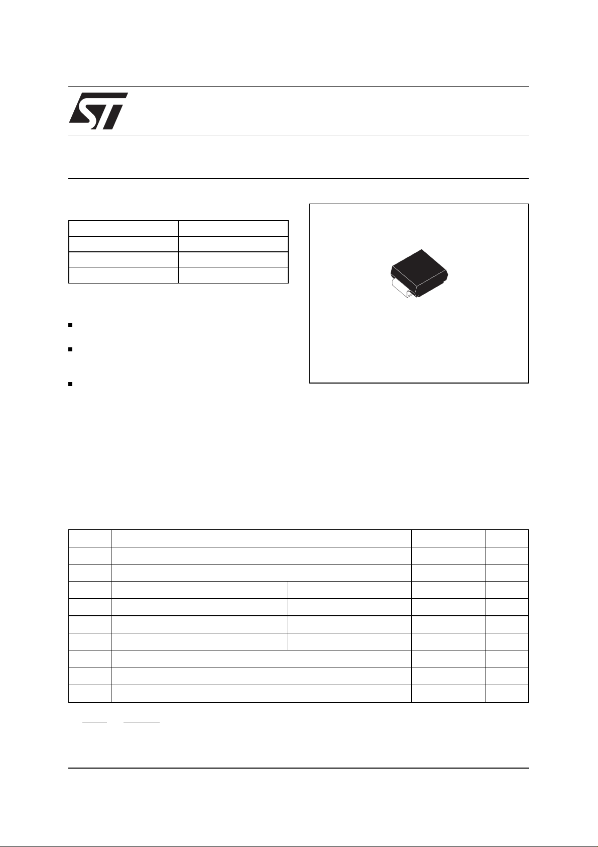
DESCR IPTION
Single Schottky rectifier suited t o Switched Mode
Power Supplies and high frequency DC to DC converters.
Packaged in SMC, this device is especially intended for use as an antiparallel diode on synchronous rectification freewheel MOSFET’s at the
secondary of 3.3V SMP S and DC/ DC units.
ABSOLUTE RATINGS
(limiting values)
SMC
JEDEC DO-214AB
Symbol Parameter Value Unit
V
RRM
I
F(RMS)
I
F(AV)
I
FSM
I
RRM
I
RSM
T
stg
Tj Maximum operating junction temperature * 150
Repetitive peak reverse voltage 25 V
RMS forward current 10 A
Average forward current TL = 115°C
δ
= 0.5 3 A
Surge non repetitive forward current tp = 10 ms Sinusoidal 75 A
Repetitive peak reverse current tp= 2 µs square F=1kHz 1 A
Non repetitive peak reverse current tp = 100 µs square 1 A
Storage temperature range - 65 to + 150
°
°
dV/dt Critical rate of rise of reverse voltage 10000 V/µs
dPtot
* :
June 1999 - Ed: 3A
dTj
<
1
Rth(j−a
thermal runaway condition for a diode on its own heatsink
)
C
C
1/4
STPS3L25S
THERMAL RESISTANCES
Symbol Parameter Value Un it
R
th(j-l)
Junction to lead 20
STATIC ELECTRICAL CHARACTE RISTICS
Symbol Tests Conditions Tests Conditions Min. Typ. Max. Unit
* Reverse leakage current Tj = 25°CV
I
R
= V
R
RRM
90
Tj = 125°C1530mA
* Forward voltage drop Tj = 25°CI
V
F
= 3 A 0.49 V
F
Tj = 125°C0.370.44
Tj = 25°CI
= 6 A 0.6
F
Tj = 125°C 0.5 0.58
Pulse test : * tp = 380 µs, δ < 2%
To evaluate the maximum conduction losses use the following equation :
P = 0.3 x I
+ 0.047 I
F(AV)
F2(RMS)
°
C/W
µ
A
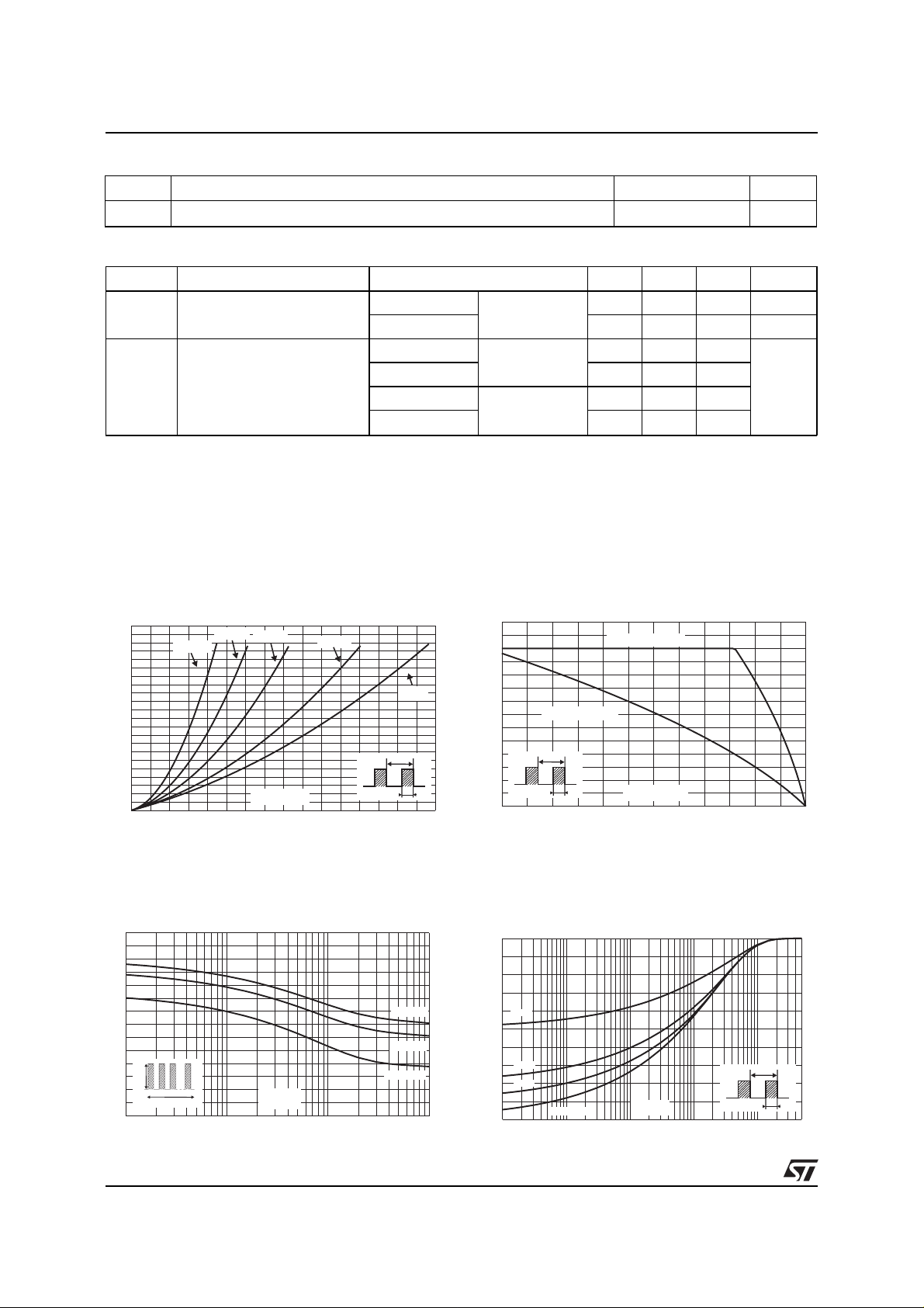
Fig. 1:
Average forward power dissipation versus
average forward current.
PF(av)(W)
2.2
2.0
δ = 0.05
δ = 0.1
δ = 0.2
δ = 0.5
1.8
1.6
1.4
δ = 1
1.2
1.0
0.8
0.6
T
0.4
0.2
0.0
0.0 0.5 1.0 1.5 2.0 2.5 3.0 3.5 4.0
Fig. 3:
Non repetitive surge peak forward current
IF(av) (A)
δ
=tp/T
tp
versus overload duration (maximum values).
IM(A)
14
12
10
8
6
4
I
M
2
0
1E-3 1E-2 1E-1 1E+0
t
δ
=0.5
t(s)
Ta=25°C
Ta=50°C
Ta=100°C
Fig. 2:
Average forward current versus ambient
temperature (δ=0.5).
IF(av)(A)
3.5
3.0
Rth(j-a)=Rth(j-l)
2.5
2.0
Rth(j-a)=90°C/W
1.5
1.0
0.5
0.0
0 25 50 75 100 125 150
Fig. 4:
T
δ
=tp/T
tp
T amb(°C)
Relative variation of thermal impedance
junction to ambient versus puls e dur ation.
Zth(j-a)/Rth(j-a)
1.0
0.8
δ = 0.5
0.6
0.4
δ = 0.2
δ = 0.1
0.2
0.0
1E-2 1E-1 1E+0 1E+1 1E+2 5E+2
Single pulse
tp(s)
δ
=tp/T
T
tp
2/4

STPS3L25S
Fig. 5:
Reverse leakage current versus reverse
voltage applied (typical values).
IR(mA)
1E+2
Tj=150°C
1E+1
Tj=125°C
Tj=100°C
1E+0
1E-1
1E-2
1E-3
0 5 10 15 20 25
Fig. 7-1:
Forward voltage drop versus forward
Tj=25°C
VR(V)
current (maximum values, high level).
IFM(A)
50
Typical values
Tj=150°C
10
Tj=125°C
Tj=100°C
1
0.0 0.2 0.4 0.6 0.8 1.0 1.2 1.4 1.6 1.8
VFM(V)
Tj=25°C
Fig. 6:
Junction capacitance versus reverse
voltag e applie d ( typical values) .
C(pF)
500
F=1MHz
Tj=25°C
100
VR(V)
10
12 5102030
Fig. 7-2:
Forward voltage drop versus forward
current (maximum values, low level).
IFM(A)
5.0
4.5
4.0
3.5
3.0
2.5
2.0
1.5
1.0
0.5
0.0
0.1 0.2 0.3 0.4 0.5 0.6
Typical values
Tj=150°C
Tj=125°C
Tj=25°C
Tj=100°C
VFM(V)
Fig. 8:
Thermal resistance junction to ambient
versus copper surface under each lead (Epoxy
printed circuit board FR4, copper thickness:
Rth(j-a) (°C/W)
100
90
80
70
60
50
40
30
20
0.0 0.5 1.0 1.5 2.0 2.5 3.0 3.5 4.0 4.5 5.0
S(Cu) (cm²)
3/4

STPS3L25S
PACKAGE ME CHANICAL D AT A
SMC
DIMENSIONS
E1
E
C
L
E2
FOOT PRINT DIMENSIONS
D
A1
A2
(in millimeters)
3.3
REF.
Millimeters Inches
Min. Max. Min. Max.
A1 1.90 2.45 0.075 0.096
A2 0.05 0.20 0.002 0.008
b 2.90 3.2 0.114 0. 126
c 0.15 0.41 0.006 0.016
E 7.75 8.15 0.305 0.321
E1 6.60 7.15 0.260 0.281
b
E2 4.40 4.70 0.173 0.185
D 5.55 6.25 0.218 0.246
L 0.75 1.60 0.030 0.063
2.0 4.2 2.0
Ordering type Marking Package Weight Base qty Delivery mode
STPS3L25S S23 SMC 0.243g 2500 Tape & reel
Band indicates cathode
Epoxy meets UL94,V0
Information furnished is believed to be accurate and reliable. However, STMicroelectronics assumes no responsibility for the consequences of
use of such information nor for any infringement of patents or other rights of third parties which may result from its use. No license is granted by
implication or oth erwise under any patent or patent rights of STMi croelectronics . Specifications mentioned i n this publication are subjec t to
change without notice. This publication supersedes and replaces all information previously supplied.
STMicroelectr oni cs products are n ot au thorized for use as critical components in life support devi ces or systems wi t hout express written approval of STMicroelectronics.
The ST logo is a registered trademark o f STMicroelectron ics
© 1999 STMicroelectronics - Printed in Italy - All rights reserved.
STMicroelectronics GROUP OF COMPANIES
Australia - Brazil - China - Finland - France - Germany - Hong Kong - India - Italy - Japan - Malaysia
Malta - Morocco - Singapore - Spain - Sweden - Switzerland - United Kingdom - U.S.A.
http://www.st.com
4/4
 Loading...