

STD17NF03L
N-CHANNEL 30V - 0.038Ω - 17A - DPAK/IPAK
STripFET™ POWER MOSFET
TYPE V
DSS
STD17NF03L 30V <0.05
■ TYPICAL R
■ EXCEPTIONA L dv/d t CAPABILITY
■ APPLICATION ORIENTED CHARACTERIZATION
■ ADD SUFFIX “T4” FOR ORDERING IN TAPE &
(on) = 0.038Ω
DS
R
DS(on)
I
D
Ω
17A
REEL
■ ADD SUFFIX “-1” FOR ORDERING IN IPAK
VERSION
DESCRIPTION
This Power Mosfet is the latest development of S TMicroelectronics unique “Single Feat ure Size™” strip-
based process. The resulting transistor shows extremely high packing density for low on-resistance,
rugged avalance characteristics and less critical alignment steps therefore a remarkable manuf acturing reproducibility.
APPLICATIONS
■ DC-DC & DC-AC CONVERTERS
■ MOTOR CONTROL, AUDIO AMPLIFIERS
■ SOLENOID AND RELAY DRIVERS
■ AUTOMOTIVE ENVIRONMENT
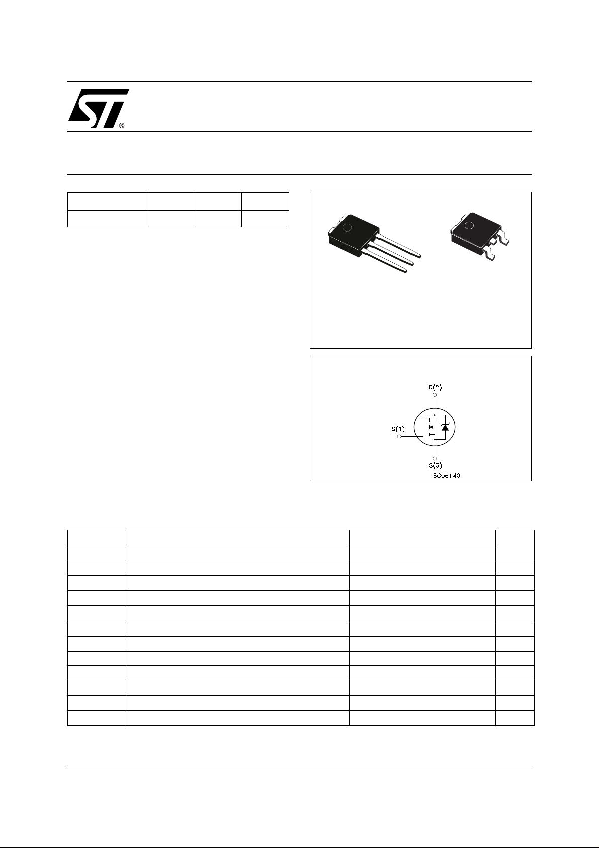
3
2
1
1
IPAK
DPAK
INTERNAL SCHEMATIC DIAGRAM
3
ABSOLUTE MAXIMUM RATINGS
Symbol Parameter Value Unit
V
DS
V
DGR
V
GS
I
D
I
D
I
DM
P
TOT
dv/dt (1) Peak Diode Recovery voltage slope 6 V/ns
E
AS
T
stg
T
j
(●) Pulse width limited by safe operating area
Drain-source Voltage (VGS = 0)
Drain-gate Voltage (RGS = 20 kΩ)
30 V
30 V
Gate- source Voltage ±20 V
Drain Current (continuos) at TC = 25°C
Drain Current (continuos) at TC = 100°C
(●)
Drain Current (pulsed) 68 A
Total Dissipation at TC = 25°C
17 A
12 A
20 W
Derating Factor 0.13 W/°C
(2)
Single Pulse Avalanche Energy 200 mJ
Storage Temperature –65 to 175 °C
Max. Operating Junction Temperature 175 °C
(1) ISD ≤17A, di/dt ≤300A/µs, VDD ≤ V
(2) Starting Tj=25°C, ID=11A, VDD=15V
(BR)DSS
, Tj ≤ T
JMAX.
1/9Aug 2000
STD17NF03L
THERMA L D ATA
Rthj-case Thermal Resistance Junction-case Max 7.5 °C/W
Rthj-amb Thermal Resistance Junction-ambient Max 62.5 °C/W
T
l
ELECTRICAL CHARACTERISTICS (TCASE = 25 °C UNLESS OTHERWISE SPECIFIED)
OFF
Symbol Parameter Test Conditions Min. Typ. Max. Unit
V
(BR)DSS
I
DSS
I
GSS
ON
(1)
Symbol Parameter Test Conditions Min. Typ. Max. Unit
V
GS(th)
R
DS(on)
I
D(on)
Maximum Lead Temperature For Soldering Purpose 275 °C
Drain-source
Breakdown Voltage
Zero Gate Voltage
Drain Current (V
GS
= 0)
Gate-body Leakage
Current (V
DS
= 0)
Gate Threshold Voltage
Static Drain-source On
Resistance
On State Drain Current
= 250 µA, VGS = 0
I
D
= Max Rating
V
DS
V
= Max Rating, TC = 125 °C
DS
= ±20V
V
GS
V
= VGS, ID = 250µA
DS
= 10V, ID = 8.5 A
V
GS
VGS = 5 V, ID = 8.5 A
V
> I
D(on)
x R
DS(on)max,
DS
VGS=10V
30 V
1µA
10 µA
±100 nA
1V
0.038 0.05
0.045 0.06
17 A
Ω
DYNAMIC
Symbol Parameter Test Conditions Min. Typ. Max. Unit
> I
(1)
g
fs
C
iss
C
oss
C
rss
Forward Transconductance
Input Capacitance
Output Capacitance 90 pF
Reverse Transfer
Capacitance
D(on)
x R
DS(on)max,
V
DS
ID=1 1A
VDS = 25V, f = 1 MHz, VGS = 0
7S
330 pF
40 pF
2/9
STD17NF03L
ELECTRICAL CHARACTERISTICS (CONTINUED)
SWITCHING ON
Symbol Parameter Test Conditions Min. Typ. Max. Unit
V
t
d(on)
Q
Q
Q
t
r
g
gs
gd
Turn-on Delay Time
Rise Time 100 ns
Total Gate Charge
Gate-Source Charge 3.6 nC
Gate-Drain Charge 2 nC
SWITCHING OFF
Symbol Parameter Test Conditions Min. Typ. Max. Unit
t
d(off)
t
r(off)
t
f
t
f
t
c
Turn-off-Delay Time
Fall Time 22 ns
Off-voltage Rise Time
Fall Time (see test circuit, Figure 5) 55 ns
Cross-over Time 75 ns
SOURCE DRAIN DIODE
Symbol Parameter Test Conditions Min. Typ. Max. Unit
I
SD
I
SDM
VSD (2)
t
rr
Q
rr
I
RRM
Note: 1. Pulsed: Pu l se duration = 300 µs, duty cyc l e 1.5 %.
2. Pulse width li mited by safe operating ar ea.
Source-drain Current 17 A
(1)
Source-drain Current (pulsed) 68 A
Forward On Voltage
Reverse Recovery Time
Reverse Recovery Charge 18 nC
Reverse Recovery Current 1.2 A
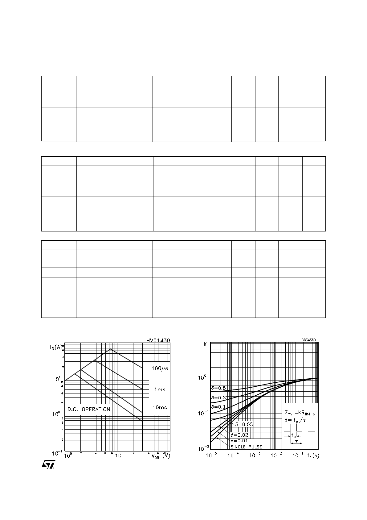
Safe Operating Area
= 15V, ID = 8.5A
DD
R
= 4.7Ω VGS = 4.5V
G
(see test circuit, Figure 3)
V
= 24V, ID = 17A,
DD
VGS = 10V
VDD = 15V, ID = 8.5A,
RG=4.7Ω, V
GS
= 4.5V
(see test circuit, Figure 3)
Vclamp =24V, I
R
=4.7Ω, V
G
GS
=17A
D
= 4.5V
ISD = 17A, VGS = 0
ISD = 17A, di/dt = 100A/µs,
VDD = 15V, Tj = 150°C
(see test circuit, Figure 5)
Ther m al Imp e d ence
11 ns
6.5 9 nC
25 ns
22 ns
1.5 V
30 ns
3/9

STD17NF03L
Output Characteristics
Transconductance
Transfer Characteristics
Static Drain-source On Resistance
Gate Charge vs Gate-source Voltage Capacitance Variations
4/9

STD17NF03L
Normalized Gate Thereshold Voltage vs Temp. Normalized On Resistance vs Temperature
Source-drain Diode Forward Characteristics
5/9

STD17NF03L
Fig. 2: Unclamped Inductive WaveformFig. 1: Unclamped Inductive Load Test Circuit
Fig. 3: Switching Times Test Circuit For
Resistive Load
Fig. 5: Test Circuit For Inductive Load Switching
And Diode Recovery Times
Fig. 4: Gate Charge test Circuit
6/9

TO-252 (DPAK) MECHANICAL DATA
STD17NF03L
DIM.
A 2.20 2.40 0.087 0.094
A1 0.90 1.10 0.035 0.043
A2 0.03 0.23 0.001 0.009
B 0.64 0.90 0.025 0.035
B2 5.20 5.40 0.204 0.213
C 0.45 0.60 0.018 0.024
C2 0.48 0.60 0.019 0.024
D 6.00 6.20 0.236 0.244
E 6.40 6.60 0.252 0.260
G 4.40 4.60 0.173 0.181
H 9.35 10.10 0.368 0.398
L2 0.8 0.031
L4 0.60 1.00 0.024 0.039
V2 0
MIN. TYP. MAX. MIN. TYP. MAX.
o
mm inch
o
8
o
0
o
0
P032P_B
7/9

STD17NF03L
TO-251 (IPAK) MECHANICAL DAT A
DIM.
MIN. TYP. MAX. MIN. TYP. MAX.
mm inch
A 2.2 2.4 0.086 0.094
A1 0.9 1.1 0.035 0.043
A3 0.7 1.3 0.027 0.051
B 0.64 0.9 0.025 0.031
B2 5.2 5.4 0.204 0.212
B3 0.85 0.033
B5 0.3 0.012
B6 0.95 0.037
C 0.45 0.6 0.017 0.023
C2 0.48 0.6 0.019 0.023
D 6 6.2 0.236 0.244
E 6.4 6.6 0.252 0.260
G 4.4 4.6 0.173 0.181
H 15.9 16.3 0.626 0.641
L 9 9.4 0.354 0.370
L1 0.8 1.2 0.031 0.047
L2 0.8 1 0.031 0.039
H
8/9
A
C2
L2
E
B2
= =
= =
D
B3
2
1 3
L1
A1
L
B6
C
A3
B
B5
G
= =
0068771-E

STD17NF03L
Information furnished is believed to be accurate and reliable. However, STMicroelectronics assumes no responsibility for the consequences
of use of such informa tion n or for an y infring ement of patent s or other rig hts of third part ies which may resu lt from its use . No l i cen se i s
granted by implication or otherwise under any pa tent or patent rights of STM icroelectronics. Specification mentioned in this publication are
subject to change without notice. This publication supersedes and replaces all information previously supplied. STMicroelectronics products
are not authorized for use as critical compo nents in life support devices or systems without express written approval of STMicroelectronics.
Australia - Brazil - China - Finland - France - Germany - Hong Kong - India - Italy - Japan - Malaysia - Malta - Morocco -
The ST logo is a trademark of STMicroelectronics
© 2000 STMicroelectronics – Printed in Italy – All Rights Reserved
STMicroelectronics GROUP OF COMPANIES
Singapore - Spain - Sweden - Switzerland - United Kingdom - U.S.A.
http://www.st.com
9/9
 Loading...