

SGS Thomson Microelectronics START540TR, START540 Datasheet
• LOW NOISE FIGURE: NFmin = 0.9dB
@ 1.8GHz, 5mA, 2V
• HIGH OUTPUT IP3 = 24dBm
@ 1.8GHz, 20mA, 2V
• GOOD RUGG ED NESS BVceo = 4.5 V
• TRANSITION FRE QU E NC Y 45 GHz
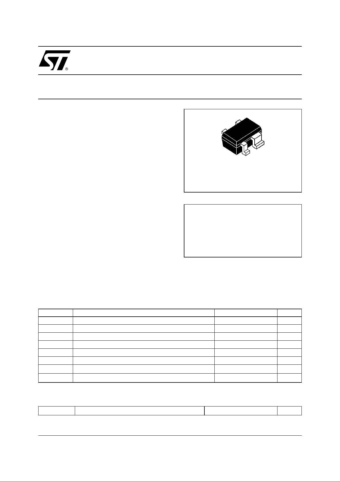
• ULTRA MINIATURE SOT343 PACKAGE
START540
NPN Silicon RF Transistor
SOT343 (SC70)
ORDER CODE
START540TR
BRANDING
540
DESCRIPTION
The START540 is a member of the START family
that provide the market with the state of the art of RF
silicon process. Manufacturated in the third
generation of ST proprietary bipolar process, it
APPLICATIONS
• LNA FOR GSM/DCS, DECT, PDC, PCS,
PCN, CDMA, W-CDMA
• GENERAL PURPOSE 500MHz-5GHz
offers the highest linearity with excellent Noise
Figure for 4.5V breakdown voltage(BVceo).
It reaches performance level only achieved with
GaAs products before.
ABSOLUTE MAXIMUM RATINGS
Symbol Parameter Value Unit
V
ceo
V
cbo
V
ebo
I
c
I
b
P
tot
T
stg
T
j
Collector emitter voltage 4.5 V
Collector base voltage 15 V
Emitter base voltage 1.5 V
Collector current 40 mA
Base current 4 mA
Total dissipation, Ts = 101
Storage temperature -65 to 150
Max. operating junction temperature 150
180 mW
o
C
o
C
ABSOLUTE MAXIMUM RATINGS
R
thjs
Thermal Resistance Junction soldering point 270
o
C/W
1/7July, 3 2002
START540
w
ELECTRICAL CHARACTERISTICS (Tj=25 oC,unless otherwise specified)
Symbol Parameter Test Conditions Min. Typ. Max. Unit
I
cbo
I
ebo
Hfe DC current gain Ic = 20mA, Vce = 3V 100 160
NFmin Minimim noise figure
Ga NFmin associated gain Ic = 5mA, Vce = 2V, f = 1.8GHz 16 dB
|S21|
Gms
P
-1dB
OIP3
Note(1) : Gm s = | S21 / S12 |
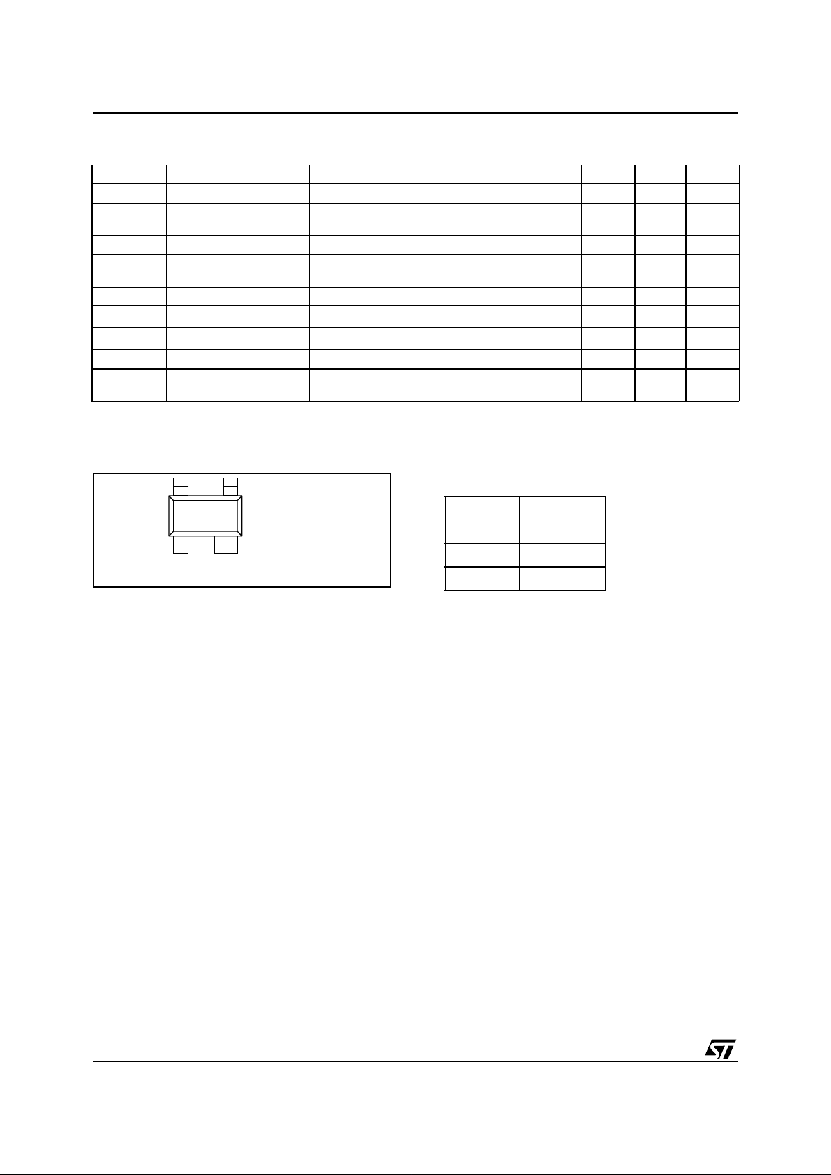
PINOUT
Collector cutoff current Vcb = 5V, Ie = 0A 150 nA
Emitter-base cutoff
current
2
(1)
Insertion power gain Ic = 20mA, Vce = 2V, f = 1.8GHz 19.5 dB
Maximum stable gain Ic = 20mA, Vce = 2V, f = 1.8GHz 22.7 dB
1dB compression point Ic = 20mA,Vce = 2V, f = 1.8GHz 13 dBm
Ouput third order
intercept point
4
3
Top vie
12
SOT343
Veb = 1.5V, Ic = 0A 15 µA
Ic = 5mA, Vce = 2V, f = 1.8GHz,
Ic = 20mA,Vce = 2V, f = 1.8GHz 24 dBm
Z
s
= Zsopt
0.9 dB
PIN CONNECTION
Pin No. Description
1BASE
3 COLLECTOR
2,4 EMITTER
2/7

COMMON EMITTER S-PARAMETERS ( VCE = 2V, IC = 20mA )
START540
f
S
11
S
21
S
12
GHz MAG ANG MAG ANG MAG ANG MAG ANG
0.1 0.699 -21.6 42.32 164.0 0.009 8 8.9 0.942 -12.2
0.5 0.545 -89.7 27.82 119.9 0.027 5 8.1 0.642 -50.6
0.9 0.480 -130.0 18.42 98.1 0.0 36 48.1 0.431 -70.6
1 0.476 -137.4 16.86 94.0 0.0 38 47.2 0.397 -74.7
1.5 0.483 -166.9 11.63 76.9 0.0 48 41.6 0.272 -96.2
1.8 0.494 179.6 9.63 68. 2 0.052 38.8 0.220 -110.7
2 0.503 172.2 8.49 63. 1 0.055 36.7 0.193 -123.3
2.5 0.513 157.6 6.46 53. 6 0.061 31.7 0.148 -154.4
3 0.533 147.8 5.34 45. 9 0.069 26.7 0.142 -171.4
3.5 0.551 139.6 4.54 36. 6 0.077 21.2 0.153 177.9
4 0.559 133.8 3.87 28. 3 0.085 13.7 0.154 162.7
COMMON EMITTER S-PARAMETERS ( VCE = 2V, IC = 5mA )
f
S
11
GHz MAG A NG MAG ANG MAG ANG MAG ANG
0.5 0.816 -50.5 14.56 140.8 0.038 6 5.8 0.879 -30.3
S
21
S
12
S
22
S
22
0.9 0.715 -84.6 11.92 118.2 0.058 4 8.4 0.720 -49.0
1 0.695 -92.5 11.32 113.2 0.061 4 5.0 0.685 -53.1
1.5 0.620 -128.0 8.64 91. 5 0.075 30.9 0.515 -71.9
1.8 0.589 -145.6 7.39 80. 9 0.080 23.8 0.425 -81.8
2 0.581 -156.1 6.66 74. 5 0.080 19.3 0.374 -88.4
2.5 0.570 -167.6 5.87 8.0 0.082 14.8 0.316 -96.8
3 0.572 167.6 4.37 51. 7 0.085 5.7 0.225 -166.8
3.5 0.585 155.3 3.74 40. 4 0.090 1.1 0.208 -128.4
4 0.592 146.1 3.20 30. 6 0.094 -5.0 0.184 -141.2
COMMON EMITTER NOISE-PARAMETERS ( VCE = 2V, IC = 5mA )
f
F
min
Γ
opt
R
n
r
n
GHz dB MAG ANG Ω -dBdB
1.8 0.91 0.39 100.8 6.4 0.128 17.38 1.12
2 0.96 0.48 115.2 6.38 0.127 16.47 1.22
2.5 1.01 0.48 136.8 5.94 0 .118 14.35 1.34
3 1.14 0.46 163 5.6 0 .112 12.82 1.38
3.5 1.3 0.39 -160 5.2 0.104 11.46 1.42
4 1.4 0.32 -122.4 5 0.1 10.12 1.66
|S21|
2
F
50
3/7
 Loading...