


• HIGH EFFICIENCY
• HIGH GAIN
• LINEAR AND NON LINEAR OPERATION
• TRANSITI ON FR E QU E NC Y 42 GHz
• ULTRA MINIATURE SOT343 (SC70) PACKAGE
DESCRIPTION
START499 is a product of the START family that
provide the market with a Si state-of-art RF process.
Manufactured in St 3rd generation bipolar process, it
offers the highest power, gain and efficiency in
SOT343 for given breakdown voltage (BVceo).
Suitable for a wide range of applications up to 5GHz,
it shows a performance level achieved before wi th
GaAs products only.
START499
NPN Silicon RF Transistor
SOT343 (SC70)
ORDER CODE
START499TR
APPLICATIONS
• PA FOR DECT OR PHS
• PA STAGE FOR WIRELESS LAN AND
BLUETOOTH @ 2.5GHz
• UHF-VHF PRE POWER AMPL IFIER
BRANDING
499
ABSOLUTE MAXIMUM RATINGS
Symbol Parameter Value Unit
V
ceo
V
cbo
V
ebo
I
c
I
b
P
tot Total dissipation at T
T
stg
T
j
Collector emitter voltage 4.5 V
Collector base voltage 15 V
Emitter base voltage 1.5 V
Collector current 600 mA
Base current 32 mA
= 60 oC
S
Storage temperature -65 to 150
Max. operating junction temperature 150
600 mW
ABSOLUTE MAXIMUM RATINGS
R
thjs
Thermal Resistance Junction soldering point 150
o
C/W
o
C
o
C
1/7July, 3 2002
START499
w
ELECTRICAL CHARACTERISTICS (Tj=25 oC,unless otherwise specified)
Symbol Parameter Test Conditions Min. Typ. Max. Unit
I
cbo
I
ebo
Hfe DC current gain Ic = 160mA, Vce = 4V 160
G Power gain Ic =200mA, Vce = 3V, f = 1.8GHz 15 dB
P
-1dB
IP3
NF Noise Figure Ic = 200mA,Vce = 3V, f = 1.8GHz 3.3 dB
QUICK REFERENCE DATA
MODE OF OPERATION
Class-AB (Icq = 5mA) 1.9 3.6 26 ≥12 typ. 68
Collector cutoff current Vcb = 5V, Ie = 0A 1.2 µA
Emitter-base cutoff
current
1dB compression point Ic = 200mA,Vce = 3V, f = 1.8GHz 23.5 dBm
Ouput third order
intercept point
Veb = 1.5V, Ic = 0A 120 µA
Ic = 200mA,Vce = 3V, f = 1.8GHz 33.5 dBm
f
(GHz)
V
(V)
CE
P
L
(dBm)
G
(dB)
P
(%)
η
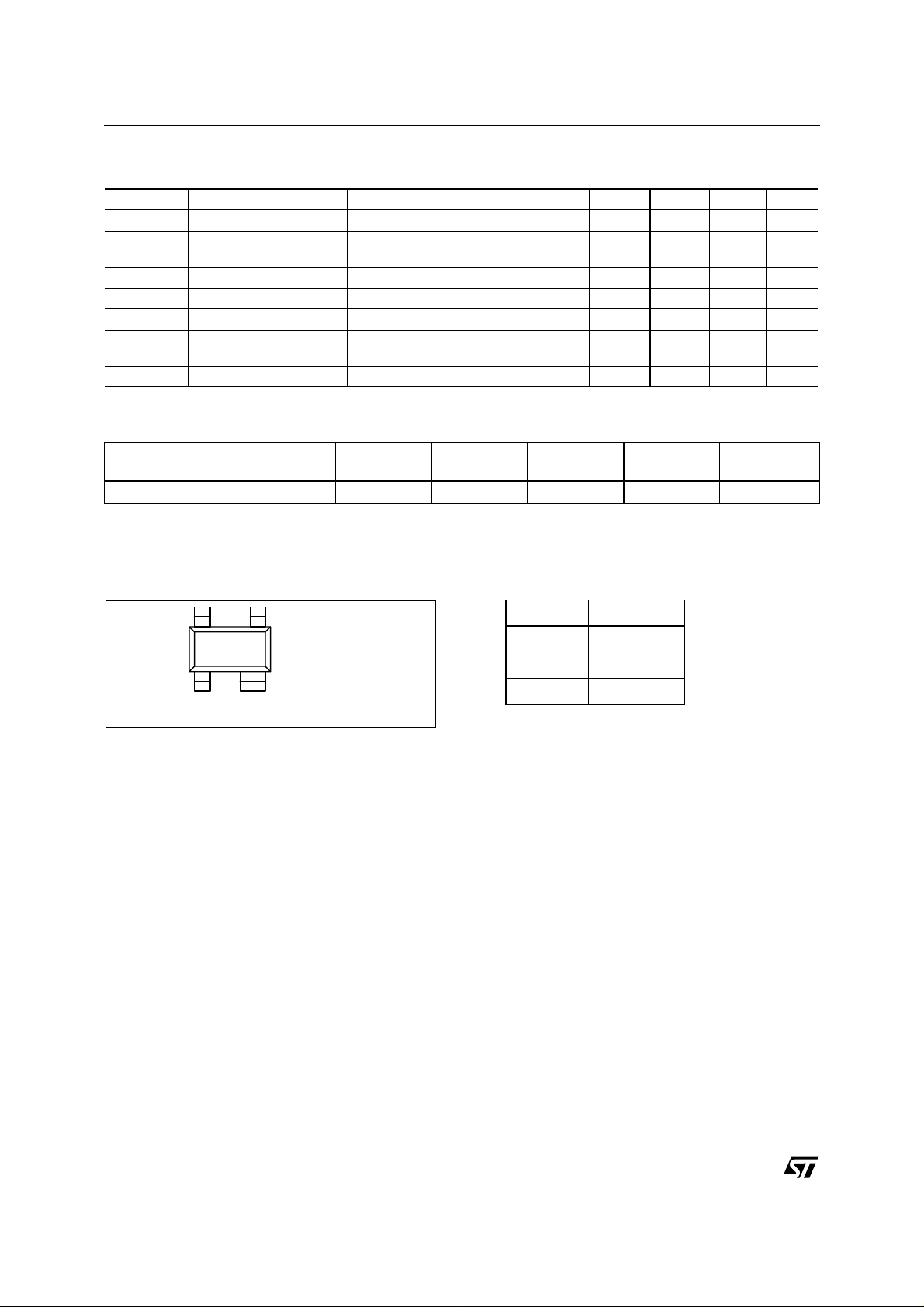
PINOUT
4
12
SOT343
PIN CONNECTION
3
Top vie
Pin No. Description
1 BASE
3 COLLECTOR
2,4 EMITTER
2/7
SPICE PARAMETERS (Gummel-Poon Model, Berkley-SPICE 2G.6 Syntax)
TRANSISTOR CHIP DATA
Symbol Value Symbol Value Symbol Value
TMEAS 27.0 FC 0.81 XJBC 0.51
IS 3.27E-16 EG 1.12 XTI 3.68
ISE 13.08E-12 NF 1 BF 332
NR 1 NE 3.2 VAF 70
ISC 7.89E-15 BR 9.75 VAR 2.1
o
IKF
TR 7E-10 PTF 38 VTF 29.7
XTF 16.3 ITF 5.01 MJE 0.341
RB 2.58 RBM 0.83 MJC 0.312
RC 0.597 RE 0.066 MJS 0.297
CJE 3048E-15 VJE 1.09 IKR 57.3E-3
CJC 930E-15 VJC 0.695 XTB -0.82
CJS 510E-15 VJS 0.507
{3.948*((T(
C)+273.15)/
300.15)^(-1.7)}
NC 1.5 TF 3.4E-12
PACKAGE EQUIVALENT CIRCUIT
C2
C2
C=30 fF
C=30 fF
START499
L4
.
.
B .
B .
L4
L=0.5 nH
L=0.5 nH
B’ C’
B’ C’
L3 L5 L6
L3 L5 L6
L=0.1 nH
L=0.1 nH
C1
C1
Transistor
Transistor
Chip
Chip
E’
E’
L=0.15 nH
L=0.15 nH
L1
L1
.
.
L=0.05 nHL2
L=0.05 nHL2
.
.
E
E
..
L=0.1 nH L=0.5 nH
L=0.1 nH L=0.5 nH
C3
C3
C=780 fFC=640 fF
C=780 fFC=640 fF
..
C
C
In order to avoid high complexity of the package equivalent circuit, the two emitter leads of SOT-343
package are combined in one electrical connection.
FOR MORE ACCURACY SIMULATION IN SATURATION REGION :
Adding the 5 Spice parameters showed in Table A and using ST Spice Library (available on request) you
can achieve a more accuracy simulation in the saturation region. ST Spice library is compatible with
following simulators: ELDO MENTOR (any version), SPECTRE CADENCE (any version), ADS (version
2001 only).
Table A (Spice Parameters extracted in saturation region)
RW Vjj ENP VRP RP
1.034 0.755 2.235 {7.2*((TEMPER+273.15)/300.15)^(0.125)} 0.33E-6
3/7
 Loading...