70+70W STEREO POWER AMPLIFIER
■
MONOCHIP BRIDGE STEREO AMPLIFIER
FOR BASH
■
55+55W OUTPUT POWER @ RL = 4/8
THD = 0.5%
■
70+70W OUTPUT POWER @ RL = 4/8
THD = 10%
■
HIGH DYNAMIC PREAMPLIFIER INPUT
STAGES
■
EXTERNAL PROGRAMMABLE FEEDBACK
TYPE COMPRESSORS
■
AC COUPLED INPUT TO CLASS AB BRIDGE
OUTPUT AMPLIFIER
■
PRECISION RECTIFIERS TO DRIVE THE
DIGITAL CONVERTER
■
ON-OFF SEQUENCE/ TIMER WITH MUTE
AND STANDBY
■
PROPORTIONAL OVER POWER OUTPUT
CURRENT TO LIMIT THE DIGITAL
CONVERTER
■
ABSOLUTE POWER BRIDGE OUTPUT
®
ARCHITECTURE
Ω,
Ω,
STA550
FLEXIWATT27
TRANSISTOR POWER PROTECTION
■
ABSOLUTE OUTPUT CURRENT LIMIT
■
INTEGRATED THERMAL PROTECTION
■
POWER SUPPLY OVER VOLTAGE
PROTECTION
■
FLEXIWATT POW ER PAC KAG E WI TH 2 7 PIN
■
BASH® LICENCE REQUIRED
DESCRIPTION
The STA550 is a fully integrated power module designed to implement a BASH® amplifier when used
in conjunction with STABP01 digital processor.
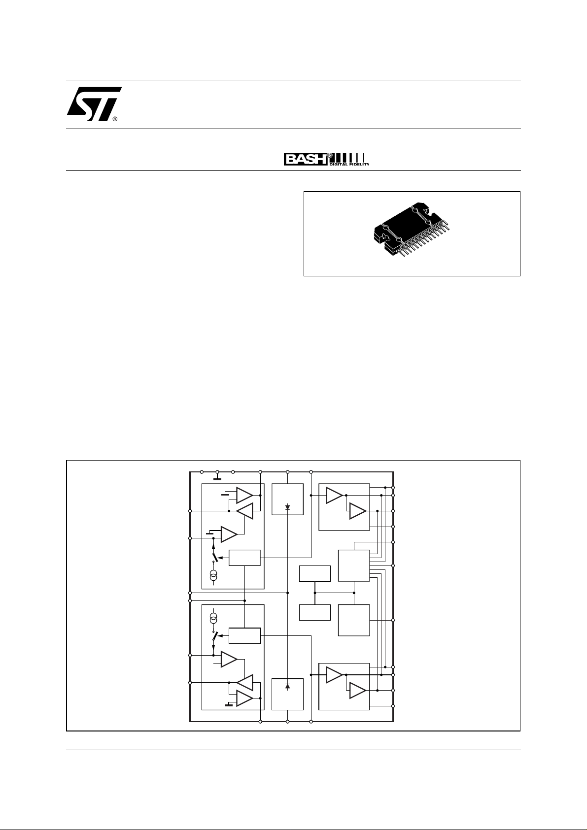
BLOCK DIAGRAM
IN_PRE1
ATT_REL1
TRK_OUT
THRESH
ATT_REL2
IN_PRE2
COMPRESSOR
V/l
S1
Ict
Ict
S1
V/l
COMPRESSOR
-VSGND+VS
+
-
PEAK/2
DETECTOR
PEAK/2
DETECTOR
-
+
PWR_INP1TRK_1OUT_ PRE1
D01AU1263
CD+1
OUT1+
OUT1-
CD-1
CD+
PROT.
STBY/MUTE
CD+2
OUT2+
OUT2-
ABSOLUTE
VALUE
BLOCK
∆G
PROTECTION
PROTECTION
∆G
ABSOLUTE
VALUE
BLOCK
TRK_2OUT_ PRE2
PWR_INP2
+2
-1
OUTPUT BRIDGE
SOA
VOLTAGE
THERMAL
DETECTOR
TURN-
ON/OFF
SEQUENCE
+2
-1
OUTPUT BRIDGE CD-2
July 2003
1/16

STA550
DESCRIPTION
(continued)
Notice that normally only one Digital Converter is needed to supply a stereo or multi-channel amplifier system,
therefore most of the functions implemented in the circuit have summing outputs
The signal circuits are bias ed by fixed negative and posi tive voltages r eferred to Ground. Instead the final stages of the output amplifiers are supplied by two external voltages that are following the audio signal . In this way
the headroom for the output transistors is kept at minimum level to obtain a high efficiency power amplifier.
The Compressor circuits, one for each channel, performs a particular transfer behavior to avoid the dynamic
restriction that an adaptive system like this requires. To have a high flexibility the attack / release time and the
threshold levels are exter nal ly progr ammable. The tracking s ignal for the ex ter nal digita l converter is generated
from the Absolute Value block that rectifies the audio signal present at the compressor output. The outputs of
these blocks are decoupled by a diode to permit an easy sum of this signal for the mult ichannel application. The
output power bridges have a dedicated input pin to perform an AC decoupling to cancel the compressor output
DC offset. The gain of the stage is equal to 4 (+12dB). A sophis ticated circuit performs the output transistor power detector that , with the digital converter, reduces the power supply voltage . Moreover, a maximum current
output limiting and the over temperature sensor have been added to protect the circuit itself. The external voltage applied to the STBY/MUTE pin forces the two amplifiers in the proper condition to guarantee a silent turnon and turn-off.
ABSOLUTE MAXIMUM RATINGS
Symbol Parameter Value Unit
+V
-V
Positive supply voltage referred to pin 13 (GND) 30 V
s
Negative supply voltage referred to pin 13 (GND) -24 V
s
V
CD+
V
CD+
V
CD-
V
CD-
V
Att_Rel1
V
Att_Rel2
V
Pwr_Imp1
V
Pwr_Imp2
V
Trk_1
V
Trk_2
V
In_pre1
V
In_pre2
V
threshold
Positive supply voltage tracking rail referred to pin 13 (GND) 22 V
Positive supply voltage operated to Vs+
Negative supply voltage referred to -Vs
Negative supply voltage tracking rail referred to pin 13 (GND) -22 V
Pin 3, 25 Negative & Positive maximum voltage referred to GND
(pin 13)
Pin 7, 21, 18, 10 Negative & Positive maximum voltage referred
to GND (pin 13)
Pin 8, 20 Negative & Positive maximum voltage referred to GND
(pin 13)
Pin 17 Negative & Positive maximum voltage referred to GND
(pin 13)
I
stb-max
V
stbymute
I
OUT
Note 1: V
Note 2: All pin s wi t h s tand ±2KV ESD but not pin 11
Pin 11 maximum input current (Internal voltage clamp at 5V) 500 µA
Pin 11 negative maximum voltage referred to GND (pin 13) -0.5 V
Output Current 7.0 A
must not be more negative than -Vs and V
CD-
(1)
(1)
must not be more positive than +V
CD+
0.3 V
-0.3 V
-0.5 to +20 V
-20 to +20 V
-0.5 to +0.5 V
-7 to +0.5 V
S
2/16

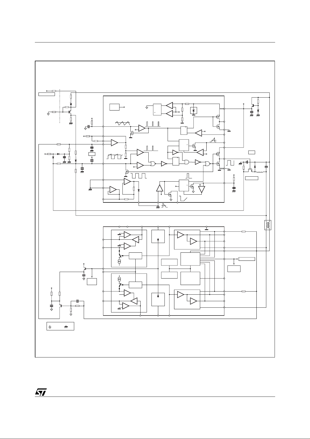
Figure 1. Connection Diagram between STA550 and STAbp01
490
PROTECTION
+10V
10K
490
EMI BARRIER
OPTIONAL
2K
2200pF
2.67K
4.99K
6.82K
2K
1K
10V
CD+
100K
1K
499K
GATE
CURRENT_SENSE
680pF
BUFFER IN
BUFFER OUT
CLOCK
COMP
10pF
FA IN
STABP01
VREF
1V
250Hz
10
4
ERROR
3
V
FB
V+
2
5
19
20
1
AMP
+
COMP/3
DISCHARGE
(RESET)
TRANSISTOR
BUFFER
+
-
2R
+
-
R
1V
1V
CURRENT SENSE
COMPARATOR
+
R
+
-
1V
R17
18
REC_OUT
INTERNAL
CIRCUIT
+
-
FAST ATTACK
CONTROL
UVLO: 7V = on
5V = off
-
R
Q
Q
ON
16 17
ONE SHOT DUTY ACCEL
+
-
S
+
SQQ
R
PWM LATCH
ONE SHOT
--+
1V
1V
1V
SOFT SWITCH
SQR
CLKQD
RESET
SIGNAL
CLKDQ
RESET
STA550
POWER SUPPLY1
OUTPUT
GROUND1
SOFT SW RESET
DEAD TIME
POWER_VS2
OUTPUT
GROUND2
I
10V
ONE
SHOT
DELAY
SENSE
+10V
GATE
CD+
CD-
ISENSE
10V
14
13
1V
OPEN DRAIN
OUTPUT
12
11
1V
6
7
8
9
15
Q
Q
Q
1V
+
+
-
1V10V
+
+25V
95K
100pF
GND-AUDIO GND
-VS
+VS
2714
+
COMPRESSOR
S1
S1
COMPRESSOR
∆G
V/l
PEAK/2
DETECTOR
Ict
Ict
PEAK/2
DETECTOR
V/l
∆G
-
+
19 18 21
8
IN_PRE1
3
ATT_REL1
+25V
680pF
OTHER
STA575
TRK-OUT
15K
2.43K
1000pF
2.55K
TRK_OUT
THRESH
ATT_REL2
IN_PRE2
16
17
25
20
ABSOLUTE
VALUE
BLOCK
ABSOLUTE
VALUE
BLOCK
TRK_2OUT_ PRE2
PWR_INP1TRK_1OUT_ PRE1
VOLTAGE
PROTECTION
THERMAL
PROTECTION
PWR_INP2
+2
OUTPUT BRIDGE
DETECTOR
ON/OFF
SEQUENCE
+2
OUTPUT BRIDGE
SOA
TURN-
GND
137109
-1
-1
STA575
15
12
11
22
24
23
26
6
4
5
2
CD+1
OUT1+
OUT1-
CD-1
CD+
PROT.
OTHER
STA575
PROTECTION
STBY/MUTE
CD+2
OUT2+
OUT2-
CD-2
R
SENSE
PROTECTION
R
SENSE
EMI BARRIER
OPTIONAL
D02AU1391
3/16

STA550
THERMAL DATA
Symbol Parameter Value Unit
T
Max Junction temperature 150 °C
j
R
th j_case
Thermal Resistance Junction to case .............................. ..max 1 °C/W
OPERATING RANGE
Symbol Parameter Value Unit
+V
-V
∆V
V
CD+
V
CD-
I
in_Max
V
trheshold
T
amb
I
sb_max
Positive supply voltage +20 to +30 V
s
Negative supply voltage -10 to -22 V
s
Delta positive supply voltage 5V ≤ (Vs+ - VCD+) ≤ 10V V
s+
Positive supply voltage tracking rail +3 to 17 V
Negative supply voltage tracking rail -17 to -3 V
Current at pin In_Pre1, In_Pre2, related to compressor behaviour -1 to +1 mA peak
Voltage at pin Threshold -5 to 0 V
Ambient Temperature Range 0 to 70 °C
Pin 11 maximum input current (Internal voltage clmp at 5V) 200 µA
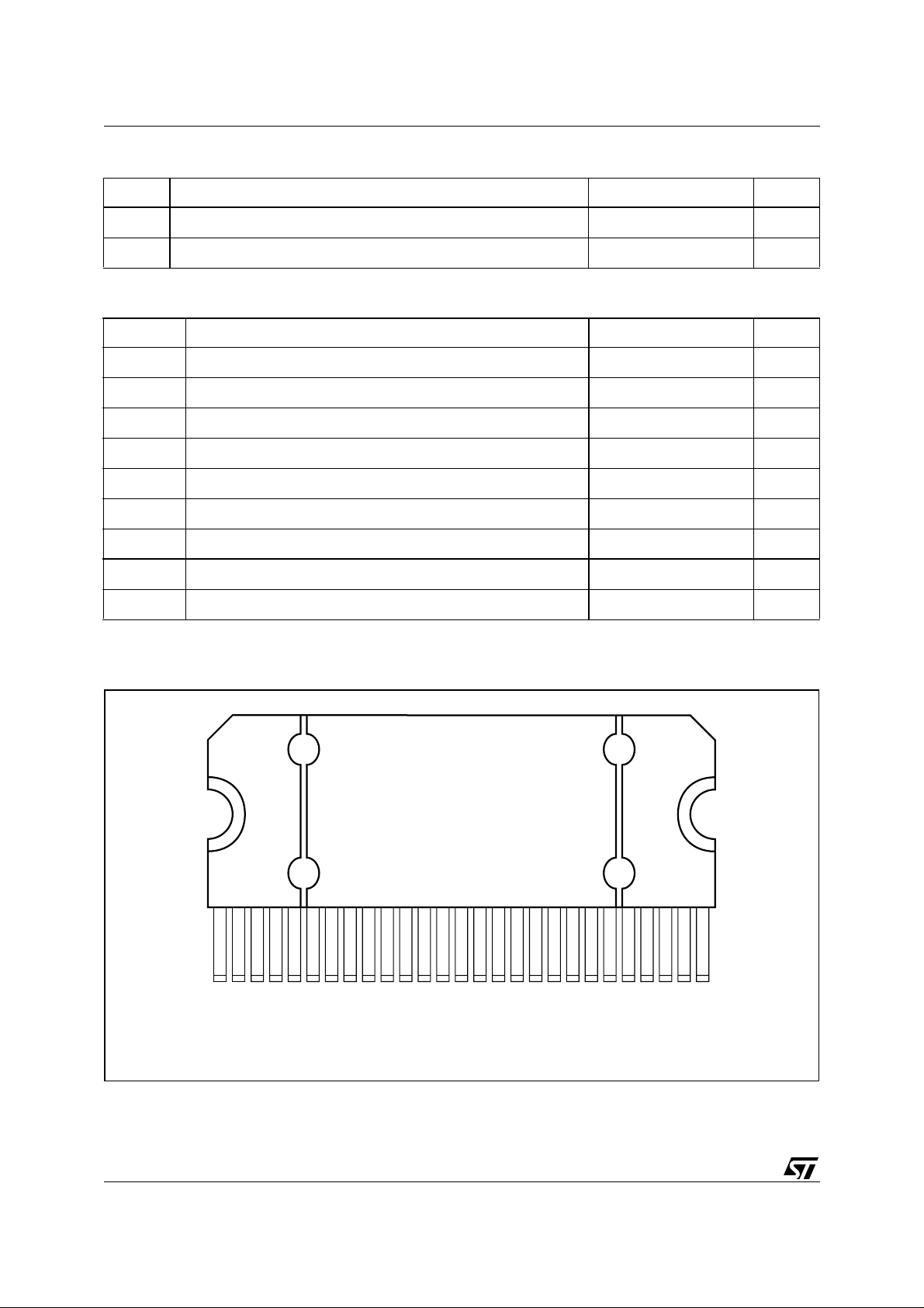
PIN CONNECTION
4/16
OUT2+
ATT_REL2
D01AU1251
27
CD-2
-Vs
1
-V
S
CD-1
ATT-REL1
OUT1-
OUT1+
CD+1
PWR_INP1
IN_PRE1
OUT_PRE1
TRK_1
STBY/MUTE
S
+V
CD+
GND
PROTECTION
TRK_2
TRK_OUT
THRESHOLD
IN_PRE2
PWR_INP2
OUT_PRE2
CD+2
OUT2-

PIN FUNCTION
N° Name Description
1 - Vs Negative Bias Supply
2 CD-1 Channel 1 Time varying tracking rail negative power supply
3 Att_Rel1 Attack release rate for channel 1
4 Out1+ Channel 1 speaker positive output
5 Out1- Channel 1 speaker negative output
6 CD+1 Channel 1 positive power supply
7 Pwr_Inp1 Input to channel 1 power stage
8 In_pre1 Pre-amp input for channel 1 (virtual ground)
9 Out_pre1 Output channel 1 pre-amp
10 Trk_1 Absolute value block input for channel 1
11 Stby/mute Standby/mute input voltage control
12 Protection Protection signal for STABP01 digital processor
13 Gnd Analog Ground
STA550
14 +Vs Positive Bias Supply
15 CD+ Time varying tracking rail positive power supply
16 Trk_out Reference output for STABP01 digital processor
17 Threshold Compressor threshold input
18 Trk_2 Absolute value block input for channel 2
19 Out_pre2 Output channel 2 pre-amp
20 In_pre2 Pre-amp input for channel 2 (virtual ground)
21 Pwr_Inp2 Input to channel 2 power stage
22 CD+2 Channel 2 positive power supply
23 Out2- Channel 2 speaker negative output
24 Out2+ Channel 2 speaker positive output
25 Att_Rel2 Attack release rate for channel 2
26 CD-2 Channel 2 Time varying tracking rail negative power supply
27 -Vs Negative Bias Supply
5/16
 Loading...