SGS Thomson Microelectronics STA500 Datasheet

30V 3.5A QUAD POWER HALF BRIDGE
■ MINIMUM INPUT OUTPUT PULSE WIDTH
DISTORTION
■ 200mΩ R
OUTPUT STA GE
■ CMOS COMPATIBLE LOGIC INPUTS
■ THERMAL PROTECT I O N
■ THERMAL WARNING OUTPUT
■ OVERVOLTAGE, UNDERVOLTAGE
PROTECTION
DESCRIPTION
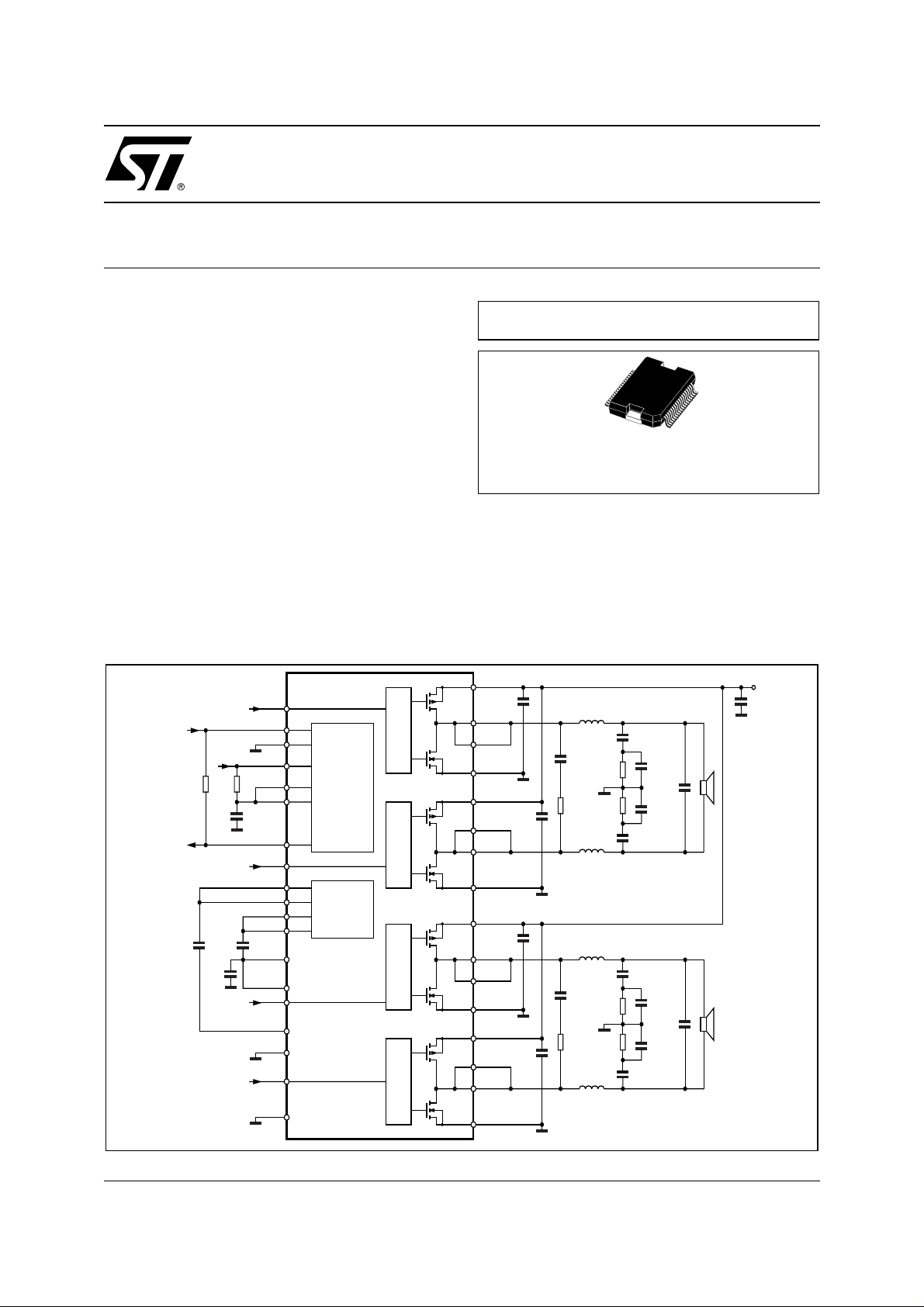
STA500 is a monoli thic quad half bridge stage in Multipower BCD Technology. The device can be us ed as
dual bridge or reconfigured, by connecting CONFIG
pin to Vdd pin, as single bridge with double current
capability, and as half bridge (Binary mode) with half
COMPLEMENTAR Y DM OS
dsON
STA500
MULTIPOWER BCD TECHNOLOGY
PowerSO36
ORDERING NUMBER: STA500
current capability.
The device is particulary de signed to mak e the output
stage of a stereo All-Digital High Efficiency (DDX™)
amplifier capable to deliver 30 + 30W output power
on 8
Ω
load and 60W on 8Ω load in bridge BTL con-
Ω
figuration or mono 60W on 4
have threshold proportional to Ibias pin voltage.
load. The input pins
AUDIO APPLICATION CIRCUIT (Dual BTL)
29
IN1A
+3.3V
TH_WAR
100nF
C58
R57
10K
C58
100nF
C60
100nF
R59
10K
C53
100nF
IN1A
TRI-STATE
IN1B
IN2A
GND-Clean
IN2B
IBIAS
CONFIG
PWRDNPWRDN
FAULT
TH_WAR
IN1B
V
V
V
V
VCCSIGN
V
SIGN
CC
IN2A
GND-Reg
IN2B 32
GNDSUB
DD
DD
SS
SS
23
24
25
27
26
28
30
21
22
33
34
35
36
31
20
19
1
PROTECTIONS
&
LOGIC
REGULATORS
M17
M15
M16
M14
1A
V
CC
15
M3
M2
M5
M4
C30
1µF
17
OUT1A
16
OUT1A
14
GND1A
12
V
1B
CC
OUT1B
OUT1B
GND1B
2A
V
CC
OUT2A
OUT2A
GND2A
V
2B
CC
OUT2B
OUT2B
GND2B
C32
1µF
C31
1µF
C33
1µF
11
10
13
7
8
9
6
4
3
2
5
L18 22µH
C52
330pF
R63
20
L19 22µH
L113 22µH
C109
330pF
R104
20
L112 22µH
D00AU1148B
C20
100nF
R98
6
R100
6
C21
100nF
C110
100nF
R103
6
R102
6
C111
100nF
C99
100nF
C23
470nF
C101
100nF
C107
100nF
C108
470nF
C106
100nF
+V
CC
C55
1000µF
July 2003
1/10

STA500
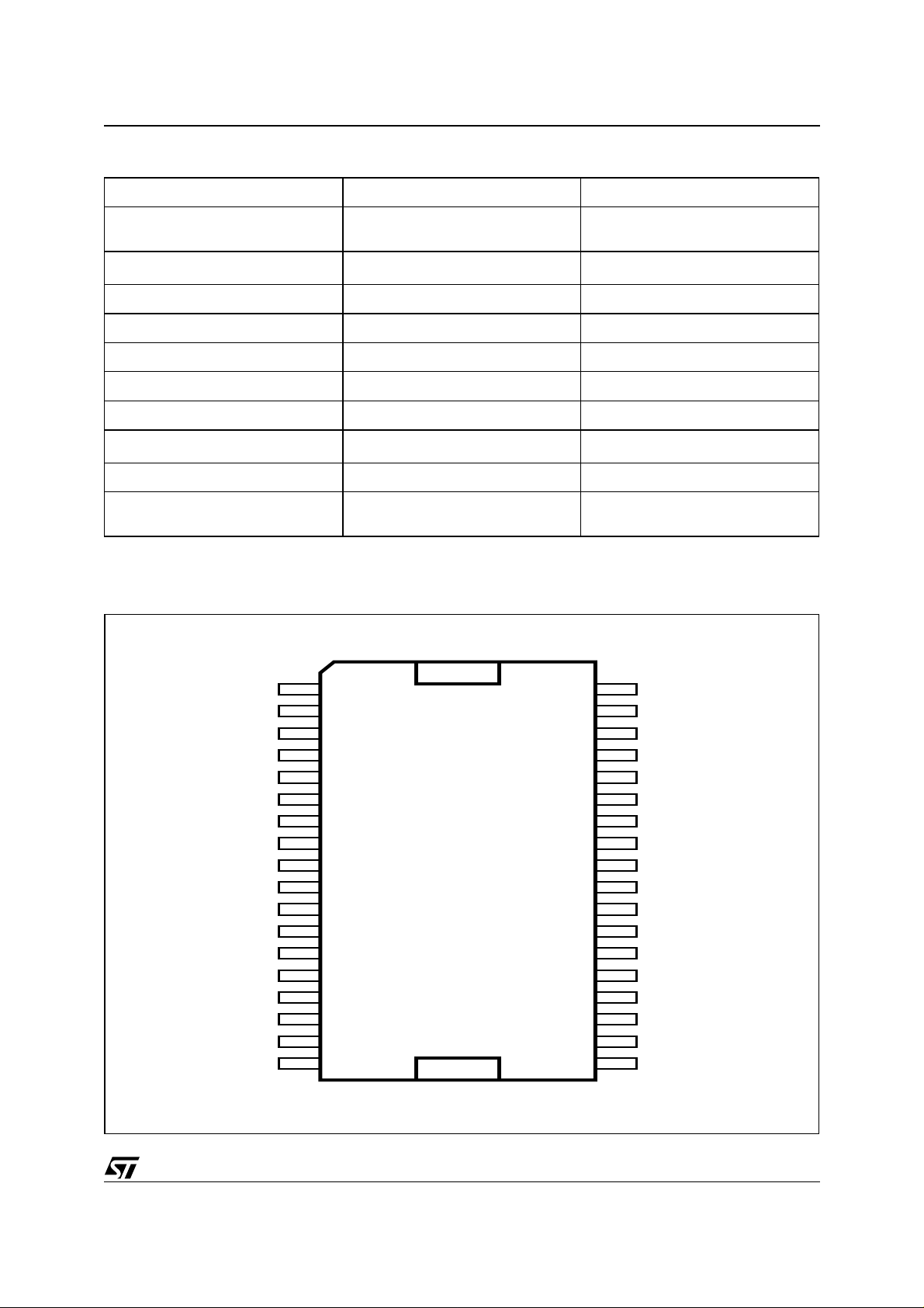
PIN FUNCTION
N° Pin Description
1 GND-SUB Substrate ground
35 ; 36 Vcc Sign Signal Positive supply
15 Vcc1A Positive Supply
12 Vcc1B Positive Supply
7 Vcc2A Positive Supply
4 Vcc2B Positive Supply
14 GND1A Negative Supply
13 GND1B Negative Supply
6 GND2A Negative Supply
5 GND2B Negative Supply
16 ; 17 OUT1A Output half bridge 1A
10 ; 11 OUT1B Output half bridge 1B
8 ; 9 OUT2A Output half bridge 2A
2 ; 3 OUT2B Output half bridge 2B
29 IN1A Input of half bridge 1A
30 IN1B Input of half bridge 1B
31 IN2A Input of half bridge 2A
32 IN2B Input of half bridge 2B
21 ; 22 Vdd 5V Regulator referred to ground
33 ; 34 Vss 5V Regulator referred to +Vcc
25 PWRDN Stand-by pin (Control input)
26 TRI-STATE Hi-Z pin (Control input)
27 FAULT Fault pin advisor (Open Collector Output)
24 CONFIG Configuration setting pin
28 TH-WAR Thermal warning advisor (Open Collector Output)
19 GND-clean Logical ground
23 IBIAS High logical state setting voltage
18 NC Not connected
20 GND-Reg Ground for Vdd regulator
2/10

FUNCTIONAL PIN STATUS
PIN NAME Logical value IC -STATUS
STA500
FAULT 0 Fault detected (Short circuit, or
FAULT
(*)
1 Normal Operati on
TRI-STATE 0 All powers in Hi-Z state
TRI-STATE 1 Normal operati on
PWRDN 0 Low absorpion
PWRDN 1 Normal operati on
THWAR 0 Temperature of the IC =130°C
THWAR
(*)
1 Normal operati on
CONFIG 0 Normal Operation
CONFIG
(*) : The pin is open collector. To have the high logic va l ue, it needs to be pulled up by a r esistor.
(**:) To put CONFIG = 1 mean s connect Pin 24 (CONFIG) to P i ns 21, 22 (Vdd)
(**)
1 OUT1A=OUT1B ; OUT2A=OUT2B
PIN CONNECTION
Thermal ..)
(IF IN1A = IN1B; IN2A = IN2B)
GND-SUB
OUT2B
OUT2B
2B
V
CC
GND2B
GND2A IN2A
V
2A
CC
OUT2A
OUT2A TH_WAR
OUT1B
OUT1B
V
1B
CC
GND1B
GND1A
V
1A
CC
OUT1A
OUT1A GND-Reg
N.C. GND-Clean
1
2
3
4
5
6
7
8
9
10 27
11
12
13 24
14
15
16
17
18
D00AU1133
36
35
34
33
32
31
30
29
28
26
25
23
22
21
20
19
V
VCCSign
V
V
IN2B
IN1B
IN1A
FAULT
TRI-STATE
PWRDN
CONFIG
IBIAS
V
V
CC
SS
SS
DD
DD
Sign
3/10
 Loading...