

SGS Thomson Microelectronics STA308 Datasheet

STA308
MULTICHANNEL DIGITAL AUDIO PROCESSOR WITH DDX™
PRODUCT PREVIEW
■ 8 DDX
■ From 32kHz to 192kHz Input Sample Rates
■ Volume Control from 0 to -100dB (0.5 dB steps)
■ Variable Digital Gain from 0 to 24dB (0.5dB
■ I2S Inputs and Outputs
■ Individual Channel and Master Gain/
■ Individual Channel Mute and Zero Input Detect
■ Selectable Serial Audio Data Interface
■ Bass/T re b le C on t r ols
■ Channel Mapping of any Input to any
■ Active Crossover Capability
■ DC Blocking Selectable High-Pass Filter
■ Selectable Bass Managemen t on Channel 6
■ Selectable Adjacent Channel Mixing Capabili ty
■ Selectable DDX
■ Selectable Clock Input Ratio
■ Selectable De-emphasis
■ Selectable DDX
■ AM Interference Reduction Mode
■ I2C Control
TM
Channels Capability (24 bit)
Supported
steps) with Digital Limiter Functionality and
Variable Attack and Release Time
Attenuation
Auto-Mute
Processing/DDX
TM
Channel
TM
Headphone Output on
Channels 7 & 8
TM
Ternary, or Binary PWM
output
TQFP64
ORDERING NUMBER: STA308
DESCRIPTION
The STA308 is a single chip solution for digital audio
processing and control in multi-channel applications.
It provides output capabilities for DDX
tal Amplification). In conjunction with a DDX
TM
(Direct Digi-
TM
power
device, it provides high-quality, high-efficiency, all
digital amplification. The device is extremely versatile
allowing for input of most digital formats including 6.1
channel and 192kHz, 24-bit DVD-Audio.
The internal 24-bit DSP allows for high resolution
processing at all standard input sample frequencies.
Processing includes volume control, filtering, bass
management, gain compression/limiting and PCM
and DDX
TM
outputs. Filtering includes five user-programmable 28-bit biquads for EQ per channel, as
well as bass, treble and DC blocking. External clocking can be provided at 4 different ratios of the input
sample frequency. All sample frequencies are upsampled for processing. Each internal processing
channel can receive any input channel, allowing flexibility and the ability to perform active digital crossover for powered loudspeaker systems.
The serial audio data i nterface accept s many different formats, includi ng the popular I 2S format. Eight
channels of DDX processing are performed.
December 2002
This is preliminary information on a new product foreseen to be developed. Details are subject to change without notice.
1/33

STA308
(
)
BLOCK DIAGRAM
LRCKI
BICKI
SDI12
SDI34
SDI56
SDI78
PLLB
SERIAL
DATA
IN
CHANNEL
MAPPING
SYSTEM TIMING
PLL
XTI
CKOUT
Figure 1. Signal Fl ow Diagram
Channels 1-8
1st Stage
I n terpolation
Output
SA
VARIABLE
OVER-
SAMPLING
Interp_Rate
SCL
SDA
I2C
SYSTEM
CONTROL
POWER
DOWN
PWDN
Scale
& Mix
MVO
OVERSAMPLING
TREBLE,
BASS, EQ
BIQUADS
EAPD
VOLUME
LIMITING
VARIABLE
DOWN-
SAMPLING
Bass Management
(Channel 6 only)
DDX
SERIAL
DATA
OUT
OUT1A/B
OUT2A/B
OUT3A/B
OUT4A/B
OUT5A/B
OUT6A/B
OUT7A/B
OUT8A/B
LRCKO
BICKO
SDO12
SDO34
SDO56
SDO78
8 Inputs
FromI2S
Channel
Mappi ng
1x,2x,4x
BME
Interp
Noise & Distortion Reduction
Biquads
B/T
Volume
Lim iter
(Channels 7&8 only)
PWM
DDX
Headphone
2x
Interp
DDX
Output
2/33

STA308
IN CONNECTION
(Top view)
MVO
GND
VDD3
GND
VDD
SDI_78
SDI_56
SDI_34
SDI_12
LRCKI
BICKI
VDD3
GND
VDD
RESET
PLLB
SDO_78
PWDN
63
64
1
2
3
4
5
6
7
8
9
10
12
13
14
15
16
17 18 19 20 21
SA
SDA
SDO_56
62
SCL
GND
VDD
VDD3
SDO_34
SDO_12
LRCKO
VDD
BICKO
60
61
59 58 57 56 5455 53 52 51 50 49
22 23 24 25 26
XTI
VDDA
FILTER_PLL
GNDA
VDD3
VDD
CKOUT
271128 29 30 31 32
GND
GND
VDD3
VDD3
EAPD
OUT8_B
OUT8_A
OUT1_A
OUT1_B
OUT7_B
OUT7_A
48
47
46
45
44
43
42
41
40
39
38
37
36
35
34
33
D02AU1356
OUT2_A
OUT2_B
VDD
GND
VDD3
OUT3_A
OUT3_B
OUT4_A
OUT4_B
OUT5_A
OUT5_B
VDD
GND
VDD3
OUT6_A
OUT6_B
PIN FUNCTION
PIN NAME TYPE DESCRIPTION PAD TYPE
1 MVO I Master Volume Override CMOS Input Buffer with
3, 12, 24, 28,
VDD3 3.3V Digital Supply 3.3V Digital Power
35, 44, 52, 59
2, 4, 13, 27,
GND Digital Ground Digital Ground
36, 45, 53, 60
5, 14, 26, 37,
VDD 2.5V Digital Supply 2.5V Digital Power
46, 54, 61
6 SDI_78 I Input I2S Serial Data Channels 7 & 8
7 SDI_56 I Input I2S Serial Data Channels 5 & 6
8 SDI_34 I Input I2S Serial Data Channels 3 & 4
9 SDI_12 I Input I2S Serial Data Channels 1 & 2
10 LRCKI I Inputs I2C Left/Right Clock
11 BICKI I Inputs I2C Serial Clock
15 RESET I Global Reset 5V Tolerant TTL Schmitt
16 PLLB I PLL Bypass CMOS Input Buffer with
17 SA I Select Address (I2C) CMOS Input Buffer with
18 SDA I/O I2C Serial Data Bidirectional Buffer:
19 SCL I I2C Serial Clock 5V Tolerant TTL Schmitt
Pull-Down
Supply Voltage (pad ring)
Supply Voltage (core +
ring)
5V Tolerant TTL In put B u ffe r
5V Tolerant TTL In put B u ffe r
5V Tolerant TTL In put B u ffe r
5V Tolerant TTL In put B u ffe r
5V Tolerant TTL In put B u ffe r
5V Tolerant TTL In put B u ffe r
Trigger Input Buffer
Pull-Down
Pull-Down
5V Tolerant TTL Schmitt
Trigger Input;
3.3V Capable 2 mA
Slew-rate control Output;
Trigger Input Buffer
3/33

STA308
PIN FUNCTION
PIN NAME TYPE DESCRIPTION PAD TYPE
20 XTI I Crystal Oscillator Input (Clock Input)
21 FILTER_PLL PLL Filter Analog Pad
22 VDDA PLL 2.5V Supply 2.5V Analog Power
23 GNDA PLL Ground Analog Ground
25 CKOUT O Clock Output
29 OUT8_B O PWM Channel 8 Output B 3.3V Capable TTL 2mA
30 OUT8_A O PWM Channel 8 Output A 3.3V Capable TTL 2mA
31 OUT7_B O PWM Channel 7 Output B 3.3V Capable TTL 2mA
32 OUT7_A O PWM Channel 7 Output A 3.3V Capable TTL 2mA
33 OUT6_B O PWM Channel 6 Output B 3.3V Capable TTL 2mA
34 OUT6_A O PWM Channel 6 Output A 3.3V Capable TTL 2mA
38 OUT5_B O PWM Channel 5 Output B 3.3V Capable TTL 2mA
39 OUT5_A O PWM Channel 5 Output A 3.3V Capable TTL 2mA
40 OUT4_B O PWM Channel 4 Output B 3.3V Capable TTL 2mA
41 OUT4_A O PWM Channel 4 Output A 3.3V Capable TTL 2mA
42 OUT3_B O PWM Channel 3 Output B 3.3V Capable TTL 2mA
43 OUT3_A O PWM Channel 3 Output A 3.3V Capable TTL 2mA
47 OUT2_B O PWM Channel 2 Output B 3.3V Capable TTL 2mA
48 OUT2_A O PWM Channel 2 Output A 3.3V Capable TTL 2mA
49 OUT1_B O PWM Channel 1 Output B 3.3V Capable TTL 2mA
50 OUT1_A O PWM Channel 1 Output A 3.3V Capable TTL 2mA
51 EAPD O External Amplifier Power Down 3.3V Capable TTL 2mA
55 BICKO O Output I2S Serial Clock 3.3V Capable TTL 2mA
56 LRCKO O Output I2S Left/Right Clock 3.3V Capable TTL 2mA
57 SDO_12 O Output I2S Serial Data Channels 1 & 2 3.3V Capable TTL 2mA
58 SDO_34 O Output I2S Serial Data Channels 3 & 4 3.3V Capable TTL 2mA
62 SDO_56 O Output I2S Serial Data Channels 5 & 6 3.3V Capable TTL 2mA
63 SDO_78 O Output I2S Serial Data Channels 7 & 8 3.3V Capable TTL 2mA
64 PWDN I Device Powerdown 5V Tolerant TTL Schmitt
(continued)
3.3V Tolerant TTL Schmitt
Trigger Input Buffe
Supply Voltage
3.3V Capable TTL Tristate
4mA Output Buffer
Output Buffer
Output Buffer
Output Buffer
Output Buffer
Output Buffer
Output Buffer
Output Buffer
Output Buffer
Output Buffer
Output Buffer
Output Buffer
Output Buffer
Output Buffer
Output Buffer
Output Buffer
Output Buffer
Output Buffer
Output Buffer
Output Buffer
Output Buffer
Output Buffer
Output Buffer
Output Buffer
Trigger Input Buffer
r
4/33
ABSOLUTE MAXIMUM RATINGS
Symbol Parameter Value Unit
STA308
V
DD_3.3
V
DD_2.5
T
T
V
V
stg
amb
3.3V I/O Power Supply -0.5 to 4 V
2.5V Logic Power Supply -0.5 to 3.3 V
Voltage on input pins -0.5 to (VDD+0.5) V
i
Voltage on output pins -0.5 to (VDD+0.3) V
o
Storage Temperature -40 to +150 °C
Ambient Operating Temperature -20 to +85 °C
THERMAL DATA
Symbol Parameter Value Unit
R
thj-amb
Thermal resistance Junction to Ambient 85 °C/W
RECOMMENDED DC OPERATING CONDITIONS
Symbol Parameter Value Unit
V
DD_3.3
I/O Power Supply 3.0 to 3.6 V
V
DD_2.5
Logic Power Supply 2.3 to 2.7 V
T
Operating Junction Temperature -20 to +125 °C
j
5/33

STA308
ELECTRICAL CHARACTERISTCS
(V
= 3.3V ± 0.3V; VDD = 2.5V ± 0.2V; T
DD3
= 0 to 70 °C; unless other-
amb
wise specified)
GENERAL INTERFACE ELECTRICAL CHARACTERISTICS
Symbol Parameter Test Condition Min. Typ. Max. Unit Note
Low Level Input no pull-up Vi = 0V 1 µA1
I
il
IihHigh Level Input no pull-down Vi = V
IOZTristate output leakage without
Vi = V
2µA1
DD3
2µA1
DD3
pullup/down
V
Note 1: The le akage currents are generally ver y s m al l , < 1na. The values given here are maximum after an electrostat i c stress on the pin.
Note 2: Human Body Model
Electrostatic Protection Leakage < 1µA2000 V2
esd
DC ELECTRICAL CHARACTERISTICS: 3.3V BUFFERS
Symbol Parameter Test Condition Min. Typ. Max. Unit
V
V
V
IL
V
IH
ILhyst
IHhyst
Low Level Input Voltage 0.8 V
High Level Input Voltage 2.0 V
Low Level Threshold Input Falling 0.8 1.35 V
High Level Threshold Input Rising 1.3 2.0 V
V
hyst
V
OL
V
OL
Schmitt Trigger Hysteresis 0.3 0.8 V
Low Level Output IoI = 100uA 0.4 V
High Level Output Ioh = -100uA VDD3-0.2 V
DC ELECTRICAL CHARACTERISTICS: 2.5V BUFFERS
Symbol Parameter Test Condition Min. Typ. Max. Unit
V
ILst
V
IHst
V
ILhyst
V
IHhyst
V
hyst
V
OL
V
OH
Notes: 1. Source/Sink curren t un d er worst-case condi ti o n s.
Low Level Input Voltage Schmitt input 0.26*VDD V
High Level Input Voltage Schmitt input 0.7*VDD V
Low Level Threshold non Schmitt, Input
0.5*VDD V
Falling
High Level Threshold non Schmitt, Input
1.3 0.5*VDD 2.0 V
Rising
Schmitt Trigger Hysteresis 0.23*VDD V
Low Level Output Note 1 0.15*VDD V
High Level Output Note 1 0.85*VDD V
6/33

STA308
1.0 PIN DESCRIPRTION
1.1 M V O: Ma ster V olume Override
This pin enables the user to bypass the Volum e Control on all channels. When MVO is pulled Hi gh, the M aster
Volume Register is set to 00h, which corresponds to its Full Scale setting. The Master Volume Register Setting
offsets the individual Channel Volume Settings, which default to 0dB.
1.2 SDI_12 through 78: Serial Data In
Audio information enters the device here. Six format choices are available including I2S, left- or right-justified,
LSB or MSB first, with word widths of 16, 18, 20 and 24 bits.
1.3 RESET
Driving this pin (low) turns off the outputs and returns all settings to their defaults.
1.4 I2C
The SA, SDA and SCL pins operate per the Philips I2C specification. See Section 2.
1.5 PLL: Phase Locked Loop
The phase locked loop section provides the System Timing Signals and CKOUT.
1.6 CKOUT: Clock Out
System synchronization and master clocks are provided by the CKOUT.
1.7 OUT1 through OUT8: PWM Outputs
The PWM outputs provide the input signal for the power devices.
1.8 EAPD: External Amplifier Power-Down
This signal can be used to control the power-down of DDX power devices.
1.9 SDO_12 through 78: Serial Data Out
Audio information exits the device here. Six differ ent format choices are availabl e including I 2S, left- or ri ghtjustified, LSB or MSB first, with word widths of 16, 18, 20 and 24 bits.
1.10 PWDN: Devi ce Powe r-Dow n
This puts the STA308 into a low-power state via appropriate power-down sequence. Pulling PWDN low begins
power-down sequence, and EAPD goes low ~30ms later.
2.0 II2C BUS SPECIFICATION
The STA308 supports the I2C protocol. This protocol defines any dev ice that sends data on to t he bus as a
transmitter and any device that reads the data as a receiver. The device that controls the data transfer is known
as the master and the other as the slave. The master always starts the t ransf er and provi des t he serial cl ock
for synchronization. The STA308 is always a slave device in all of its communications.
7/33

STA308
2.1 COMMUNICATION PROTOCOL
2.1.1 Data Transition or change
Data changes on the SDA line must only occur when the SCL clock is low. SDA transition while the clock is
high is used to identify a START or STOP condition.
2.1.2 Start Condition
START is identified by a high to low transition of the dat a bus SDA signal while the cl ock signal SCL is stabl e
in the high state. A START condition must precede any command for data transfer.
2.1.3 Stop Condition
STOP is identified by low to high transition of the data bus SDA signal while the clock signal SCL is stable in the
high state. A STOP condition terminates communication between STA308 and the bus master.
2.1.4 Data Input
During the data input the STA308 samples the SDA signal on the rising edge of clock SCL. For correct device
operation the SDA signal must be stable during the rising edge of the clock and the data can change only when
the SCL line is low.
2.2 DEVICE ADDRESSING
To start communication between the master and the STA308, the master must initiate with a start condition.
Following this, the master sends onto the SDA line 8-bits (MSB first) corresponding to the device select address
and read or write mode.
The 7 most significant bit s are the device address identifi ers, correspondi ng to the I2C bus def init ion. In t he
STA308 the I2C interface has two device addresses depending on the SA pin configuration, 0x30 or 0011000x
when SA = 0, and 0x32 or 0011001x when SA = 1.
The 8th bit (LSB) identif i es read or write operation RW, this bi t i s set t o 1 in read mode and 0 for write mode.
After a START condition the STA308 id entifies on the bus the device address and if a match is found, it acknowledges the identification on SDA bus during the 9th bit time. The byte following the device identification byte is
the internal space address.
2.3 WRITE OPERATION
Following the START condition the master sends a device select code with the RW bit set to 0. The STA308
acknowledges this and the writes for the byte of internal address. After receiving the internal byte address the
STA308 again responds with an acknowledgement.
2.3.1 Byte Write
In the byte write mode the master sends one data byte, this is acknowledged by the STA308. The master then
terminates the transfer by generating a STOP condition.
2.3.2 Multi-byte Write
The multi-byte write modes can start from any internal address. The master generating a STOP condition terminates the transfer.
8/33
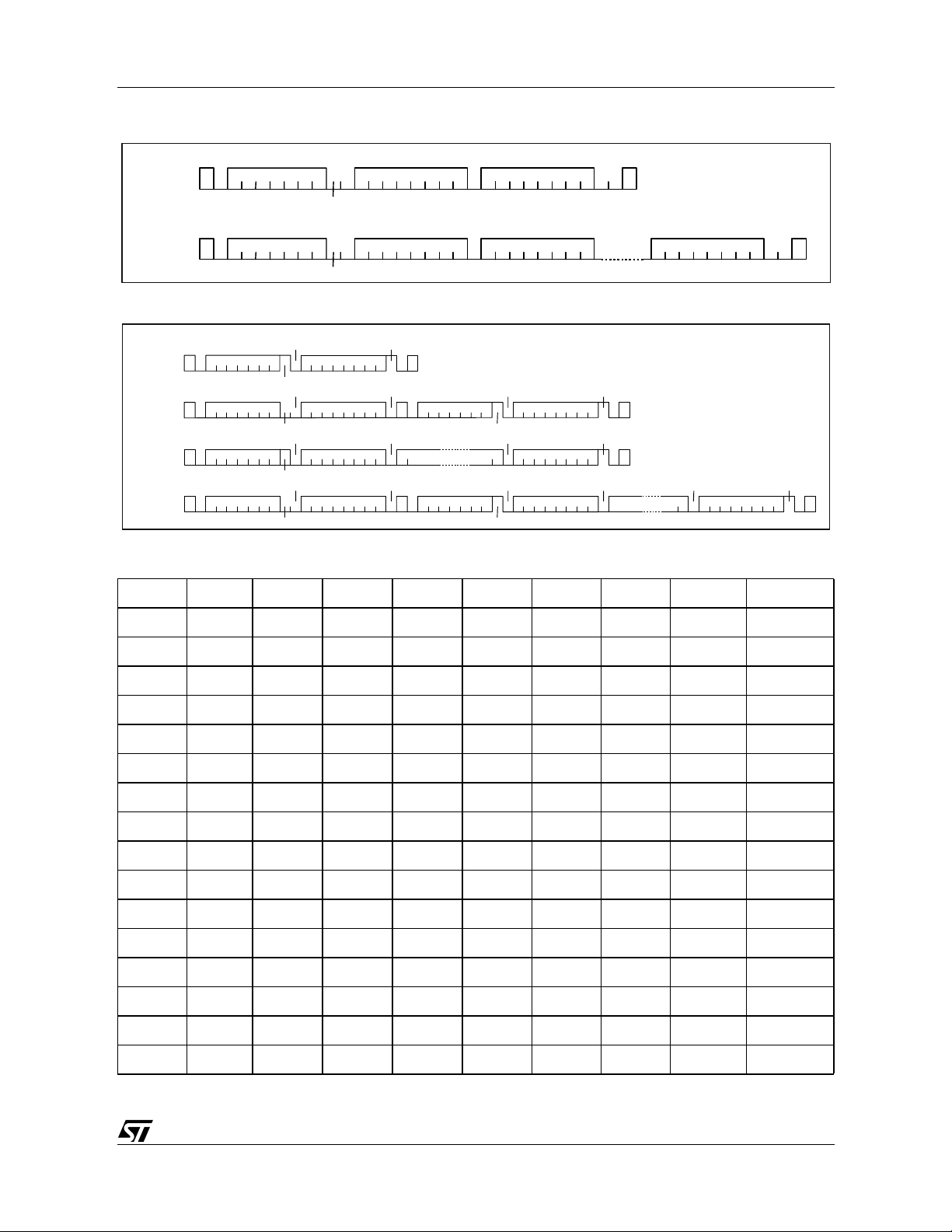
Write Mode Sequence
STA308
BYTE
WRITE
MULTIBYTE
WRITE
START
START
DEV-ADDR
DEV-ADDR
ACK
SUB-ADDR
RW
ACK
SUB-ADDR
RW
ACK
ACK
DATA IN
DATA IN
ACK
ACK
STOP
ACK
DATA IN
Read Mode Sequence
CURRENT
ADDRESS
READ
RANDOM
ADDRESS
READ
SEQUENTIAL
CURRENT
READ
SEQUENTIAL
RANDOM
READ
START
START
START
START
DEV-ADDR
DEV-ADDR
DEV-ADDR
DEV-ADDR
RW=
HIGH
ACK
RW
ACK
SUB-ADDR
RW
ACK
ACK
SUB-ADDR
RW
DATA
DATA
NO ACK
STOP
ACK
DEV-ADD R
START RW
ACK
DATA
ACK
DEV-ADD R
START RW
ACK
ACK
ACK
DATA
DATA
DATA
NO ACK
NO ACK
ACK
STOP
STOP
DATA
ACK NO ACK
DATA
Table 1. Register summary
Address Name D7 D6 D5 D4 D3 D2 D1 D0
STOP
STOP
00h ConfA MPC HPE BME IR1 IR0 MCS2 MCS1 MCS0
01h ConfB DRC ZCE SAI FB SAI2 SAI1 SAI0 ZDE DSPB
02h ConfC HPB CSZ4 CSZ3 CSZ2 CSZ1 CSZ0 OM1 OM0
03h ConfD B QL PSL COS1 COS0 C78BO C56BO C34BO C12BO
04h ConfE D CV SAOFB SAO2 SAO1 SAO0 DEMP VOLEN MIXE
05h C onfF EAPD AME COD I2SD PWMD
06h Mm ute MMute
07h Mvol MV7 MV6 MV 5 MV4 MV3 MV2 MV1 MV0
08h Cmute C8M C7M C6M C5M C4M C3M C2M C1M
09h C1Vol C1V7 C1V6 C1V5 C1V4 C1V3 C1V2 C1V1 C1V0
0Ah C2Vol C2V7 C2V6 C2V5 C2V4 C2V3 C2V2 C2V1 C2V0
0Bh C3Vol C3V7 C3V6 C3V5 C3V4 C3V3 C3V2 C3V1 C3V0
0Ch C4Vol C4V7 C4V6 C4V5 C4V4 C4V3 C4V2 C4V1 C4V0
0Dh C5Vol C5V7 C5V6 C5V5 C5V4 C5V3 C5V2 C5V1 C5V0
0Eh C6Vol C 6V7 C6V6 C6V5 C6V4 C6V3 C6V2 C6V1 C6V0
0Fh C7Vol C7V7 C7V6 C7V5 C7V4 C7V3 C7V2 C7V1 C7V0
9/33

STA308
10h C8Vol C8V7 C8V6 C8V5 C8V4 C8V3 C8V2 C8V1 C8V0
11h C1 2im C2IM2 C2IM1 C2IM0 C1IM2 C1IM1 C1IM0
12h C34im C4IM2 C4IM1 C4IM0 C3IM2 C3IM1 C3IM0
13h C56im C6IM2 C6IM1 C6IM0 C5IM2 C5IM1 C5IM0
14h C78im C8IM2 C8IM1 C8IM0 C7IM2 C7IM1 C7IM0
15h C1234ls C4LS1 C4LS0 C3LS1 C3LS0 C2LS1 C2LS0 C1LS1 C1LS0
16h C5678ls C8LS1 C8LS0 C7LS1 C7LS0 C6LS1 C6LS0 C5LS1 C5LS0
17h L1ar L1R3 L1R2 L1R1 L1R0 L1A3 L1A2 L1A1 L1A0
18h L1atrt L1AT3 L1AT2 L1AT1 L1AT0 L1RT3 L1RT2 L1RT1 L1RT0
19h L2ar L2R3 L2R2 L2R1 L2R0 L2A3 L2A2 L2A1 L2A0
1Ah L2atrt L2AT3 L2AT2 L2AT1 L2AT0 L2RT3 L2RT2 L2RT1 L2RT0
1Bh Tone TTC3 TTC2 TTC1 TTC0 B TC3 BTC2 BTC1 BTC0
1Ch Cfaddr CFA7 CFA6 CFA5 CFA4 CFA3 CFA2 CFA1 CFA0
1Dh B 2cf1 C1B23 C1B22 C1B21 C1B20 C1B19 C1B18 C1B17 C1B16
1Eh B2cf2 C1B15 C1B14 C1B 13 C1 B12 C1B11 C1B10 C1B9 C1B8
1Fh B2cf3 C1B7 C1B6 C1B5 C1B4 C1B3 C1B2 C1B1 C1B0
20h B0cf1 C 2B23 C2B2 2 C2B21 C2B20 C2B19 C2B18 C2B17 C2B16
21h B0cf2 C 2B15 C2B1 4 C2B13 C2B12 C2B11 C2B10 C2B9 C2B8
22h B0cf3 C2B7 C2B6 C2B5 C2B4 C2B3 C2 B2 C2B1 C2B0
23h A2cf1 C 3B23 C3B2 2 C3B21 C3B20 C3B19 C3B18 C3B17 C3B16
24h A2cf2 C 3B15 C3B1 4 C3B13 C3B12 C3B11 C3B10 C3B9 C3B8
25h A2cf3 C3B7 C3B6 C3B5 C3B4 C3B3 C3 B2 C3B1 C3B0
26h A1cf1 C 4B23 C4B2 2 C4B21 C4B20 C4B19 C4B18 C4B17 C4B16
27h A1cf2 C 4B15 C4B1 4 C4B13 C4B12 C4B11 C4B10 C4B9 C4B8
28h A1cf3 C4B7 C4B6 C4B5 C4B4 C4B3 C4 B2 C4B1 C4B0
29h B1cf1 C 5B23 C5B2 2 C5B21 C5B20 C5B19 C5B18 C5B17 C5B16
2Ah B 1cf2 C5B15 C5B14 C5B13 C5B12 C5B11 C5B10 C5B9 C5B8
2Bh B 1cf3 C5B7 C5B6 C5 B5 C5B4 C5B3 C5B2 C5B1 C5B0
2Ch Cfud WA W1
2Dh D C1 DCC23 DCC22 DCC21 DCC20 DCC19 DCC18 DCC 17 D CC16
2Eh DC2 D CC15 DCC14 DCC13 DCC12 DCC11 DCC 10 DCC9 DCC8
2Fh BI ST1 R4 BEND R3BEND R2BEND R1BEND R4BACT R3B ACT R2BACT R1BACT
30h BIST2 R5BBAD R4 BBAD R3B BAD R2BBAD R1BBAD
10/33
 Loading...