

STA304
DIGITAL AUDIO PROCESSOR WITH MULTICHANNEL DDX™
PRODUCT PREVIEW
■ END TO END DIGITAL AUDIO INTEGRATED
SOLUTION
■ · DSP Functions:
- DIGITAL VOLUME CONTROL
- SOFT MUTE
- BASS and TREBLE
- PARAMETRIC EQ PER CHANNEL
- BASS MANAGEMENT FOR SUBWOO FER
- AUTO MU TE ON ZERO IN P U T DETECTION
■ 4+1 DIRECT DIGITAL AMPLIFICATION
(DDX™) OUTPUT CHANNELs
■ 6 CHANNELs PROGRAMMABLE SERIAL
OUTPUT INTERFACE (by default I2S)
■ 4 CHANNELs PROGRAMMABLE SERIAL
INPUT INTERFACE (by default I2S)
■ STEREO S/PDIF INPUT INTERFACE
■ Intel AC'97 LINK (rev. 2. 1) INPUT INTERFACE
FOR AUDIO AND CONTROL
■ ON CHIP AUTOMATIC INPUT SAMPLING
FREQUENCY DETECTION
■ 100 dB SNR SAMPLE RATE CONVERTER
(1KHz SINUSOIDAL INPUT)
2
■ I
C CONTROL BUS
■ LOW POWER 3.3V CMOS TECHNOLOGY
ORDERING NUMBER: STA304
■ EMBEDDED PLL FOR INTERNAL CLOCK
GENERATION (1024x48 kHz = 49.152 MHz)
■ 24.576 MHz EXTERNAL INPUT CLOC K OR
BUILT-IN INDUSTRY STANDARD XTAL
OSCILLATOR.
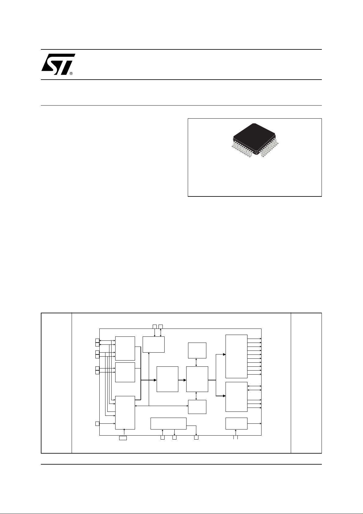
1.0 DESCRIPTION
The STA304 Digital Audio Processor is a single chip
device implementing end to end digital solution for
audio application. In conjunction with STA500 power
bridge it gives the full digital DSP-to-power high quality chain with no need for audio Digital-to- Analog converters between DSP and power stage.
TQFP44
BLOCK DIAGRAM
SCL SDA
10 9
LRCKI / SYNC
BICKI / BIT_CL
SDI_1 / SDATA_OUT
SDI_2/ SDATA_IN
January 2002
This is preliminary information on a new product foreseen to be developed. Details are subject to change without notice.
RESET
3
4
1
2
RXP
18
RXN
19
7
I2S
S/PDIF
AC`97
11
SA
I2C
PLL
14 15 43
XTI XTO
ROM
DSPSRC
RAM
CKOUT
DDX
I2S
PowerDown
44
PWDN
29
30
27
28
33
34
23
24
21
22
43
43
43
43
43
35
LEFT_B
LEFT_A
RIGHT_B
RIGHT_A
SLEFT_A
SLEFT_B
SRIGHT_A
SRIGHT_B
LFE_A
LFE_B
LRCKO
BICKO
SDO_1
SDO_2
SDO_3
EAPD
1/30
STA304
1.0 DESCRIPTION
(continued)
The device supports two main configurations as far as input sources: AC'97 input or IIS/SPDIF input: selection
is made via a dedicated pin (
AC97_MODE
pin). The AC`97 can be configured to work in two different ways:
'Full Compliant' mode and 'Proprietary' mode which enables more features. The selection of the operating mode
is done via a specific bit in a Vendor Reserved register (see bit 0: AC97_FC_mode in the CRA register, address
5Ah).
The 'Full Compliant' mode is compliant with rev. 2.1 of AC`97 link specifications.
This link can provide up to 6 input audio channels with sampling frequency of 44.1, 48, 88.2, 96 kHz, and the
related controls.
In the IIS/SPDIF mode, a ster eo S/P DIF and a 4 channels three- wires pr ogrammable serial input i nter face wor k
in mutually exclusive way. Two channels with sampling frequency in the continuous range from 32 to 96 kHz
are supported by the S/PDIF interface. Up to four channels with sampling frequency varying continuously from
32kHz up to 96 kHz are supported by the programmable serial interfaces. Among the different configurations,
also the standard IIS protocol is supported.
An embedded high quality sample rate convert er (SRC) resamples input data at the internal fix ed sampling frequency of 48 kHz for DSP operations.
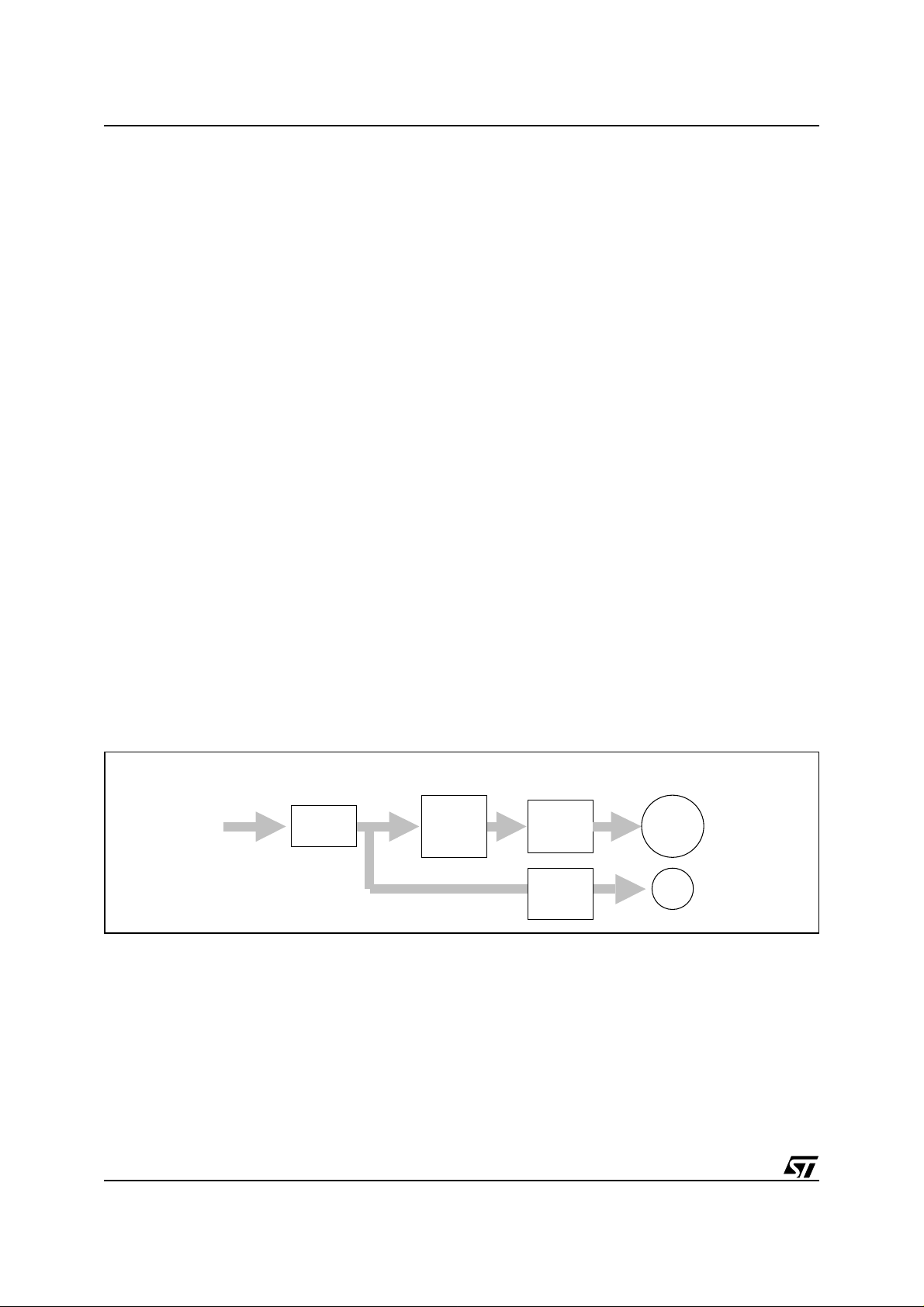
The DSP is a 20x20 bit core audio processor performing several user controlled parametric algorithms, among
them are dynamic and static equalization, Bass, Treble, Volume control and more. The DSP operates at
49.152MHz (1024xfs). This frequency is generated by an internal PLL with programmable multiplication factor
(x2 or x8).
This device has 5 channels Direct Digital Amplification (DDX™ technology), performing high efficiency class-D
PWM output signals used to drive directly external power bridge stages (STA500).
In addition a 6 channel digital output programmable interface (supporting IIS standard protocol) is embedded
for applications with commercial audio D/A converters. The output sampling frequency is fixed at 48 kHz when
the interface operates as master. In addition an oversampled clock (256xfs or 512xfs) is provided externally for
the D/A converters.
An IIC interface allows full programmability of internal algorithms and contro l registers via an external controller.
An arbitration logic handles access conflicts to e mbedded control registers (which may occur as a conse quence
of contemporary access to control registers by AClink, IIC and DSP blocks).
Figure 1. DSP data processing
L, R, SL,
SR, LFE,
CNT
Bass
Redir
2/30
L, R, SL,
SR, LFE
.
CNT
Static
&
Dinamic
EQ
Volume
Ctrl.
Center
Volume
Ctrl.
I2S
+
DDX
I2S

STA304
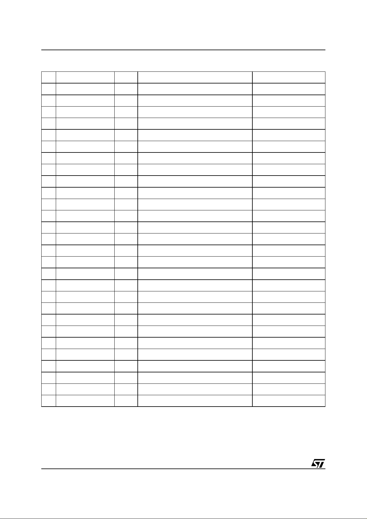
PIN CONNECTION
(Top view)
SDI_1/SDATA_OUT
SDI_2/SDATA_IN
LRCKI/SYNC
BICKI/BIT_CLK
AC97_MODE
VDD_1
GND_1
RESET
SDA
SCL
SA
SDO_1
SDO_2
SDO_3
SCKO
GND_5
VDD_5
CKOUT
PWDN
44 43 42 41 3940 38 37 36 35 34
1
2
3
4
5
6
7
8
9
10
12 13 14 15 16
VDD_2
TEST_MODE
XTI
XTO
GND_2
171118 19 20 21 22
RXP
VCC
RXN
EAPD
LRCKO
VSS
LFE_B
SLEFT_A
33
32
31
30
29
28
27
26
25
24
23
LFE_A
SLEFT_B
VDD_4
GND_4
LEFT_A
LEFT_B
RIGHT_A
RIGHT_B
VDD_3
GND_3
SRIGHT_A
SRIGHT_B
D00AU1160
PIN FUNCTION
PIN NAME TYPE DESCRIPTIO N PAD TYPE
1 SDI_1 / SDATA_OUT I Input I2S Serial Data 1 / AC97 Output Data CMOS Schmitt In
2 SDI_2 / SDATA_IN I/O Input I2S Serial Data 2 / AC97 Input Data CMOS In / CMOS Out 2mA
3 LRCKI / SYNC I/O Input I2S Left/Right Clock / AC97 Synch.
CMOS In / CMOS Out 2mA
Clock
4 BICKI / BIT_CLK I/O Input I2S Serial Clock / AC97 Bit Clock CMOS In / CMOS Out 4mA
5 VDD_1 Digital Supply Voltage
6 GND_1 Digital Ground
7 RESET I Global Reset
CMOS Schmitt In Pull-Up
(This pin is sensed only after 2 clock cycles)
8 AC97_MODE I AC97 Enable / Disable (1=AC97; 0=I2S/
CMOS Schmitt In Pull-Down
SPDIF)
9 SDA I/O I2C Serial Data CMOS In / CMOS Out 2mA
10 SCL I I2C Serial Clock CMOS In
11 SA AC97 Primary/Secondary Codec Selector CMOS In
12 TEST_MODE I Test Mode (Active High) CMOS
13 VDD_2 Digital Supply Voltage
14 XTI I Crystal Input (Clock input) Analog IN
15 XTO O Crystal Output CMOS Out Oscill. Pad
16 GND_2 Digital Ground
3/30
STA304
PIN FUNCTION
PIN NAME TYPE DESCRIPTIO N PAD TYPE
17 VCC Analog Supply Voltage
18 RXP I S/PDIF receiver positive Analog In
19 RXN I S/PDIF receiver negative Analog In
20 VSS Analog Ground
21 LFE_B O Pwm LFE (subwoofer) output channel (B) CMOS Out 3mA
22 LFE_A O Pwm LFE (subwoofer) output channel (A) CMOS Out 3mA
23 SRIGHT_B O Pwm Surround Right output channel (B) CMOS Out 3mA
24 SRIGHT_A O Pwm Surround Right output channel (A) CMOS Out 3mA
25 GND_3 Digital Ground
26 VDD_3 Digital Supply Voltage
27 RIGHT_B O Pwm Right output channel (B) CMOS Out 3mA
28 RIGHT_A O Pwm Right output channel (A) CMOS Out 3mA
29 LEFT_B O Pwm Left output channel (B) CMOS Out 3mA
30 LEFT_A O Pwm Left output channel (A) CMOS Out 3mA
(continued)
31 GND_4 Digital Ground
32 VDD_4 Digital Supply Voltage
33 SLEFT_B O Pwm Surround Left output channel (B) CMOS Out 3mA
34 SLEFT_A O Pwm Surround Left output channel (A) CMOS Out 3mA
35 EAPD O External Amplifier Powerdown (Active Low) CMOS Out 2mA
36 LRCKO I/O Output I2S Left/Right Clock CMOS In / CMOS Out 2mA
37 SDO_1 O Output I2S Serial Data 1 CMOS Out 2mA
38 SDO_2 O Output I2S Serial Data 2 CMOS Out 2mA
39 SDO_3 O Output I2S Serial Data 3 CMOS Out 2mA
40 SCKO I/O Output I2S Serial Clock CMOS In / CMOS Out 4mA
41 GND_5 Digital Ground
42 VDD_5 Digital Supply Voltage
43 CKOUT O Clock Output (12 /24 MHz) CMOS Out 8mA
44 PWDN I Device Powerdown (Active Low) CMOS In Pull-Up
4/30
STA304
ABSOLUTE MAXIMUM RATINGS
Symbol Parameter Value Unit
V
DD
V
V
T
stg
T
op
P
DD
P
DA
Power Supply -0.3 to 4 V
Voltage on input pins -0.3 to VDD+0.3 V
i
Voltage on output pins -0.3 to VDD+0.3 V
o
Storage Temperature -40 to +150 °C
Operative ambient temperature -20 to +85 °C
Power Consumption Digital tbd mW
Power Consumption Analog tbd mW
THERMAL DATA
Symbol Parameter Value Unit
R
thj-amb
Thermal resistance Junction to Ambient 85 °C/W
ELECTRICAL CHARACTERISTCS
(VDD from 2.9V up to 3.4V; T
= 0 to 70 °C; unless otherwise specified)
amb
DC OPERATING CONDITIONS
Symbol Parameter Value
V
DD
T
j
Power Supply Voltage 3.0 to 3.6V
Operating Junction Temperature -20 to 125 °C
GENERAL INTERFACE ELECTRICAL CHARACTERISTICS
Symbol Parameter Test Condition Min. Typ. Max. Unit Note
Low Level Input Current Without
I
il
pull-up device
I
High Level Input Current
ih
Without pull-up device
V
Note 1: The leakage currents are generally very small, < 1na. The value given here is a maximum that can occur after an electrostatic stress
Note 2: Human Body Model
Electrostatic Protection Leakage < 1µA2000 V2
esd
on the pin.
Vi = 0V -10 10 µA1
Vi = VDD = 3.6V -10 10 µA1
5/30
STA304
DC ELECTRICAL CHARACTERISTICS
Symbol Parameter Test Condition Min. Typ. Max. Unit Note
V
Low Level Input Voltage
il
0.2*V
DD
V
V
V
V
Note 1: Takes into account 200mV voltage drop in both supply lines
Note 2: X is the source/sinc current under worst case conditions and is reflected in the name of the I/O cell according to the drive capability.
I
R
T
T
Note 1: Mi n condition: Vdd = 3.0V, 125°C Min process; M ax. conditio n: Vdd = 3.6 V, -20°C m ax process.
DIGITAL CHARACTERISTICS-SPDIF RECEIVER (RXP,RXN pins only, SPDIF - MODE = ANALOG)
ZIN Input Resistance kΩ
VTH Dufferential Input Voltage
VHY Input Hysteresis 50 mV
High Level Input Voltage
ih
Low Level Output Voltage Iol = X mA
ol
High Level Output Voltage
oh
Pull-up current Vi = 0V;
pu
Equivalent Pull-up resistance 50 KΩ
pu
Reset Active Time 2·T
R
Master Clock Period ns
CK
V
DD
= 3.3V
0.8*V
DD
0.4*V
0.85*V
DD
-25 -66 -125 µA1
CK
1
----------------- -
49.152
200
DD
V
V 1,2
V 1,2
ns
mV
2.0 AC’97 BANK REGISTER OVERVIEW
The AC `97 interface is compliant t o ‘Aud io Codec ` 97 – Revision 2.1’ specifi cation, as far as the protocol used.
All the registers described in this specification, including Standard, Vendor Reserved and Extended Audio (AC
`97 2.0) registers, are available in this device, but just relevant registers which are described in paragraph 11
(Register Summary) are implemented.
The ATE mode feature has been implemented for test purpose: for related deta ils refer to the
– Revision 2.1
’ specification.
‘Audio Codec `97
2.1 Reading AC `97 Registers
Since the AC`97 register bank has been implemented as a contiguous RAM space (from a DSP point of view)
the content of the RAM itself will be returned as the result of a read operation. This should be followed as a
general rule of thumb but, where not possible, a different approach has been used. Hereby is a list of the registers, and bits, that do not follow this rule or that have a particular handling:
• CodecID_0, CodecID_1
:
These two bit are respectively bits 14 and 15 of registers 28h (Extended Audio ID) and 3Ch (EWxtended
Modem ID). When a read oper ation o f these registers is performed the retur ned value is based on the s tatus
of the SA pin: CodecID_0 report the status of SA pin, CodecID_1 always report 0. Other bits of these registers return the related RAM register contents. Also note that the status of the SA pin is not readable by the
DSP.
•PR4
:
The bit 12 of register 26h (Powerdown, ctrl/start) is used to set the AC`97 BIT_CLK and SDATA_IN signal
to a low state. In response to a Warmers the status of this bit is set back to its default 0 value. In response
6/30

STA304
to a read request the actual value of this signal is returned, not the R AM content. Due to this fact the relati ve
RAM register content can be incongruous.
• Regs
For more details regarding a specific bit please refer to the appropriate paragraph.
In order to be as much compliant to the specification as possible two different mode of operation has been in-
troduced. Using the
(default): in this mode the value returned as response to a read operation will be properly masked in order to
set ‘reserved’ bits to 0, as from specification. This operation is perform ed on all registers inclu ded the Standard
or Extended Audio address space. If the Full-Compliant mode is not selected the full 16 bits data from the corresponding RAM register will be returned with no further manipulation.
If an odd-addressed register reading operation is performed the following scheme is adopted:
• Slot 0: report valid bit set to 1 for both slot 1 and slot 2
• Slot 1 (address):report the odd address
• Slot 2 (data): report all 0s
. 2Ch, 2Eh and 30h (Audio Sample Rate Control):
These three registers are used to setup the sample rate when the Variable Rate Mode is enabled. In response to a read request on one of these registers the actual value returned can be either BB80h or AC44h,
depending on the s tatus of an internal har dware signal; the s tatus of this signal i s update d ever y time a wr ite
operation into one of these register is performed.
AC97_FC_Mode
configuration bit the interface can be configured in Full-Compliant mode
2.2 Writing AC `97 Registers
When a write operation into one of the available AC`97 registers is performed the entire 16 bits data word is
written into the related RAM register (also
have a corresponding
the value of the FF is also updated every time a write to the related RAM register is performed. The status of
these FF is reverted to their default values after a hardware rese t or a software reset (w riting to r eg. 00h) request
has been issued; as a consequence also the DSP will have to reset the RAM register contents.
Some register may have a different behaviour from the one depicted above. Here is a brief summary of those
registers.
hardware register ( Fli p-Flop)
reserved
bits are passed through). Some bits of some register may
, used to control the internal status of the device: in this c ase
• Regs. 7Ch and 7Eh:
These are the Vendor ID1 and ID2 registers. Any write request to one of these will be ignored.
• Regs. 28h:
The ‘
Extended Audio ID Register
’ is read only. Therefore any write request will be ignored.
• Regs. 26h:
When a write request is issued the actual data written into the RAM register is ‘xxxxxxxxxxxx1110’, where
‘x’ stands for the incoming data.
• Regs. 2Ah:
When a write request is issued the actual data written into the RAM register is ‘xxxxxx0111xxxxxx’, where
‘x’ stands for the incoming data.
• Regs. 32h and 34h:
Any write request into one of these
corresponding RAM register.
ADC sample rate register
will result in the value BB80h written into the
7/30
STA304
3.0 I2S INPUT INTERFACE CONFIGURATION
In order to configure the I2S input interface the
I2SI_Align_x bits one of 6 configuration mod e can be selected. Following is a table descr ibing each one o f them.
MODE # of SLOTS W. LENGHT ALIGNMENT DELAY SLOT NOTES
0 32 24 Left No
1 32 24 Left Yes
2 32 16 Right No MSb first only
3 32 24 Right No
4 24 24 Left No Slave only
5 Not valid Not valid Not valid Not valid Reserved, do not use.
6 24 16 Right No MSb first only. Slave only
7 24 24 Right No Slave only
Configuration Register B (CRB
) can be used. Using the 3
By default standard I2 S i nput interfac e slave is provided (mode 1 in bits 0,1,2 of regi ster CRB, I2S_BICK_Pol = 1
I2SI_LRCK_Pol = 0 with some register)
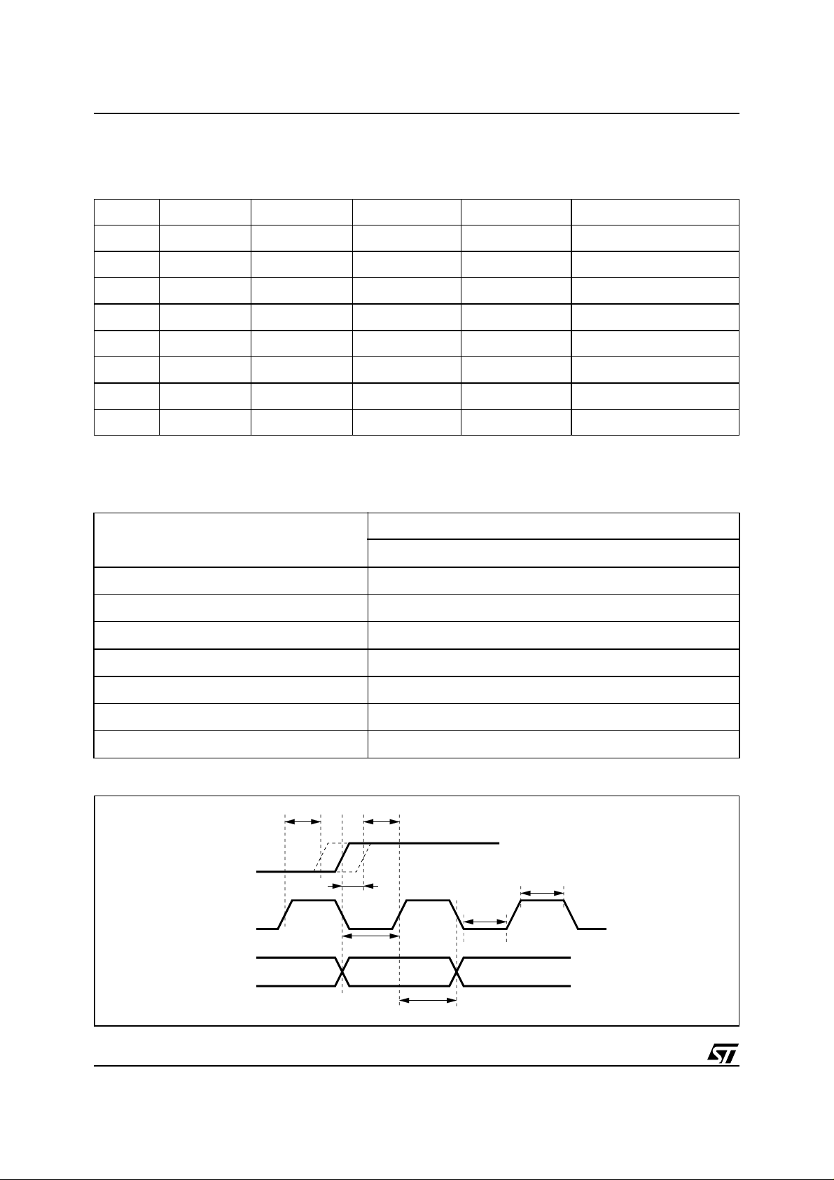
3.1 Switching characteristics (10 pf load; Fsm=32 KHz to 96KHz):
BICKI frequency (master mode):
(slave mode):
BICKI pulse width low (T
BICKI pulse width high (T
BICKI active to LRCKI edge delay (T
BICKI active to LRCKI edge setup (T
SDI valid to BICKI active setup (T
) (slave mode): min 40 ns.
0
) (slave mode): min 40 ns.
1
): min 20 ns.
2
): min 20 ns.
3
): min 20 ns.
4
BICKI active to SDI hold time (T5): min 20 ns.
BICKI falling to LRCKI edge (T
) (master mode): min 3 ns; max 9 ns.
6
3.072MHz
Max 6.4 MHz
Figure 2.
T
2
T
3
and
8/30
LRCKI
BICKI
SDI
T
T
6
T
0
T
4
T
5
1
D00AU1244
STA304
4.0 I2S OUTPUT INTERFACE CONFIGURATION
In order to configure the I2S output interface the
I2SO_Align_x bits one of 6 configuration mode can be selected. Following is a table describing each one of
them.
MODE # of SLOTS W. LENGHT ALIGNMENT DELAY SLOT NOTES
0 32 24 Left No
1 32 24 Left Yes
2 32 16 Right No MSb first only
3 32 24 Right No
4 24 24 Left No Slave only
5 Not valid Not valid Not valid Not valid Reserved, do not use.
6 24 16 Right No MSb first only. Slave only
7 24 24 Right No Slave only
By default standard I2S output interface master is provided (mode 1 in bits 8,9,10 of register CRB,
I2SO_BICK_Pol = 1 and I2SO_LRCK_Pol = 0 in the same register)
Configuration Register B (CRB
) can be used. Using the 3
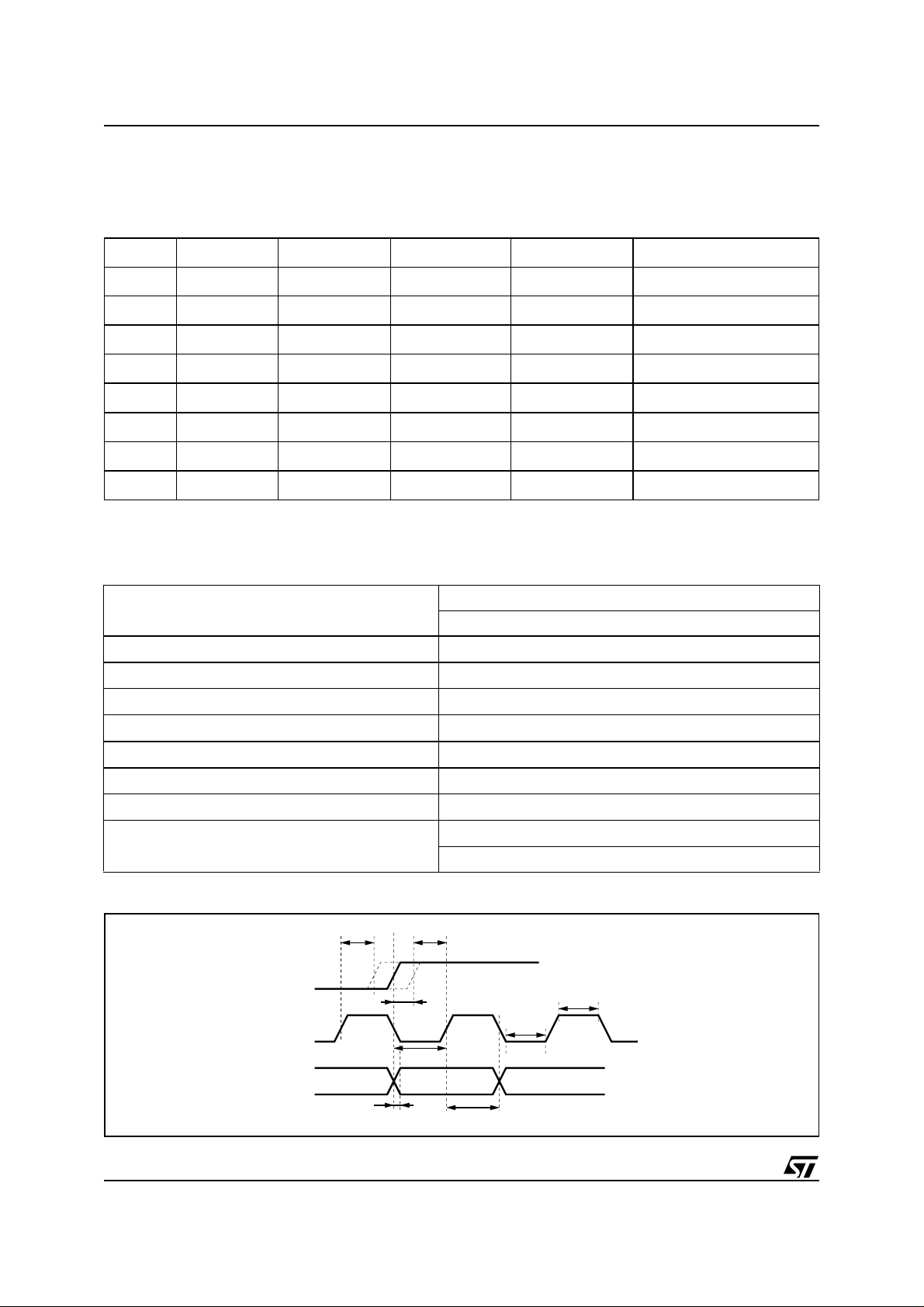
4.1 Switching characteri stics (10 pf load; Fsm=48 KHz):
SCKO frequency (master mode): 64 Fsm
(slave mode): 64 Fsm
SCKO pulse width low (T
SCKO pulse width high (T
SCKO active to LRCKO edge delay (T
SCKO active to LRCKO edge setup (T
SDO valid to SCKO active setup (T
SCKO active to SDO hold time (T
SCKO falling to LRCKO edge (T
SCKO falling to SDO edge(T
) (slave mode): min 40 ns.
0
) (slave mode): min 40 ns.
1
): min 20 ns.
2
): min 20 ns.
3
): min 20 ns.
4
): min 20 ns.
5
) (master mode): min 2 ns; max 8 ns.
6
) (master mode): min 2 ns; max 8 ns.
7
(slave mode): min 6 ns; max 17 ns
Figure 3.
LRCKO
BICKO
T
2
T
3
T
6
T
1
T
0
9/30
SDO
T
4
T
7
T
5
D00AU1245
 Loading...