

SGS Thomson Microelectronics STA020D, STA020 Datasheet

96kHz DIGITAL AUDIO INTERFACE TRANSMITTER
MONOLITHIC DIGITAL AUDIO INTERFACE
TRANSMITTER
3.3V SUPPLYVOLTAGE
SUPPORTS:
- AES/EBU,IEC 958,
- S/PDIF,& EIAJCP-340
- Professionaland Consumer Formats
PARITYBITSAND CRCCODESGENERATED
TRANSPARENT MODE ALLOWS DIRECT
CONNECTIONOF STA020 AND STA120
STA020
PRODUCT PREVIEW
SDIP24 SO24
DESCRIPTION
The STA020 is a monolithic CMOS device which
encodes and transmits audio data according to
the AES/EBU, IEC 958, S/PDIF, & EIAJ CP-340
interface standards. It supports 96kHz sample
rate operation
The STA020 accepts audio and digital data which
is then multiplexed, encoded and driven onto a
cable.
The audio serial port is double buffered and ca-
BLOCK DIAGRAM
VD+
7
SCK
FSYNC
SDATA
M0 M1 M2 MCK RST
212223
6
7
8
10
C
11
U
9
V
AUDIO
SERIAL PORT
REGISTERS
ORDERING NUMBERS:
STA020 STA020D
pable of supportinga wide variety of formats.
The STA020 multiplexes the channel, user, and
validity data directly from serial input pins with
dedicated input pins for the most important channel statusbits.
GND
19
18
MUX DIFFERENTIAL
165
20
17
TXP
TXN
15 24
DEDICATED CHANNEL
STATUS BUS
October 1999
This is preliminaryinformation on a new product now in development. Details are subjectto change without notice.
CBL TRNPT
D97AU599A
1/12
STA020
ABSOLUTE MAXIMUM RATINGS
Symbol Parameter Value Unit
V
D+
V
IND
T
amb
T
stg
RECOMMNDED OPERATINGCONDITIONS(GND = 0V; all voltageswith respect to ground)
Symbol Parameter Test Condition Min. Typ. Max. Unit
V
D+
T
amb
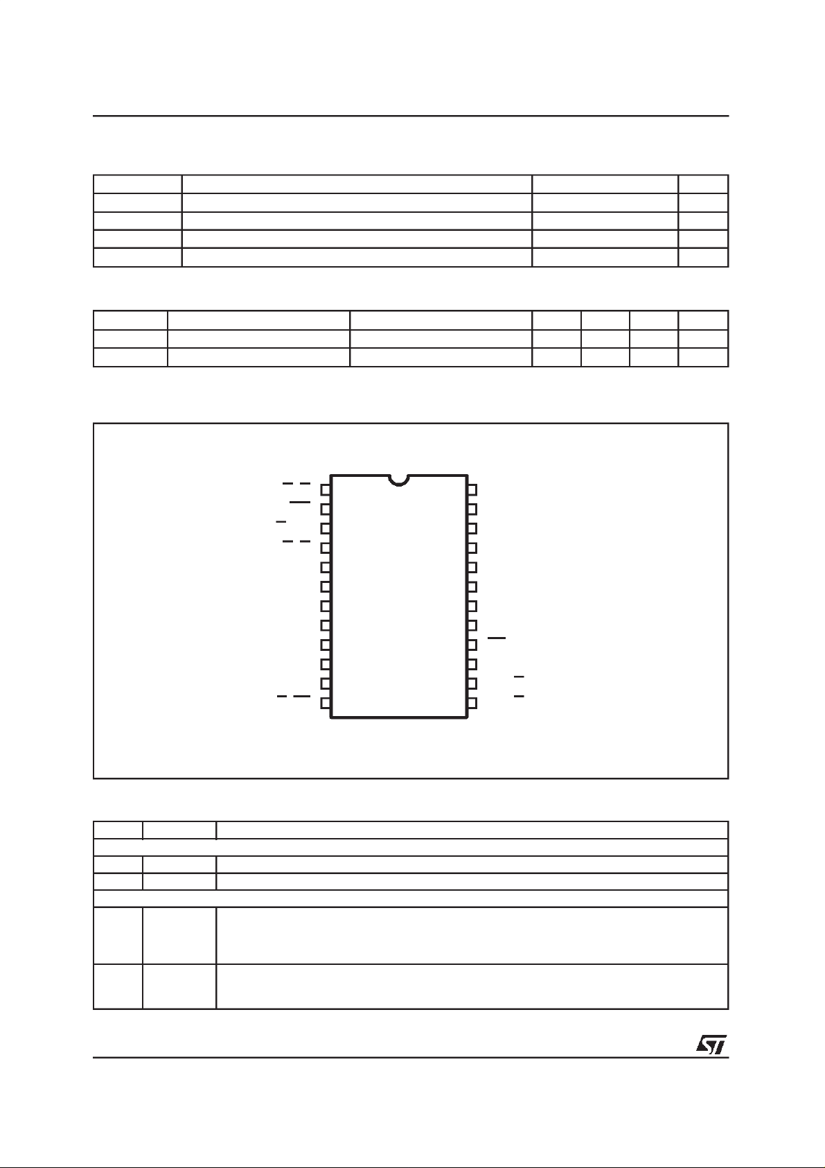
PIN CONNECTION
DC Power Supply 4 V
Digital Input Voltage -0.3 to VD+0.3 V
Ambient Operating Temperature (power applied) -20 to +85 °C
Storage Temperature -40 to 150 °C
DC Voltage 3 3.3 3.6 V
Ambient Operating Temp. 0 25 70 °C
C7/C3
PRO
C1/FC0
C6/C2
MCK TXP
SCK
FSYNC
SDATA
C/SBF
C9/C15
1
2
3
4
5
6
7
8
V
9
10
U
11
12
D97AU608A
24
23
22
21
20
18
17
16
15
14
13
PINS DESCRIPTION
N. Name Function
Power Supply Connections
18 GND Ground.
19 VD+ Positive Digital Power. Nominally +3.3V.
Audio Input Interface
6 SCK Serial Clock.
7 FSYNC Frame Sync.
Serial clock for SDATA pinwhich can be configured (via the M0, M1 and M2 pins) as an input
or output and can sample data on the rising or falling edge.As an output, SCK will contain 32
clocks for everyaudio sample.
Delineates the serial data andmay indicate the particular channel, left or right and may be an
input or output. The format is based on M0, M1 and M2 pins.
TRNPT/FC1
M0
M1
M2
VD+19
GND
TXN
RST
CBL/SBC
EM0/C9
EM1/C8
2/12

PINS DESCRIPTION(continued)
N. Name Function
8 SDATA Serial Data.
21,
22,23
Control Pins
Transmitter Interface
20, 17 TXP, TXN Differential Line Drivers.
M0, M1, M2 Serial Port Mode Select.
1 C7/C3 Channel Status Bit 7/Channel Status Bit 3.
2 PRO Professional/Consumer Select.
3 C1/FC0 Channel Status Bit 1/Frequency Control 0.
4 C6/C2 Channel Status Bit 6/Channel Status Bit 2.
9 V Validity.
10 C/SBF Channel Status Serial Input/Subcode Frame Clock.
11 U User Bit.
12 C9/C15 Channel Status Bit 9/ChannelStatus Bit 15.
13 EM1/C8 Emphasis 1/Channel Status Bit 8.
14 EM0/C9 Emphasis 0/Channel Status Bit 9.
15 CBL/SBC Channel Status Block Output/Subcode Bit Clock.
16 RST Master Reset.
24 TRNPT/FC1 Transparent Mode/Frequency Control 1.
5 MCK Master Clock. Clock input at 128xthe sample frequency which definesthe transmit timing. In
Audio data serial input pin.
Selects the format of FSYNC and the sample edge of SCK withrespect to SDATA.
In professional mode, C7 is the inverse of channel status bit 7. In consumer mode, C3 is the
inverse of channel status bit 3, C7/C3 are ignored in Transparent Mode.
Selects between professional mode (PRO low) and consumer mode(PRO high). This pin
defines the functionality of the channelstatus parallel pins. PRO is ignored in Transparent
Mode.
In professional mode, C1 is the inverse of channel status bit 1. Inconsumer mode, FC0and
FC1 are encoded versions of channel status bits 24 and 25 (bits 0 and 1 of byte 3). When
FC0 and FC1 are both high, CD mode is selected. C1/FC0 are ignored in Transparent Mode.
In professional mode, C6 is the inverse of channel status bit 6. Inconsumer mode, C2 is the
inverse of channel status bit 2. C6/C2 are ignored in Transparent Mode.
Validity bit serial input port. This bitis defined as per the digital audio standards wherein V = 0
signifies the audio signal is suitable for conversion to analog. V = 1 signifiesthe audio signal is
not suitable for conversion to analog,i.e. invalid.
In professional and consumer modes this pin is the channel status serial input port. In CD
mode this pin inputs theCD subcode frame clock.
User bit serial input port.
In professional mode, C9 is the inverse of channel status bit 9 (bit 1 of byte 1). In consumer
mode, C15 is the inverse of channel status bit 15 (bit7 of byte 1). C9/C15 are ignored in
Transparent Mode.
In professional mode, EM0 and EM1 encode channelstatus bits2, 3 and 4. Inconsumer
mode, C8 is the inverse of channel status bit 8 (bit 0 of byte 1). EM1/C8 are ignored in
Transparent Mode.
In professional mode, EM0 and EM1 encode channelstatus bits2, 3 and 4. Inconsumer
mode, C9 is the inverse of channel status bit 9 (bit 1 of byte 1). EM0/C9 are ignored in
Transparent Mode.
In professional and consumer modes, the channel status block output is high for the first 15
bytes of channel status. In CD mode, this pin outputs the subcode bitclock.
When low, all internal counters are reset.
In professional mode, setting TRNPT low selects normal operation & CBL is an output. Setting
TRNPT high, allows the STA020 to be connected directly to an STA120. In transparent mode,
CBL is an input& MCK must be at 256Fs. In consumer mode, FC0 and FC1 are encoded
versions of channel status bits 24 and 25. When FC0 and FC1 are both high, CD mode is
selected.
trasparent mode MCK must be 256 Fs.
STA020
3/12

STA020
DIGITAL CHARACTERISTICS (T
=25°C; VD+= 3.3V ±10%)
amb
Symbol Parameter Test Condition Min. Typ. Max. Unit
V
IH
V
IL
V
OH
V
OL
I
in
High-Level Input Voltage 2.0 VDD+0.3 V
Low-Level Input Voltage -0.3 +0.8 V
High-Level Output Voltage IO= 200µAV
-1.0 V
DD
Low-Level Output Voltage IO= 3.2mA 0.4 V
Input Leakage Current 1.0 10 µA
MCK Master Clock frequency (Note 1) 26 MHz
Master Clock Duty Cycle (high time/cycle time) 40 60 %
Note 1: MCKmust be 128x the input word rate, except in TransparentMode where MCK is 256x the inputword rate.
Figure 1. STA020 Professional& ConsumerModesTypical Connection Diagram.
AUDIO
DATA
PROCESSOR
µCONTROLLER
or
UNUSED
CHANNEL
STATUS BITS
CONTROL
FSYNC
SCK
SDATA
CBL
RST
EXTERNAL
CLOCK
MCK
5
7
6
8
15
C
10
U
V
STA020
11
9
16
8 DEDICATED C.S. BITS
+3.3V
19
VD+
18
24
23
22
21
20
17
GND
TRNPT
M0
M1
M2
TXP
TXN
0.1µF
SERIAL PORT
MODE SELECT
TRANSMITTER
CIRCUIT
D97AU600A
Figure 2. STA020 Typical ConnectionDiagram.
EXTERNAL
4/12
AUDIO
DATA
PROCESSOR
DECODER
SUBCODE
PORT
RESET
CONTROL
CHANNEL
STATUS BITS
CONTROL
FSYNC
SDATA
7
SCK
6
8
V
9
SBF
10
U
11
SBC
15
RST
16
8 DEDICATED C.S. BITS
CLOCK
5
STA020
MCK
+5V
19
VD+
0.1µF
GND
18
M0
23
M1
22
M2
21
TXP
20
TXN
17
SERIAL PORT
MODE SELECT
TRANSMITTER
CIRCUIT
See Appendix B
D99AU989A
 Loading...