

STA015 STA015B STA015T
MPEG 2.5 LAYER III AUDIO DECODER
SINGLE CHIP MPEG2 LAYER 3 DECODER
SUPPORTING:
- All features specifiedfor Layer III in ISO/IEC
11172-3(MPEG 1 Audio)
- All features specifiedfor Layer III in ISO/IEC
13818-3.2(MPEG2 Audio)
- Lowersamplingfrequenciessyntaxextension,
(not specifiedby ISO) called MPEG 2.5
DECODES LAYER III STEREO CHANNELS,
DUAL CHANNEL, SINGLE CHANNEL
(MONO)
SUPPORTING ALL THE MPEG 1 & 2 SAMPLING FREQUENCIES AND THE EXTENSIONTO MPEG 2.5:
48, 44.1, 32, 24, 22.05, 16, 12, 11. 025, 8 KHz
ACCEPTS MPEG 2.5 LAYER III ELEMENTARY COMPRESSED BITSTREAM WITH
DATARATE FROM 8 Kbit/sUP TO 320 Kbit/s
ADPCMCODECCAPABILITIES:
- samplefrequencyfrom 8 kHzto 32 kHz
-samplesizefrom8bitsto32bits
- encodi ngalgor i thm:DVI,
ITU- G726pack(G723- 24,G721,G723-40)
-Tonecontrolandfast-forwardcapability
EASY PROGRAMMABLE GPSO INTERFACE
FOR ENCODED DATA UP TO 5Mbit/s
(TQFP44&LFBGA 64)
DIGITALVOLUME
BASS& TREBLE CONTROL
SERIALBITSTREAM INPUT INTERFACE
EASY PROGRAMMABLE ADC INPUT INTER-
FACE
ANCILLARY DATA EXTRACTION VIA I2C IN-
TERFACE.
SERIAL PCM OUTPUT INTERFACE (I
ANDOTHER FORMATS)
PLL FOR INTERNAL CLOCK AND FOR OUT-
PUTPCM CLOCK GENERATION
CRC CHECK AND SYNCHRONISATION ER-
ROR DETECTION WITH SOFTWARE INDICATORS
2
I
C CONTROL BUS
LOW POWER2.4VCMOS TECHNOLOGY
WIDE RANGE OF EXTERNAL CRYSTALS
FREQUENCIES SUPPORTED
2
WITH ADPCM CAPABILITY
PRODUCT PREVIEW
ORDERING NUMBERS: STA015 (SO28)
APPLICATIONS
PC SOUNDCARDS
MULTIMEDIA PLAYERS
VOICERECORDERED
DESCRIPTION
The STA015 is a fully integrated high flexibility
MPEG Layer III Audio Decoder, capable of decoding Layer III compressedelementary streams,
as specified in MPEG 1 and MPEG 2 ISO standards. The device decodesalsoelementarystreams
S
compressedby usinglow samplingrates,as specifiedby MPEG2.5.
STA015 receives the input data through a Serial
Input Interface. The decoded signal is a stereo,
mono, or dual channel digital output that can be
sent directly to a D/Aconverter, by the PCM Output Interface.This interface is software programmable to adapt the STA015 digital output to the
most common DACs architectures used on the
market.
The functional STA015 chip partitioning is described in Fig.1 and Fig.2.
STA015T (TQFP44)
STA015B (LFBGA 64)
February 2000
This is preliminary informationon a new product now in development or undergoing evaluation. Details are subject to changewithout notice.
1/44

STA015-STA015B-STA015T
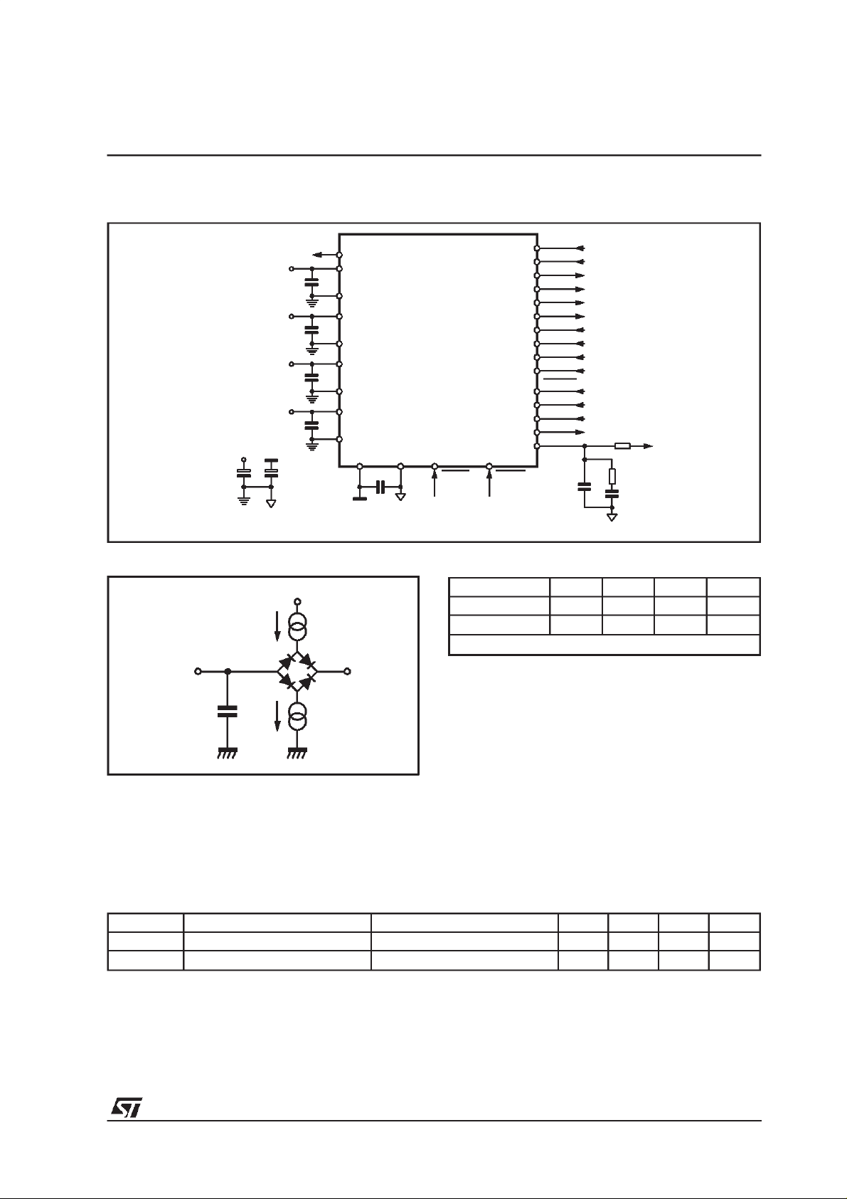
Figure1a. BLOCK DIAGRAM for TQFP44 and LFBGA64 package
SDA SCL
TQFP44
31 32
I2C CONTROL
34
SDI
SCKR
BIT_EN
DATA-REQ
SCK_ADC
CRCK_ADC
SDI_ADC
36
38
27
40
26
24
SERIAL
INPUT
INTERFACE
ADC
INPUT
INTERFACE
25
RESET
BUFFER
256 x 8
PARSER
SYSTEM & AUDIO CLOCKS
15 13 22 12
XTI XTO FILTTESTEN
MPEG L
ADPCM
CORE
Figure1b. BLOCK DIAGRAMfor SO28 package
SDA SCL
34
SO28
GPIO
INTERFACE
DSP BASED
42
III
VOLUME
& TONE
CONTROL
OUTPUT
BUFFER
PCM
OUTPUT
INTERFACE
GPSO
INTERFACE
D99AU1116
44
2
3
4
28
33
SDO
SCKT
LRCKT
OCLK
GPSO_REQ
GPSO_SCKL
GPSO_DATA
SDI
SCKR
BIT_EN
DATA-REQ
SCK_ADC
CRCK_ADC
SDI_ADC
2/44
5
6
7
28
8
27
25
SERIAL
INPUT
INTERFACE
ADC
INPUT
INTERFACE
BUFFER
256 x8
26
RESET
I2C CONTROL
MPEG L
PARSER
ADPCM
CORE
III
SYSTEM & AUDIO CLOCKS
21 20 24 19
XTI XTO FILTTESTEN
DSP BASED
VOLUME
&
TONE
CONTROL
OUTPUT
BUFFER
PCM
OUTPUT
INTERFACE
D99AU1117
9
SDO
10
SCKT
11
LRCKT
12
OCLK
Figure2. PINCONNECTIONS
STA015-STA015B-STA015T
VDD_1
VSS_1
SCKR
BIT_EN
SRC_INT/SCK_ADC
SCKT
LRCKT
OCLK
VSS_2
VDD_2
1
N.C.
2
LRCKT
3
OCLK
VSS_2
VDD_2
VSS_3
VDD_3
N.C.
PVDD
PVSS
4
5
6
7
8
9
10
GPSO_REQ
BIT_EN
IODATA[5]
28
27
26
25
24
23
22
21
20
19
18
17
16
1514
SCKR
IODATA[4]
1
2
3
SCL
SDI
SDO
44 43 42 41 3940 38 37 36 35 34
SCKT
SDO
IODATA[7]
4
5
6
7
SO28
8
9
10
11
12
13
D99AU1061
SRC_INT/SCK_ADC
IODATA[6]
TQFP44
XTI
IODATA[3]
IODATA[2]
171118 19 20 21 22
N.C.
VSS_4
IODATA[1]
IODATA[0]
12 13 14 15 16
FILT
XTO
OUT_CLK/DATA_REQ
LRCK_ADC
RESETSDA
SDI_ADC
TESTEN
VDD_4
VSS_4
XTI
XTO
FILT
PVSS
PVDD
VDD_3
VSS_3
SDI
GPIO/STROBE
33
GPSO_DATA
32
SCL
31
SDA
30
VSS_1
29
VDD_1
28
GPSO_SCKR
27
OUT_CLK/DATA_REC
26
LRCK_ADC
25
RESET
24
SDI_ADC
23
N.C.
D99AU1062
VDD_4
TESTEN
12345678
A1 =
SDI
A
B
C
D
E
F
G
H
B2 = SCKR
D4 = BIT_EN
D1 =
SRC_INT
E2 =
SDO
F2 = SCKT
H1 =
LRCKT
H3 =
OCLK
F3 =
VSS_2
E4 =
VDD_2
G4 =
VSS_3
G5 =
VDD_3
F5 = PVDD
G6 = PVSS
D00AU1149
G7 = FILT
G8 = XTO
F7 = XTI
E7 =
VSS_4
C8 =
VDD_4
D7 = TESTEN
A7 =
SDI_ADC
B6 = RESET
A5 =
LRCK_ADC
C5 =
OUT_CLK/DATA_REQ
B5 =
VDD_1
B4 =
VSS_1
A4 = SDA
B3 = SCL
C2 =
GPIO_STROBE
C3 = IODATA
E3 = IODATA
D2 = IODATA
F1 = IODATA
G3 =
GPSO_REQ
F8 = IODATA
F6 = IODATA
E6 = IODATA
C7 = IODATA
C6 =
GPSO_SCKR
[4]
[5]
[6]
[7]
[3]
[2]
[1]
[0]
A2 = GPSO_DATA
LFBGA64
3/44
STA015-STA015B-STA015T
1. OVERVIEW
1.1 - MP3 decoderengine
The MP3 decoder engine is able to decode any
Layer III compliant bitstream: MPEG1, MPEG2
and MPEG2.5 streams are supported. Besides
audio data decoding the MP3 engine also performs ANCILLARY data extraction: these data
can be retrieved via I2C bus by the application
microcontroller in order to implement specific
functions.
Decodedaudio data goesthrough a software volume control and a two-band equalizer blocks before feeding the output I2S interface. This results
in no need for an external audio processor.
MP3 bitstream is sent to the decoderusing a simple serial input interface (see pins SDI, SCKR,
BIT_EN and DATA_REQ), supporting input rate
up to 20 Mbit/s. Received data are stored in a
256 bytes long input buffer which provides a
ABSOLUTE MAXIMUM RATINGS
feedback line (see DATA_REQ pin) to the bitstreamsource (tipicallyan MCU).
1.2 - ADPCMencoder/decoder engine
This device also embeds a multistandardADPCM
encoder/decoder supporting different sample
rates (from 8 KHz up to 32 KHz) and different
sample sizes (from 8 bit to 32 bits). During encoding process two different interfaces can be
used to feeddata: theserial input interface (same
interface used also to feed MP3 bitstream) or the
ADC input interface, which provides a seamless
connection with an external A/D converter. The
currentlyused interface is selected via I2Cbus.
Also to retrieve encoded data two different interfaces are available: the I2C bus or the faster
GPSOoutput interface. GPSO interface is able to
output data with a bitrate up to 5 Mbit/s and its
control pins (GPSO_SCKR, GPSO_DATA and
GPSO_REQ)can be configuredin order to easily
fit thetarget application.
Symbol Parameter Value Unit
V
DD
V
i
V
O
T
stg
T
oper
Power Supply -0.3 to 4 V
Voltageon Input pins -0.3 to VDD+0.3 V
Voltageon output pins -0.3 to VDD+0.3 V
Storage Temperature -40 to +150 °C
Operative ambient temp -20 to +85 °C
THERMALDATA
Symbol Parameter Value Unit
R
th j-amb
Thermal resistance Junction to Ambient 85 °C/W
4/44
STA015-STA015B-STA015T
PIN DESCRIPTION
SO28 TQFP44 LFBGA64 Pin Name Type Function PAD Description
1 29 B5 VDD_1 Supply Voltage
2 30 B4 VSS_1 Ground
3 31 A4 SDA I/O i
4 32 B3 SCL I I
5 34 A1 SDI I Receiver Serial Data CMOS Input Pad Buffer
6 36 B2 SCKR I ReceiverSerial Clock CMOS Input Pad Buffer
7 38 D4 BIT_EN I Bit Enable CMOSInput Pad Bufferwith
8 40 D1 SRC_INT/SCK_ADC I Interrupt Line/ADC Serial
9 42 E2 SDO O TransmitterSerialData(PCMData) CMOS 4mA Output Drive
10 44 F2 SCKT O Transmitter Serial Clock CMOS 4mA Output Drive
11 2 H1 LRCLKT O Transmitter Left/Right Clock CMOS 4mA Output Drive
12 3 H3 OCLK I/O Oversampling Clock for DAC CMOS Input Pad Buffer
13 5 F3 VSS_2 Ground
14 6 E4 VDD_2 Supply Voltage
15 7 G4 VSS_3 Ground
16 8 G5 VDD_3 Supply Voltage
17 10 F5 PVDD PLL Power
18 11 G6 PVSS PLL Ground
19 12 G7 FILT O PLL Filter Ext. Capacitor
20 13 G8 XTO O Crystal Output CMOS 4mA Output Drive
21 15 F7 XTI I Crystal Input (Clock Input) Specific Level InputPad
22 19 E7 VSS_4 Ground
23 21 C8 VDD_4 Supply Voltage
24 22 D7 TESTEN I Test Enable CMOSInputPad Bufferwith
25 24 A7 SDI_ADC I ADC Data Input CMOS Input Pad Buffer
26 25 B6 RESET I System Reset CMOSInputPad Bufferwith
27 26 A5 LRCK_ADC I ADC Left/Right Clock CMOS Output Pad Buffer
28 27 C5 OUT_CLK/
DATA_REQ
20 C7 IODATA[0] I/O GPIO Data Line CMOS 4mA Schmitt Trigger
18 E6 IODATA[1] I/O GPIO DataLine
16 F6 IODATA[2] I/O GPIO Data Line
14 F8 IODATA[3] I/O GPIO Data Line
37 C3 IODATA[4] I/O GPIO Data Line
39 E3 IODATA[5] I/O GPIO DataLine
41 D2 IODATA[6] I/O GPIO Data Line
43 F1 IODATA[7] I/O GPIO Data Line
35 C2 GPIO_STROBE I/O GPIO Strobe Signal
4 G3 GPSO_REQ O GPSO Request Signal CMOS Output Pad Buffer
28 C6 GPSO_SCKR I GPSO Serial Clock CMOS Input Pad Buffer
33 A2 GPSO_DATA O GPSO Serial Data CMOS Output Pad Buffer
Note: In functional mode TESTEN must be connectedto VDD.
2
C Serial Data +
Acknowledge
2
C Serial Clock CMOS Input Pad Buffer
CMOS Input Pad Buffer
CMOS 4mA Output Drive
pullup
CMOS Input Pad Buffer
Clock
CMOS 4mA Output Drive
Conn.
(see paragraph 2.1)
pull up
pull up
O Buffered Output Clock/
CMOS 4mA Output Drive
Data Request Signal
Bidir Pad Buffer
5/44

STA015-STA015B-STA015T
1. ELECTRICAL CHARACTERISTICS:VDD = 3.3V ±0.3V;Tamb = 0 to 70°C;Rg = 50Ω unless otherwise
specified
DC OPERATINGCONDITIONS
Symbol Parameter Value
V
T
GENERAL INTERFACE ELECTRICAL CHARACTERISTICS
Symbol Parameter Test Condition Min. Typ. Max. Unit Note
Note 1: Theleakage currentsare generally very small, < 1nA. The valuegiven here is a maximum that can occur after an electrostaticstress
on the pin.
Note 2: Human Body Model.
DC ELECTRICALCHARACTERISTICS
Symbol Parameter Test Condition Min. Typ. Max. Unit Note
Power Supply Voltage 2.4to 3.6V
DD
Operating Junction Temperature -20 to 125°C
j
I
IL
Low LevelInput Current
Vi= 0V -10 10 µA1
Without pull-up device
I
IH
High Level Input Current
Vi=V
DD
-10 10 µA1
Without pull-up device
V
esd
V
IL
V
IH
V
ol
V
oh
Electrostatic Protection Leakage < 1µA 2000 V 2
Low LevelInput Voltage 0.2*V
High Level Input Voltage 0.8*VDD V
Low LevelOutput Voltage Iol= Xma 0.4V V 1, 2
High Level Output Voltage 0.85*V
DD
V
DD
V1,2
Note 1:
Takes into account 200mV voltage drop in both supplylines.
Note 2: Xis the source/sink current under worst case conditions and is reflected in thename of the I/O cell according to the drive capability.
Symbol Parameter Test Condition Min. Typ. Max. Unit Note
I
pu
R
pu
Pull-up current Vi= 0V; pinnumbers 7, 24
Equivalent Pull-up
and 26
-25 -66 -125 µA1
50 kΩ
Resistance
Note 1:
Min.condition: V
Max. condition: V
DD
= 2.7V, 125°C Min process
DD = 3.6V, -20°C Max.
POWERDISSIPATION
Symbol Parameter Test Condition Min. Typ. Max. Unit Note
PD Power Dissipation
@V
=3V
DD
Sampling_freq ≤24 kHz 76 mW
Sampling_freq ≤32 kHz 79 mW
Sampling_freq ≤48 kHz 85 mW
6/44
STA015-STA015B-STA015T
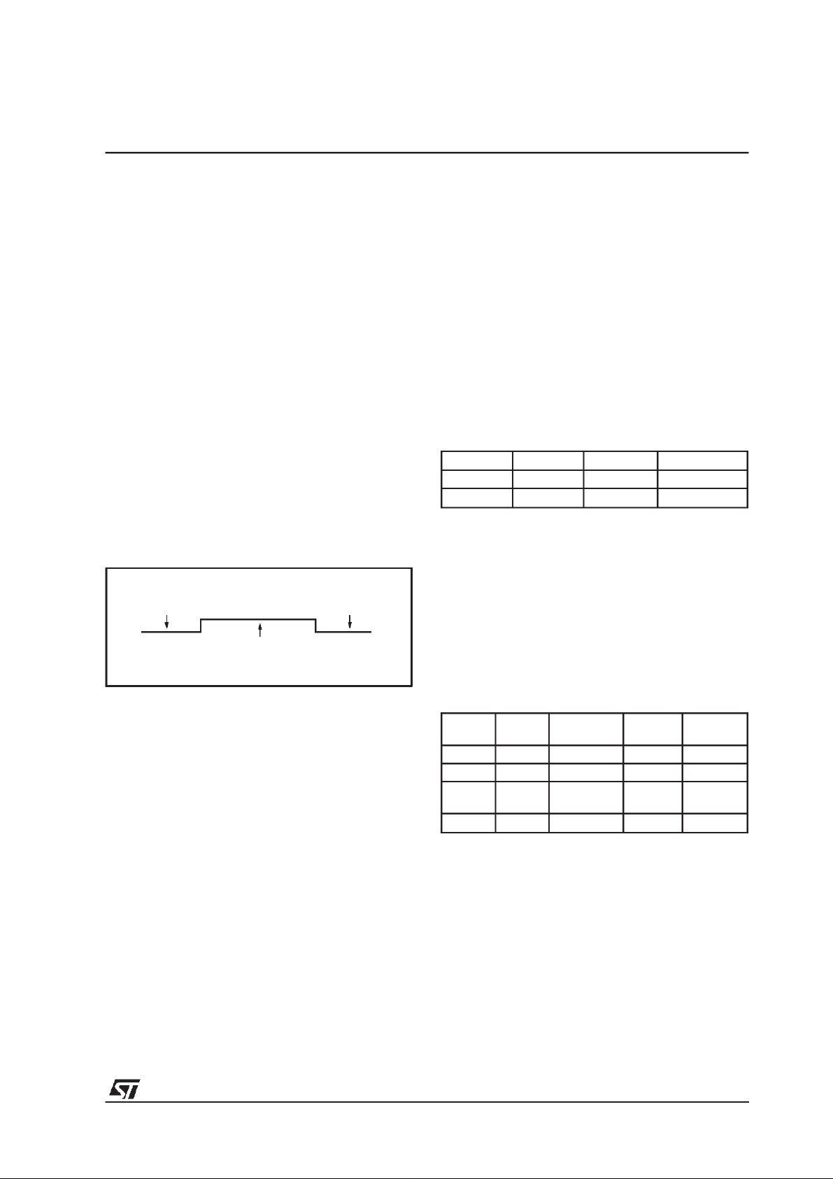
Figure3.
Test Circuit (refer to SO28 package)
OUT_CLK/DATA_REQ
PV
V
DD
PV
V
SS
Figure4. Test Load Circuit
I
OL
V
V
V
V
DD
SS
DD
100nF
DD
100nF
DD
100nF
DD
100nF
SDA
3
SCL
24
TESTEN
D00AU1143
4
9
10
11
12
5
6
7
25
8
27
21
20
19
SDO
SCKT
LRCKT
OCLK
SDI
SCKR
BIT_EN
SDI_ADC
SCR_INT
LRCK_ADC
XTI
XTO
470pF
10K
1K
4.7nF
PV
SS
1
V
SS
V
SS
V
SS
V
SS
2
14
13
16
15
23
22
17 182826
100nF4.7µF 4.7µF
PV
PV
SS
DD
RESET
Test Load
V
Output I
DD
SDA 1mA 100pF 3.6V
OL
Other Outputs 100µA 100µA 100pF 1.5V
I
OH
C
V
L
REF
OUTPUT
C
I
L
OH
2. FUNCTIONAL DESCRIPTION
2.1 - Clock Signal
The STA015 input clock is derivated from an external source or from a industry standard crystal
oscillator, generating input frequencies of 10,
V
REF
D98AU967
Other frequencies may be supported upon request to STMicroelectronics. Each frequency is
supported by downloading a specific configuration file, provided by STM
XTI is an input Pad with specificlevels.
14.31818 or14.7456 MHz.
Symbol Parameter Test Condition Min. Typ. Max. Unit
V
IL
V
IH
Low LevelInput Voltage VDD-1.8 V
High Level Input Voltage VDD-0.8 V
CMOScompatibility
The XTI pad low and high levels are CMOS compatible; XTI pad noise margin is better than typical
CMOSpads.
TTL compatibility
The XTI pad low level is compatible with TTL while the high level is not compatible(for example if V
DD =
3V TTL min high level = 2.0V while XTI min high level = 2.2V)
7/44

STA015-STA015B-STA015T
Figure5. PLL and Clocks GenerationSystem
XTI
N
PFD CP
M
FRAC
Update FRAC
Switching
Circuit
2.4 - PCM Output Interface
The decodedaudio data are output in serial PCM
format.The interface consists of the followingsignals:
SDO PCM Serial Data Output
SCKT PCM SerialClock Output
LRCLK Left/RightChannel SelectionClock
The output samples precision is selectable from
Figure6. PCM OutputFormats
16 SCLK Cycles
LRCKT
16 SCLK Cycles
R
CC
VCO
Disable PLL
OCLK
X
XTI2OCLK
DCLK
S
XTI2DSPCLK
16 to 24 bits/word, by setting the outputprecision
with PCMCONF (16, 18, 20 and 24 bits mode)
register. Data can be output either with the most
significant bit first (MS) or least significant bit first
(LS), selected by writing into a flag of the
PCMCONFregister.
Figure 8 gives a description of the several
STA015PCM OutputFormats.
The sample rates set decoded by STA015 is described in Table 1.
16SCLK Cycles
16 SCLK Cycles
16 SCLK Cycles
Table 1:
SDO
SDO
LRCKT
SDO
SDO
SDO
SDO
M
S
L
S
32 SCLK Cycles
M
L
S
S
M
0
S
L
M
0
S
S
M
S
M
L
S
S
L
M
S
S
32 SCLK Cycles
M
S
L
S
M
00
00
S
L
MSBMSB
S
L
M
S
S
L
M
S
S
32SCLK Cycles
L
S
M
S
M
S
MSL
00
L
S
L
S
L
S
S
M
00
S
MSL
S
MSL
MSB MSB
M
L
S
S
M
L
S
S
32 SCLK Cycles
M
0
L
S
00
S
L
S
S
M
0
S
L
M
0
S
S
M
S
PCM_ORD = 0
L
S
PCM_PRECis 16 bit mode
PCM_ORD = 1
M
S
PCM_PRECis 16 bit mode
32 SCLK Cycles
PCM_FORMAT = 1
0
PCM_DIFF = 1
PCM_FORMAT = 0
L
S
PCM_DIFF = 0
PCM_FORMAT = 0
PCM_DIFF = 1
PCM_FORMAT = 1
L
S
PCM_DIFF = 1
MPEGSampling Rates (KHz)
MPEG 1 MPEG 2 MPEG 2.5
48 24 12
44.1 22.05 11.025
32 16 8
8/44
STA015-STA015B-STA015T
2.5 - STA015Operation Mode
The STA015 can work in two different modes,
calledMultimediaMode and BroadcastMode.
In
Multimedia Mode
(default mode) STA015 decodes the incoming bitstream, acting as a master
of the data communication from the source to itself.
This control is done by a specific buffer management,controlledbySTA015 embedded software.
The data source, by monitoring the DATA_REQ
line, send to STA015 the input data, when the
signalis high (defaultconfiguration).
The communication is stopped when the
DATA_REQline is low.
In this mode the fractional part of the PLL is disabled and the audio clocks are generated at
nominal rates. Fig. 7 describes the default
DATA_REQ signal behaviour. Programming
STA015 it is possible to invert the polarity of the
DATA_REQline (register REQ_POL).
Figure7.
SOURCE STOPS TRANSMITTING DATA SOURCE STOPS TRANSMITTING DATA
DATA_REQ
SOURCE SEND DATA TO STA015
D00AU1144
In Broadcast Mode, STA015 works receiving a
bitstream with the input speed regulated by the
source. In this configuration the source has to
guarantee that the bitrate is equivalent to the
nominalbitrateof the decodedstream.
To compensate the difference between the nominal and the real sampling rates, the STA015 embedded software controls the fractional PLL operation. Portable or Mobile applications need
normally to operate in Broadcast Mode. In both
modes the MPEG Synchronisation is automatic
and transparentto the user.
2.6 - STA015Decoding States
There are three different decoder states: Idle,
Init, and Decode. Commands to change the de-
coding states are described in the STA015 I
2
C
registersdescription.
Idle Mode
In this mode the decoder is waiting for the RUN
command. This mode shouldbe used to initialise
the configuration registers of the device. The
DAC connected to STA015 can be initialised during this mode (set MUTE to 1).
PLAY MUTE Clock State PCM Output
X 0 Not Running 0
X 1 Running 0
Init Mode
”PLAY” and ”MUTE” changes are ignored in this
mode. The internal state of the decoder will be
updatedonly when the decoder changes from the
state ”init” to the state ”decode”.The ”init” phase
ends when the first decoded samples are at the
output stage of the device.
Decode Mode
This mode is completely described by the follow-
ing table:
PLAY MUTE Clock State
0 0 Not Running 0 No
0 1 Running 0 No
1 0 Running Decoded
1 1 Running 0 Yes
PCM
Output
Samples
Decoding
Yes
9/44

STA015-STA015B-STA015T
Figure8.
MPEGDecoder Interfaces.
DATA_REQ
SDI
DATA
SOURCE
D98AU912
SCKR
BIT_EN
Figure9. Serial Input Interface Clocks
SDI
XTO
XTI FILT
PLL
MPEG
DECODER
SERIAL AUDIO INTERFACE
RX TX
µP
IIC
SCL SDA
IIC
DATA IGNORED
SDO
SCKT
LRCKT
DAC
OCLK
SCKR
SCKR
BIT_EN
D98AU968A
2.2 - SerialInput Interface
STA015 receives the input data (MSB first)
thought the Serial Input Interface (Fig.5). It is a
serial communication interface connected to the
SDI (Serial Data Input) and SCKR (Receiver Serial Clock).
The interface can be configured to receive data
sampled on both rising and falling edge of the
SCKR clock. The BIT_EN pin, when set to low,
forces the bitstream input interface to ignore the
incoming data. For proper operation Bit_E
N line
should be toggled only when SCRK is stable low
(for both SCLK_POL configuration) The possible
configurationsare describedin Fig. 9.
2.3 - PLL & Clock Generator System
When STA015 receives the input clock, as described in Section 2.1, and a valid layer III input
bitstream, the internal PLL locks, providing to the
DSP Core the master clock (DCLK), and to the
SCLK_POL=0
SCLK_POL=4
DATA IGNOREDDATA VALID
Audio Output Interface the nominal frequenciesof
the incomingcompressedbit stream. The STA015
PLLblockdiagramisdescribedin Figure5.
The audio sample rates are obtained dividing the
oversampl i ng clock(OCLK)by softwareprogramm able factors. The operation is done by STA015 embeddedsoftwar eand it istrans parenttotheuser.
TheSTA015PLLcandrivedirectlymost of thecommercial DACs families, providing an over sampling
clock, OCLK, obtaineddividing the VCO frequency
witha softwareprogrammabledividers.
2.4 - GPSOOutput Interface
In order to retrieveADPCM encoded data a General Purpose Serial Output interface is available
(in TQFP44 and LFBGA64 packages only). The
maximum frequency for clock is the
GPSO_SCKR DSP system clock frequency divided by 3 (i.e. 8.192 MHz @ 24.58MHz).The interface is based on a simple and configurable 3lines protocol, as described by figure10.
10/44
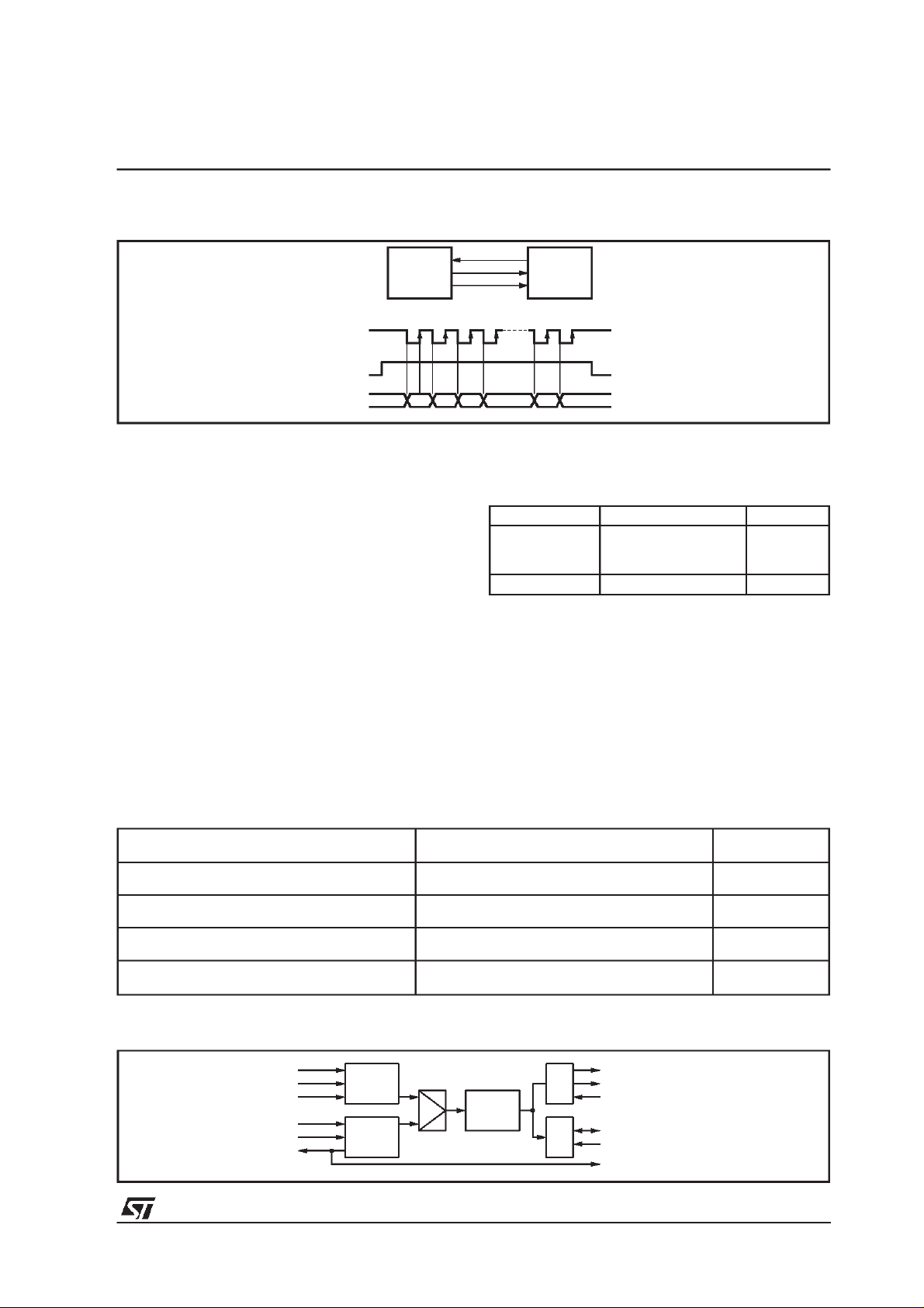
Figure10.
GPSO_SCKR
GPSO_REQ
GPSO_SCKR
STA015 MCU
GPSO_DATA
GPSO_REQ
STA015-STA015B-STA015T
GPSO_DATA
To enable the GPSO interface bit GEN of
GPSO_ENABLE register must be set. Using the
GPSO_CONFregister the protocol can be configured in order to provide outcoming data on ris-
ADPCM to provide an interrupt; the use of the
other bits is still to be defined. The related configurationregisteris GPIO_CONF.Seethe following summary for related pin usage:
D00AU1145
ing/falling edge of GPSO_SCKR input clock; the
GPSO_REQ request signal polarity (usually connected to an MCU interrupt line) can be configuredas well.
ADC Inteface
Name Description Dir
I/ODATA [0]
GPIO data line I/O
....................
I/ODATA [7]
GPIO_STROBE GPIO strobe line I/O
Beside the serial input interface based on SDI
and SCKR lines a 3 wire flexible and user configurable input interface is also available, suitable to
interface with most A/D converters. To configure
this interface 4 specificI
2
C registersare available
(ADC_ENABLE, ADC_CONF, ADC_WLEN and
ADC_WPOS). Refer to registers description for
more details.
2.5 ADPCM Encoding: Overview
According to the previously described interfaces
there are 4 ways to manage ADPCM data stream
while encoding. Input interface can be either the
serial receiver block (SDI + SCKR + DATA_REQ
lines) or the ADC specific interface.
Output interfaces can be either the I
General PurposeI/O Interface
A new general purpose I/O interface has been
added to this device (TQFP44 and LFBGA64
only). Actually only the strobe line is used in
INPUT (data to encode) Output (encoded data)
ADC I/F (SDI_ADC + LRCK_ADC + SCK_ADC) GPSO I/F (GPSO_REQ + GPSO_DATA +
ADC I/F (SDI_ADC + LRCK_ADC + SCK_ADC) I
SERIAL I/F (SCKR+ SDI + DATA_REQ) GPSO I/F (GPSO_REQ + GPSO_DATA +
SERIAL I/F (SCKR+ SDI + DATA_REQ) (*) I
(*) STA013 Compatible mode
GPSO_SCKR)
2
C + Interrupt (SCL + SDA + DATA_REQ) SO28/TQFP44
GPSO_SCKR)
2
C (polling) (SCL + SDA) SO28/TQFP44
or without interrupt line) or the GPSO high-speed
serial interface (GPSO_REQ + GPSO_ DATA +
GPSO_SCKRlines). This result in the following 4
methodsto handle encoding flow:
Figure.11
....
I/O
2
C bus (with
Available on
package
TQFP44
LFBGA64
LFBGA64
TQFP44
LFBGA64
LFBGA64
LRCK_ADC
SDI_ADC
SCK_ADC
SDI
SCKR
DATA_REQ
ADC I/F
SERIAL
RECEIVER
ENCOD
ENGINE
GPSOMUX
I2C
D99AU1064
GPSO_REQ
GPSO_DATA
GPSO_SCKR
SDA
SCL
DATA_REQ
11/44
STA015-STA015B-STA015T
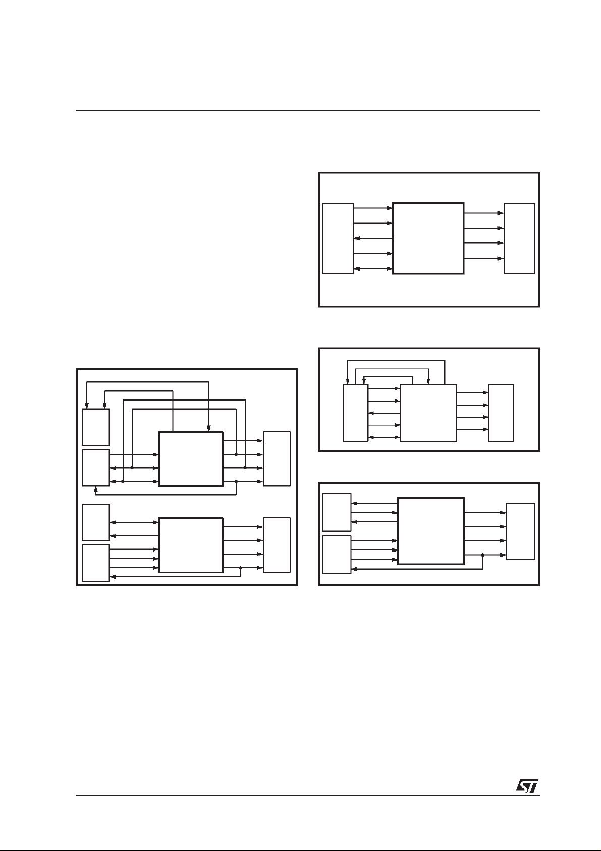
The following 4 figures (fig. 12, 13, 14, 15) show
the available connection diagrams as for as
ADPCM encoding function. As shown in the figures some configuration is not available in SO28
package.
Figure13. Input fromADC, Output from I2C +
IRQ
2
I
C
DATA_REQ
MCU
SDI_ADC
ADC
SLAVE
LRCKT
SCKT
STA015
SO28
TQFP44
LFBGA64
SDO
DAC
OCLK
Figure 12. Input from BITSTREAM,Outputfrom
I2C
SDI
SCKR
DATA_REQ
MCU DAC
BIT_EN
2
C
I
Figure 14.
Input from BITSTREAM,Outputfrom
STA015
SO28
TQFP44
LFBGA64
LRCKT
SCKT
SDO
OCLK
D99AU1121A
GPSO
GPSO_DATA
GPSO_SCKR
GPSO_REQ
MCU DACSTA015
Figure 15.
SDI
SCKR
DATA_REQ
BIT_EN
I2C
TQFP44
LFBGA64
Input from ADC, Output from GPSO
LRCKT
SCKT
SDO
OCLK
D99AU1122A
2
I
MCU
ADC
MASTER
C
DATA_REQ
LRCK_ADC
SCK_ADC
SDI_ADC
STA015
SO28
TQFP44
LFBGA64
LRCKT
SCKT
SDO
OCLK
DAC
D99AU1123A
3-I2C BUS SPECIFICATION
2
The STA015 supports the I
C protocol. This protocoldefines any device that sends data on to the
bus as a transmitter and any device that reads
the data as a receiver. The device that controls
the data transfer is known as the master and the
others as the slave. The master always starts the
transfer and provides the serial clock for synchronisation. The STA015 is always a slave device in
all its communications.
12/44
GPSO_DATA
MCU
ADC
MASTER
GPSO_SCKR
GPSO_REQ
LRCK_ADC
SCK_ADC
SDI_ADC
STA015
TQFP44
LFBGA64
LRCKT
SCKT
SDO
OCLK
DAC
D99AU1124A
3. 1 - COMMUNICATION PROTOCOL
3.1.0 - Datatransition or change
Data changes on the SDA line must only occur
when the SCL clock is low. SDA transition while
the clock is high are used to identify START or
STOP condition.
3.1.1 - Start condition
START is identified by a high to low transition of
the data bus SDA signal while the clock signal
SCL is stable in the high state.
A START condition must precede any command
fordata transfer.

STA015-STA015B-STA015T
3.1.2 - Stopcondition
STOP is identified by low to high transition of the
data bus SDA signal while the clocksignal SCL is
stable in the high state. A STOP condition terminates communications between STA015 and the
busmaster.
3.1.3 - Acknowledgebit
An acknowledgebit is used to indicate a successful data transfer. The bus transmitter, either master or slave, releases the SDA bus after sending
8 bit of data.
During the 9th clock pulse the receiver pulls the
SDA bus low to acknowledge the receipt of 8 bits
of data.
3.1.4 - Datainput
During the data input the STA015 samples the
SDA signalon the rising edgeof the clock SCL.
For correct device operation the SDA signal has
to be stable during the rising edge of the clock
and the data can changeonly when the SCL line
is low.
3.2 - DEVICEADDRESSING
To start communication between the master and
the STA015, the master must initiate with a start
condition. Following this, the master sends onto
the SDA line 8 bits (MSB first) corresponding to
the device select address and read or write
mode.
Figure16. Write Mode Sequence
The 7 most significant bits are the deviceaddress
identifier, corresponding to the I
2
C bus definition.
For the STA015 these are fixed as 1000011.
The 8th bit (LSB) is the read or write operation
RW, this bit is set to 1 in read mode and 0 for
write mode. After a START condition the STA015
identifies on the bus the device address and, if a
match is found, it acknowledges the identification
on SDA bus duringthe 9th bit time. The following
byte after the device identification byte is the internalspace address.
3.3 - WRITE OPERATION(see fig. 16)
Following a START condition the master sends a
deviceselectcode with the RW bit set to 0.
The STA015 acknowledges this and waits for the
byte of internaladdress.
After receiving the internal bytes address the
STA015againrespondswith an acknowledge.
3.3.1 - Bytewrite
In thebyte write mode the master sends one data
byte, this is acknowledged by STA015. The master then terminates the transfer by generating a
STOP condition.
3.3.2 - Multibytewrite
The multibyte write mode can start from any internal address. The transfer is terminated by the
mastergenerating a STOPcondition.
BYTE
WRITE
MULTIBYTE
WRITE
START
START RW
DEV-ADDR
DEV-ADDR
Figure17. Read Mode Sequence
ACK
CURRENT
ADDRESS
READ
RANDOM
ADDRESS
READ
SEQUENTIAL
CURRENT
READ
SEQUENTIAL
RANDOM
READ
DEV-ADDR
START
DEV-ADDR
START RW
START
START RW
DEV-ADDR
DEV-ADDR
RW=
HIGH
DATA
RW
ACK
SUB-ADDR
ACK
DATA
ACK
SUB-ADDR
ACK
RW
ACK
NO ACK
ACK
START RW
ACK
ACK
START RW
SUB-ADDR
SUB-ADDR
STOP
DATA
DEV-ADDR
DEV-ADDR
ACK
ACK
ACK
ACK
ACK
DATA IN
DATA IN
DATA
DATA
DATA
ACK
ACK
STOP
NO ACK
NO ACK
ACK
D98AU825B
STOP
STOP
DATA
DATA IN
ACK
ACK NO ACK
D98AU826A
STOP
DATA
STOP
13/44

STA015-STA015B-STA015T
3.4 - READOPERATION (see Fig. 17)
3.4.1 - Currentbyte address read
The STA015 has an internal byte address
counter. Each time a byte is written or read, this
counteris incremented.
For the current byte address read mode, following a START condition the master sends the deviceaddresswith the RW bit set to 1.
The STA015 acknowledges this and outputs the
byte addressed by the internal byte address
counter. The master does not acknowledge the
received byte, but terminates the transfer with a
STOPcondition.
3.4.2 - Sequential address read
This mode can be initiated with either a current
address read or a random address read. However in this case the master does acknowledge
the data byteoutputand the STA015 continues to
outputthe nextbyte in sequence.
To terminate the streams of bytes the master
does not acknowledge the last received byte, but
2
I
C REGISTERS
terminatesthe transfer with a STOP condition.
The output data stream is from consecutive byte
addresses,with the internal byte address counter
automaticallyincrementedafter one byte output.
2
C REGISTERS
4- I
The following table gives a description of the
MPEGSource Decoder (STA015)register list.
The first column (HEX_COD) is the hexadecimal
code for the sub-address.
The second column (DEC_COD) is the decimal
code.
The third column (DESCRIPTION) is the description of theinformationcontainedin the register.
The fourth column (RESET) inidicate the reset
value if any. When no reset value is specifyed,
the defaultis ”undefined”.
The fifth column (R/W) is the flag to distinguish
register ”read only” and ”read and write”, and the
useful size of the register itself.
Each register is 8 bit wide. The master shall operate reading or writing on 8 bits only.
HEX_COD DEC_COD DESCRIPTION RESET R/W
$00 0 VERSION R (8)
$01 1 IDENT 0xAC R (8)
$05 5 PLLCTL [7:0] 0xA1 R/W (8)
$06 6 PLLCTL [20:16] (MF[4:0]=M) 0x0C R/W (8)
$07 7 PLLCTL [15:12] (IDF[3:0]=N) 0x00 R/W (8)
$0C 12 REQ_POL 0x01 R/W (8)
$0D 13 SCLK_POL 0x04 R/W (8)
$0F 15 ERROR_CODE 0x00 R (8)
$10 16 SOFT_RESET 0x00 W (8)
$13 19 PLAY 0x01 R/W(8)
$14 20 MUTE 0x00 R/W(8)
$16 22 CMD_INTERRUPT 0x00 R/W(8)
$18 24 DATA_REQ_ENABLE 0x00 R/W(8)
$40 - $51 64 - 81 ADPCM_DATA_1 to ADPCM_DATA_18 0x00 R/W (8)
$40 64 SYNCSTATUS 0x00 R (8)
$41 65 ANCCOUNT_L 0x00 R (8)
$42 66 ANCCOUNT_H 0x00 R (8)
$43 67 HEAD_H[23:16] 0x00 R(8)
$44 68 HEAD_M[15:8] 0x00 R(8)
$45 69 HEAD_L[7:0] 0x00 R(8)
$46 70 DLA 0x00 R/W (8)
$47 71 DLB 0xFF R/W (8)
$48 72 DRA 0x00 R/W (8)
14/44

STA015-STA015B-STA015T
I2C REGISTERS(continued)
HEX_COD DEC_COD DESCRIPTION RESET R/W
$49 73 DRB 0xFF R/W (8)
$4D 77 CHIP_MODE 0x00 R/W (2)
$4E 78 CRCR 0x00 R/W (1)
$50 80 MFSDF_441 0x00 R/W (8)
$51 81 PLLFRAC_441_L 0x00 R/W (8)
$52 82 ADPCM_DATA_READY 0x00 R/W (1)
$52 82 PLLFRAC_441_H 0x00 R/W (8)
$53 83 ADPCM_SAMPLE_FREQ 0x00 R/W (4)
$54 84 PCM DIVIDER 0x03 R/W (8)
$55 85 PCMCONF 0x21 R/W (8)
$56 86 PCMCROSS 0x00 R/W (8)
$61 97 MFSDF (X) 0x07 R/W (8)
$63 99 DAC_CLK_MODE 0x00 R/W (8)
$64 100 PLLFRAC_L 0x46 R/W (8)
$65 101 PLLFRAC_H 0x5B R/W (8)
$67 103 FRAME_CNT_L 0x00 R (8)
$68 104 FRAME_CNT_M 0x00 R (8)
$69 105 FRAME_CNT_H 0x00 R (8)
$6A 106 AVERAGE_BITRATE 0x00 R (8)
$71 113 SOFTVERSION R (8)
$72 114 RUN 0x00 R/W (8)
$77 119 TREBLE_FREQUENCY_LOW 0x00 R/W (8)
$78 120 TREBLE_FREQUENCY_HIGH 0x00 R/W (8)
$79 121 BASS_FREQUENCY_LOW 0x00 R/W (8)
$7A 122 BASS_FREQUENCY_HIGH 0x00 R/W (8)
$7B 123 TREBLE_ENHANCE 0x00 R/W (8)
$7C 124 BASS_ENHANCE 0x00 R/W (8)
$7D 125 TONE_ATTEN 0x00 R/W (8)
$7E - B5 126 - 181 ANC_DATA_1 to ANC_DATA_56 0x00 R (8)
$B6 182 ISR 0x00 R/W (1)
$B8 184 ADPCM_CONFIG 0x00 R/W (2)
$B9 185 GPSO_ENABLE 0x00 R/W (1)
$BA 186 GPSO_CONF 0x00 R/W (2)
$BB 187 ADC_ENABLE 0x00 R/W (1)
$BC 188 ADC_CONF 0x00 R/W (5)
$BD 189 ADPCM_FRAME_SIZE 0x00 R/W (8)
$BE 190 ADPCM_INT_CFG 0x00 R/W (8)
$BF 191 GPIO_CONF 0x00 R/W (2)
$C0 192 ADC_ WLEN 0x0F R/W (5)
$C1 193 ADC_ WPOS 0x00 R/W (5)
$C2 194 ADPCM_SKIP_FRAME 0x00 R/W (8)
Note:
1) The HEX_COD is the hexadecimal adress thatthe microcontroller has to generate to access the information.
2) RESERVED: register used for production test only, or for future use.
15/44

STA015-STA015B-STA015T
4.1 - STA015REGISTERSDESCRIPTION
The STA015 device includes 256 I
2
C registers. In
this document, only the user-oriented registers
are described. The undocumented registers are
reserved. These registers must never be accessed (in Read or in Write mode). The ReadOnly registersmustneverbe written.
The following table describes the meaning of the
abbreviations used in the I
2
C registers descrip-
tion:
Symbol Comment
NA Not Applicable
UND Undefined
NC No Charge
RO Read Only
WO Write Only
R/W Read and Write
R/WS Read, Write in specific mode
VERSION
Address:0x00 (00)
Type:RO
MSB LSB
b7 b6 b5 b4 b3 b2 b1 b0
V8 V7 V6 V5 V4 V3 V2 V1
The VERSION register is read-only and it is used
to identify the IC on the applicationboard.
PLLCTL
Address:0x05 (05)
Type:R/W
SoftwareReset: 0xA1
HardwareReset: 0xA1
MSB LSB
b7 b6 b5 b4 b3 b2 b1 b0
XTO_
XTODISOCLKENSYS2O
BUF
PPLDISXTI2DS
CLK
PCLK
XTI2O
CLK
UPD_F
RAC
UPD_FRAC: when is set to 1, update FRAC in
the switching circuit. It isset to 1 after autoboot.
XTI2OCLK:when is set to 1, use the XTI as input
of the divider X instead of VCO output. It is set to
0 on HW reset.
XTI2DSPCLK:when is to 1, set use the XTI as input of the divider S instead of VCO output. It is
set to 0 onHW reset.
PLLDIS: when set to 1, the VCO output is disabled. It is set to 0 onHW reset.
SYS2OCLK: when is set to 1, the OCLK frequency is equal to the system frequency. It is
useful for testing. It is set to 0 on HW reset.
OCLKEN: when is set to 1, the OCLK pad is enable as outputpad. It is set to 1 on HW reset.
XTODIS: when is set to 1, the XTO pad is disable. It is set to0 on HW reset.
XTO_BUF: when this bit is set, the pin nr. 28
(OUT_CLOCK/DATA_REQ) is enabled. It is set
to 0 after autoboot.
IDENT
Address:0x01 (01)
Type:RO
SoftwareReset: 0xAC
HardwareReset: 0xAC
MSB LSB
b7 b6 b5 b4 b3 b2 b1 b0
10101100
IDENT is a read-onlyregister and is used to identify the IC onan applicationboard. IDENT always
hasthe value ”0xAC”
16/44
PLLCTL (M)
Address:0x06 (06)
Type:R/W
SoftwareReset: 0x0C
HardwareReset: 0x0C
PLLCTL (N)
Address:0x07 (07)
Type:R/W
SoftwareReset: 0x00
HardwareReset: 0x00
The M and N registers are used to configure the
STA015PLL by DSP embeddedsoftware.
M and N registers are R/W type but they are
completely controlled, on STA015, by DSP software.

STA015-STA015B-STA015T
REQ_POL
Address:0x0C (12)
Type:R/W
SoftwareReset: 0x01
HardwareReset: 0x00
The REQ_POL registers is used to program the
polarityof the DATA_REQ line.
MSB LSB
b7 b6 b5 b4 b3 b2 b1 b0
00000001
Default polarity (the source sends data when the
DATA_REQline is high)
MSB LSB
b7 b6 b5 b4 b3 b2 b1 b0
00000101
Invertedpolarity (the source sends data when the
DATA_REQline is low)
SCKL_POL
Address:0x0D (13)
Type:R/W
SoftwareReset: 0x04
HardwareReset: 0x04
MSB LSB
b7 b6 b5 b4 b3 b2 b1 b0
XXXXX000(1)
100(2)
X = don’t care
SCKL_POL is used to select the working polarity
of the Input Serial Clock (SCKR).
(1) If SCKL_POL is set to 0x00, the data (SDI)
are sent with thefalling edge of SCKR
and sampled on the risingedge.
(2) If SCKL_POL is set to 0x04, the data (SDI)
are sent with therising edge of SCKRand
sampledon the falling edge.
ERROR_CODE
Address:0x0F (15)
Type:RO
SoftwareReset: 0x00
HardwareReset: 0x00
MSB LSB
b7 b6 b5 b4 b3 b2 b1 b0
X X EC5 EC4 EC3 EC2 EC1 EC0
X = don’t care
ERROR_CODE register contains the last error
occourredif any. The codes can be as follows:
Code Description
0x00 No error since the last SW or HW Reset
0x01 CRC Failure
0x02 DATA not available
0x04 Ancillary data not read
0x10 Audio synch word not found
0x2X MPEG Header error
0x3X MPEG Decoding errors
SOFT_RESET
Address:0x10 (16)
Type:WO
SoftwareReset: 0x00
HardwareReset: 0x00
MSB LSB
b7 b6 b5 b4 b3 b2 b1 b0
XXXXXXX0
1
X = don’t care; 0 = normal operation; 1 = reset
When this registeris written, a soft reset occours.
The STA015 core command register and the interrupt register are cleared. The decoder goes in
to idle mode.
PLAY
Address:0x13 (19)
Type:R/W
SoftwareReset: 0x01
HardwareReset: 0x01
MSB LSB
b7 b6 b5 b4 b3 b2 b1 b0
XXXXXXX0
1
X = don’t care; 0 = normal operation; 1 = play
The PLAY command is handled according to the
state of the decoder,as described in section 2.5.
PLAY only becomes active when the decoder is
in DECODE mode.
17/44

STA015-STA015B-STA015T
MUTE
Address:0x14 (20)
Type:R/W
SoftwareReset: 0x00
HardwareReset: 0x00
MSB LSB
b7 b6 b5 b4 b3 b2 b1 b0
XXXXXXX0
1
X = don’t care; 0 = normaloperation; 1 = mute
The MUTE command is handled according to the
stateof the decoder,as described in section 2.5.
MUTEsetsthe clock running.
DATA_REQ_ENABLE
Address:0x18 (24)
Type:R/W
SoftwareReset: 0x00
HardwareReset: 0x00
CMD_INTERRUPT
Address:0x16 (22)
Type:R/W
SoftwareReset: 0x00
HardwareReset: 0x00
MSB LSB
b7 b6 b5 b4 b3 b2 b1 b0
XXXXXXX0
1
X = don’t care;
0 = normaloperation;
1 = write into I
2
C/AncillaryData
The INTERRUPT is used to give STA015 the
command to write into the I2C/Ancillary Data
Buffer (Registers: 0x7E ... 0xB5). Every time the
Master has to extract the new buffer content it
writes into this register, setting it to a non-zero
value.
MSB LSB
b7 b6 b5 b4 b3 b2 b1 b0 Description
X X X X X 0 X X buffered output clock
X X X X X 1 X X request signal
The DATA_REQ_ENABLE register is used to
configure Pin n. 28 working as buffered output
clock or data request signal, used for multimedia
mode.
The buffered Output Clock has the same fre-
quencythan the input clock (XTI)
SYNCSTATUS
Address:0x40 (64)
Type:RO
SoftwareReset: 0x00
HardwareReset: 0x00
MSB LSB
b7 b6 b5 b4 b3 b2 b1 b0 Description
XXXXXXSS1SS0
0 0 Research of sync word
0 1 Wait for Confirmation
1 0 Synchronised
18/44

STA015-STA015B-STA015T
ADPCM_DATA BUFFER
Address:0x40 - 0x51 (64 - 81)
Type:R/W
SoftwareReset: 0x00
HardwareReset: 0x00
MSB LSB
b7 b6 b5 b4 b3 b2 b1 b0
ENCODED DATA N to N+18
ANCCOUNT_L
Address:0x41 (65)
Type:RO
SoftwareReset: 0x00
HardwareReset: 0x00
MSB LSB
b7 b6 b5 b4 b3 b2 b1 b0
AC7 AC6 AC5 AC4 AC3 AC2 AC1 AC0
ANCCOUNT_H
Address:0x42 (66)
Type:RO
SoftwareReset: 0x00
HardwareReset: 0x00
ANCCOUNT_H
MSB LSB
b7 b6 b5 b4 b3 b2 b1 b0
AC15 AC14 AC13 AC12 AC11 AC10 AC9 AC8
ANCCOUNT registers are logically concatenated
and indicate the number of Ancillary Data bits
available at every correctly decoded MPEG
frame.
HEAD_H[23:16]
MSB LSB
b7 b6 b5 b4 b3 b2 b1 b0
X X X H20 H19 H18 H17 H16
x = don’tcare
HEAD_L[7:0]
MSB LSB
b7 b6 b5 b4 b3 b2 b1 b0
H7 H6 H5 H4 H3 H2 H1 H0
Address:0x43, 0x44, 0x45 (67, 68, 69)
Type:RO
SoftwareReset: 0x00
HardwareReset: 0x00
Head[1:0]emphasis
Head[2]original/copy
Head[3]copyrightHead
[5:4] mode extension
Head[7:6]mode
Head[8]privatebit
Head[9]paddingbit
Head[11:10]sampling frequencyindex
Head[15:12]bitrate index
Head[16]protection bit
Head[18:17]layer
Head[19]ID
Head[20]ID_ex
The HEAD registers can be viewed as logically
concatenatedtostore the MPEG Layer III Header
content. The set of three registers is updated
every time the synchronisationto the new MPEG
frame is achieved
The meaning of the flags are shown in the following tables:
MPEGIDs
IDex ID
0 0 MPEG2.5
0 1 reserved
1 0 MPEG2
1 1 MPEG1
Layer
in Layer III these two flags must be set always to
”01”.
HEAD_M[15:8]
MSB LSB
b7 b6 b5 b4 b3 b2 b1 b0
H15 H14 H13 H12 H1‘1 H10 H9 H8
Protection_bit
It equals ”1” if no redundancy has been added
and ”0” if redundancyhas beenadded.
19/44

STA015-STA015B-STA015T
Bitrate_index
indicates the bitrate (Kbit/sec) depending on the
MPEGID.
bitrate index ID = 1 ID = 0
’0000’ free free
’0001’ 32 8
’0010’ 40 16
’0011’ 48 24
’0100’ 56 32
’0101’ 64 40
’0110’ 80 48
’0111’ 96 56
’1000’ 112 64
’1001’ 128 80
’1010’ 160 96
’1011’ 192 112
’1100’ 224 128
’1101’ 256 144
’1110’ 320 160
’1111’ forbidden forbidden
SamplingFrequency
indicates the sampling frequency of the encoded
audiosignal (KHz) dependingon the MPEG ID
Sampling
Frequency
’00’ 44.1 22.05 11.03
’01’ 48 24 12
’10’ 32 16 8
’11’ reserved reserved reserved
MPEG1 MPEG2 MPEG2.5
Privatebit
Bit for private use. This bit will not be used in the
future by ISO/IEC.
Mode
Indicates the mode according to the following table. The joint stereo mode is intensity_stereo
and/or ms_stereo.
mode mode specified
’00’ stereo
’01’ joint stereo (intensity_stereo and/or ms_stereo)
’10’ dual_channel
’11’ single_channel (mono)
Mode extension
These bits are used in joint stereo mode. They indicates which type of joint stereo coding method
is applied. The frequency ranges, over which the
intensity_stereo and ms_stereo modes are applied, are implicit in the algorithm.
Copyright
If this bit is equal to ’0’, there is no copyright on
the bitstream, ’1’ means copyright protected.
Original/Copy
This bit equals ’0’ if the bitstream is a copy, ’1’ if it
is original.
Emphasis
Indicates the type of de-emphasis that shall be
used.
Paddingbit
if this bit equals ’1’, the frame contains an addi-
tional slot to adjust the mean bitrate to the samplingfrequency,otherwise thisbit is set to ’0’.
emphasis emphasis specified
’00’ none
’01’ 50/15 microseconds
’10’ reserved
’11’ CCITT J,17
DLA
Address:0x46 (70)
Type:R/W
SoftwareReset: 0x00
HardwareReset: 0x00
MSB LSB
b7 b6 b5 b4 b3 b2 b1 b0 Description
DLA7 DLA6 DLA5 DLA4 DLA3 DLA2 DLA1 DLA0 OUTPUT ATTENUATION
00000000 NOATTENUATION
00000001 -1dB
00000010 -2dB
:::::::: :
01100000 -96dB
20/44

STA015-STA015B-STA015T
DLA register is used to attenuate the level of
audio output at the Left Channel using the butterfly shown in Fig. 18. When the register is set to
255 (0xFF), the maximum attenuation is
achieved.
A decimal unit correspond to an attenuationstep
of 1 dB.
Figure18. Volume Control and Output Setup
DSP Right Channel
DLA
X
DLB
X
DRB
X
DRA
X
Output Left ChannelDSP Left Channel
+
Output Right Channel
+
D97AU667
DLB
Address:0x47 (71)
Type:R/W
SoftwareReset: 0xFF
HardwareReset: 0xFF
MSB LSB
b7 b6 b5 b4 b3 b2 b1 b0 Description
DLB7 DLB6 DLB5 DLB4 DLB3 DLB2 DLB1 DLB0 OUTPUT ATTENUATION
00000000 NOATTENUATION
00000001 -1dB
00000010 -2dB
:::::::: :
01100000 -96dB
DLB register is used to re-direct the Left Channel
on the Right, or to mix both the Channels.
Default value is 0x00, corresponding at the maximum attenuationin there-direction channel.
DRA
Address:0x48 (72)
Type:R/W
SoftwareReset: 0X00
HardwareReset: 0X00
MSB LSB
b7 b6 b5 b4 b3 b2 b1 b0 Description
DRA7 DRA6 DRA5 DRA4 DRA3 DRA2 DRA1 DRA0 OUTPUT ATTENUATION
00000000 NOATTENUATION
00000001 -1dB
00000010 -2dB
:::::::: :
01100000 -96dB
DRA register is used to attenuate the level of
audio output at the Right Channel using the butterfly shown in Fig. 11. When the register is set to
255 (0xFF), the maximum attenuation is
achieved.
A decimal unit correspond to an attenuationstep
of 1 dB.
21/44

STA015-STA015B-STA015T
DRB
Address:0x49 (73)
Type:R/W
SoftwareReset: 0xFF
HardwareReset: 0xFF
MSB LSB
b7 b6 b5 b4 b3 b2 b1 b0 Description
DRB7 DRB6 DRB5 DRB4 DRB3 DRB2 DRB1 DRB0 OUTPUT ATTENUATION
00000000 NOATTENUATION
00000001 -1dB
00000010 -2dB
:::::::: :
01100000 -96dB
DRB register is used to re-direct the Right Channel on the Left, or to mix both the Channels.
CHIP_MODE
Address:0x4D (77)
Type:R/W
HardwareReset: 0x00
Using this registerit’s possibleto selectwhich op-
eration will be performed by the DSP.
Possible valuesare:
0x00- MP3decoding
0x01- Reserved
0x02- ADPCMEncoder
0x03- ADPCMDecoder
The DSP will check for the value of this register
right after the RUN command ha s been issued
(refer to RUN register). After that no more checks
will be performed: therefore a SOFT_RESET
must be generated in order to change the device
mode.
CRCR
Address:0x4E (78)
Type:R/W
SoftwareReset: 0x00
HardwareReset: 0x00
MSB LSB
b7 b6 b5 b4 b3 b2 b1 b0
X X X X X X X CRCEN
Default value is 0x00, corresponding at the maximum attenuationin there-direction channel.
curs, the current frame is skipped and the decoder is muted. The ERROR_CODE register is
affectedwith the value 0x01.
If CRC_EN bit is set, the result of the CRC check
is ignored, but the ERROR_CODE register is
neverthelessaffected with the value0x01 if a discrepancehas occurred.
MFSDF_441
Address:0x50 (80)
Type:R/W
SoftwareReset: 0x00
HardwareReset: 0x00
MSB LSB
b7 b6 b5 b4 b3 b2 b1 b0
X X X M4 M3 M2 M1 M0
This register contains the value for the PLL X
driverfor the 44.1KHz reference frequency.
The VCO output frequency, when decoding
44.1KHzbitstream,isdividedby (MFSDF_441 +1)
PLLFRAC_441_L
Address:0x51 (81)
Type:R/W
SoftwareReset: 0x00
HardwareReset: 0x00
The CRC register is used to enable/disable the
CRC check. If CRC_EN bit is cleared, the CRC
value encoded in the bitstream is checked
against the hardware one. If a discrepance oc-
22/44
MSB LSB
b7 b6 b5 b4 b3 b2 b1 b0
PF7 PF6 PF5 PF4 PF3 PF2 PF1 PF0

STA015-STA015B-STA015T
ADPCM_DATA_READY
Address:0x52 (82)
Type:R/W
SoftwareReset: 0x00
HardwareReset: 0x00
MSB LSB
b7 b6 b5 b4 b3 b2 b1 b0
XXXXXXXADR
ADR: AdpcmData Ready
This bit signal (ADPCM encoded data ready)
PLLFRAC_441_H
Address:0x52 (82)
Type:R/W
SoftwareReset: 0x00
HardwareReset: 0x00
MSB LSB
b7 b6 b5 b4 b3 b2 b1 b0
PF15 PF14 PF13 PF12 PF11 PF10 PF9 PF8
The registers are considered logically concatenated and contain the fractional values for the
PLL,for 44.1KHzreference frequency.
(see also PLLFRAC_L and PLLFRAC_H registers)
SoftwareReset: 0x00
HardwareReset: 0x00
MSB LSB
b7 b6 b5 b4 b3 b2 b1 b0
X X X ADPCM_SF
ADPCM_SF:Adpcm Sample Frequency
0x02 8KHz
0x0A 16KHz
0x0E 32KHz
PCMDIVIDER
Address:0x54 (84)
Type:RW
SoftwareReset: 0x03
HardwareReset: 0x03
76543210
PD7 PD6 PD5 PD4 PD3 PD2 PD1 PD0
PCMDIVIDER is used to set the frequency ratio
between the OCLK (Oversampling Clock for
DACs), and the SCKT (Serial Audio Transmitter
Clock).
The relation is thefollowing:
ADPCM_SAMPLE_FREQ
Address:0x53 (83)
Type:R/W
SCKT_freq =
OCLK_freq
2(1+PCM_DIV
)
23/44

STA015-STA015B-STA015T
The OversamplingFactor (O_FAC) is related to OCLK and SCKT by the following expression:
1) OCLK_freq= O_FAC * LRCKT_ Freq
(DACrelation)
2) OCLK_Freq = 2 * (1+PCM_DIV) * 32*
LRCKT_Freq(when 16 bit PCM mode is used)
3) OCLK_Freq = 2 * (1+PCM_DIV) * 64*
LRCKT_Freq(when 32 bit PCM mode is used)
4) PCM_DIV= (O_FAC/64)- 1 in 16 bit mode
5) PCM_DIV= (O_FAC/128)- 1 in 32 bit mode
Examplefor setting:
MSB LSB
b7 b6 b5 b4 b3 b2 b1 b0 Description
PD7 PD6 PD5 PD4 PD3 PD2 PD1 PD0
0000011116bitmode 512 x Fs
0000010116bitmode 384 x Fs
0000001116bitmode 256 x Fs
0000001132bitmode 512 x Fs
0000001032bitmode 384 x Fs
0000000132bitmode 256 x Fs
for 16 bit PCM Mode
O_FAC= 512 ; PCM_DIV = 7
O_FAC= 256 ; PCM_DIV = 3
O_FAC= 384 ; PCM_DIV = 5
for 32 bit PCM Mode
O_FAC= 512; PCM_DIV= 3
O_FAC= 256; PCM_DIV= 1
O_FAC= 384; PCM_DIV= 2
24/44

STA015-STA015B-STA015T
PCMCONF
Address:0x55 (85)
Type:R/W
SoftwareReset: 0x21
HardwareReset: 0x21
MSB LSB
b7 b6 b5 b4 b3 b2 b1 b0 Description
X ORD DIF INV FOR SCL PREC(1) PREC(1)
X 1 PCM order the LS bit is transmitted First
X 0 PCM order the MS bit is transmitted First
X 0 The word is right padded
X 1 The word is left padded
X 1 LRCKT Polarity compliant to I2S format
X 0 LRCKT Polarity inverted
X 0 I2S format
X 1 Different formats
X 1 Data are sent on the rising edge of SCKT
X 0 Dataare sent on thefalling edge of SCKT
X 0 0 16 bit mode (16 slots transmitted)
X 0 1 18 bit mode (18 slots transmitted)
X 1 0 20 bit mode (20 slots transmitted)
X 1 1 24 bit mode (24 slots transmitted)
PCMCONF is used to set the PCM Output Interface configuration:
ORD: PCM order. If this bit is set to’1’, the LS Bit
is transmittedfirst,otherwiseMS Bit is transmiited
first.
DIF: PCM_DIFF. It is used to select the position
of the valid data into the transmitted word. This
setting is significant only in 18/20/24 bit/word
mode.If it is set to ’0’ the word is right-padded,
otherwiseit is left-padded.
INV (fig.13): It is used to select the LRCKT clock
polarity.Ifit is setto ’1’ the polarity is compliantto
I2S format (low -> left , high -> right), otherwise
the LRCKT is inverted. The default value is ’0’. (if
I2S have to be selected, must be set to ’1’ in the
STA015configurationphase).
Figure19. LRCKT PolaritySelection
LRCKT
LRCKT
left
left
right
right
left
left
INV_LRCLK=0
INV_LRCLK=1
FOR: FORMAT is used to select the PCM Output
Interfaceformat.
After hw and sw reset the value is set to 0 correspondingto I
2
S format.
SCL (fig.14): used to select the Transmitter Serial
Clockpolarity.If set to ’1’ the dataare senton the
rising edge of SCKT and sampled on the falling. If
set to ’0’ , the data are sent on the falling edge
and sampled on the rising. This last option is the
most commonly used by the commercial DACs.
The default configurationfor this flagis ’0’.
Figure 20.
SCKT PolaritySelection
SCKT
SDO
INV_SCLK=0
SCKT
SDO
INV_SCLK=1
PREC [1:0]: PCM PRECISION
It is used to select the PCM samples precision,as
follows:
’00’: 16 bit mode(16 slotstransmitted)
’01’: 18 bit mode(32 slotstransmitted)
’10’: 20 bit mode(32 slotstransmitted)
’11’: 24 bit mode(32 slotstransmitted)
The PCM samples precision in STA015 can be
16 or 18-20-24 bits.
When STA015 operates in 16 (18-20-24) bits
mode, the number of bits transmitted during a
LRCLT period is 32 (64).
25/44

STA015-STA015B-STA015T
PCMCROSS
Address:0x56 (86)
Type:R/W
SoftwareReset: 0x00
HardwareReset: 0x00
MSB LSB
b7 b6 b5 b4 b3 b2 b1 b0 Description
X X X X X X 0 0 Left channel is mapped on the left output.
X X X X X X 0 1 Left channel is duplicated on bothOutput channels.
X X X X X X 1 0 Right channel is duplicated on both Output channels
X X X X X X 1 1 Right and Left channels are toggled
The default configurationfor this register is ’0x00’.
MFSDF(X)
Address:0x61 (97)
Type:R/W
SoftwareReset: 0x07
HardwareReset: 0x07
MSB LSB
b7 b6 b5 b4 b3 b2 b1 b0
X X X M4M3M2M1M0
The register containsthe values for PLL X divider
(see Fig. 7).
The value is changed by the internal STA015
Core, to set the clocks frequencies, according to
the incoming bitstream. This value can be even
set by the user to select the PCM interface configuration.
The VCOoutput frequency is divided by (X+1).
This registeris a referencefor 32KHz and 48 KHz
inputbitstream.
Right channel is mapped on the Right output
Fs. When this mode is selected, the default
OCLKfrequencyis 12.288MHz.
PLLFRAC_L([7:0])
MSB LSB
b7 b6 b5 b4 b3 b2 b1 b0
PF7 PF6 PF5 PF4 PF3 PF2 PF1 PF0
PLLFRAC_H([15:8])
MSB LSB
b7 b6 b5 b4 b3 b2 b1 b0
PF15 PF14 PF13 PF12 PF11 PF10 PF9 PF8
Address:0x64 - 0x65 (100 - 101)
Type:R/W
SoftwareReset: 0x46 | 0x5B
HardwareReset: 0xNA | 0x5B
DAC_CLK_MODE (99)
Address:0x63
Type:RW
SoftwareReset: 0x00
HardwareReset: 0x00
MSB LSB
b7 b6 b5 b4 b3 b2 b1 b0
XXXXXXXMODE
This register is used to select the operating mode
for OCLK clock signal. If it is set to ’1’, the OCLK
frequency is fixed, and it is mantained to the
value fixed by the user even if the sampling frequency of the incoming bitstream changes. It the
MODE flag is set to ’0’, the OCLK frequency
changes, and can be set to (512, 384, 256) * Fs.
The default configuration for this mode is 256 *
26/44
The registers are considered logically concatenated and contain the fractional values for the
PLL, used to select the internalconfiguration.
After Reset, the values are NA, and the operational setting are done when the MPEG synchronisationis achieved.
The following formula describes the relationships
among all theSTA015 fractional PLL parameters:
OCLK_Freq =
X+ 1
1
⋅
N + 1
⋅
M + 1 +
FRAC
65536
MCLK_freq
where:
FRAC=256x FRAC_H + FRAC_L(decimal)
These registers are a reference for 48 / 24 / 12 /
32 / 16 / 8KHz audio.

STA015-STA015B-STA015T
FRAME_CNT_L
MSB LSB
b7 b6 b5 b4 b3 b2 b1 b0
FC7 FC6 FC5 FC4 FC3 FC2 FC1 FC0
FRAME_CNT_M
MSB LSB
b7 b6 b5 b4 b3 b2 b1 b0
FC15 FC14 FC13 FC12 FC11 FC10 FC9 FC8
FRAME_CNT_H
MSB LSB
b7 b6 b5 b4 b3 b2 b1 b0
FC23 FC22 FC21 FC20 FC19 FC18 FC17 FC016
Address:0x67, 0x68,0x69 (103 - 104 - 105)
Type:RO
SoftwareReset: 0x00
HardwareReset: 0x00
The three registers are considered logically concatenated and compose the Global Frame
Counter as describedin the table.
It is updated at every decoded MPEG Frame.
The registers are reset on both hardware and
software reset.
MSB LSB
b7 b6 b5 b4 b3 b2 b1 b0
SV7 SV6 SV5 SV4 SV3 SV2 SV1 SV0
After the STA015 boot, this register contains the
version code of theembedded software.
RUN
Address:0x72 (114)
Type:RW
SoftwareReset: 0x00
HardwareReset: 0x00
MSB LSB
b7 b6 b5 b4 b3 b2 b1 b0
XXXXXXXRUN
Setting this register to 1, STA015leaves the idle
state, startingthedecodingprocess.
The Microcontroller is allowed to set the RUN
flag, once all the control registers have been initialized.
TREBLE_FREQUENCY_LOW
Address:0x77 (119)
Type:RW
SoftwareReset: 0x00
HardwareReset: 0x00
MSB LSB
b7 b6 b5 b4 b3 b2 b1 b0
TF7 TF6 TF5 TF4 TF3 TF2 TF1 TF0
AVERAGE_BITRATE
Address:0x6A (106)
Type:RO
SoftwareReset: 0x00
HardwareReset: 0x00
MSB LSB
b7 b6 b5 b4 b3 b2 b1 b0
AB7 AB6 AB5 AB4 AB3 AB2 AB1 AB0
AVERAGE_BITRATEis a read-only register and
it contains the average bitrate of the incoming bitstream. The value is rounded with an accuracy of
1 Kbit/sec.
SOFTVERSION
Address:0x71 (113)
Type:RO
TREBLE_FREQUENCY_HIGH
Address:0x78 (120)
Type:RW
SoftwareReset: 0x00
HardwareReset: 0x00
MSB LSB
b7 b6 b5 b4 b3 b2 b1 b0
TF15 TF14 TF13 TF12 TF11 TF10 TF9 TF8
The registers TREBLE_FREQUENCY-HIGH and
TREBLE_FREQUENCY-LOW, logically concatenated as a 16 bit wideregister, are used to select
the frequency, in Hz, where the selected frequencyis +12dB respectto the stop band.
By setting these registers, the following rule must
be kept:
Treble_Freq< Fs/2
27/44

STA015-STA015B-STA015T
BASS_FREQUENCY_LOW
Address:0x79 (121)
SoftwareReset: 0x00
HardwareReset: 0x00
MSB LSB
b7 b6 b5 b4 b3 b2 b1 b0
BF7 BF6 BF5 BF4 BF3 BF2 BF1 BF0
BASS_FREQUENCY_HIGH
Address:0x7A (122)
SoftwareReset: 0x00
HardwareReset: 0x00
MSB LSB
b7 b6 b5 b4 b3 b2 b1 b0
BF15 BF14 BF13 BF12 BF11 BF10 BF9 BF8
The registers BASS_FREQUENCY_HIGH and
BASS_FREQUENCY_LOW, logically concatenatedas a 16 bit wide register,are usedto select
the frequency, in Hz, where the selected frequency is -12dB respect to the pass-band. By
setting the BASS_FREQUENCY registers, the
followingrules must be kept:
Bass_Freq<= Treble_Freq
Bass_Freq> 0
(suggestedrange: 20 Hz < Bass_Freq< 750 Hz)
Example:
Bass= 200Hz
Treble= 3kHz
TFS
1514131211109876543210
0000101110111000
BFS
1514131211109876543210
0000000011001000
TREBLE_ENHANCE
Address:0x7B (123)
SoftwareReset: 0x00
HardwareReset: 0x00
MSB LSB
b7 b6 b5 b4 b3 b2 b1 b0
TE7 TE6 TE5 TE4 TE3 TE2 TE1 TE0
Signednumber(2 complement)
This register is used to select the enhancement
or attenuation STA015 has to perform on Treble
Frequencyrange at the digitalsignal.
A decrement (increment) of a decimal unit corresponds to a step of attenuation(enhancement)of
1.5dB.
The allowed Attenuation/Enhancementrange is
[-18dB, +18dB].
MSB LSB ENHANCE/ATTENUATION
b7 b6 b5 b4 b3 b2 b1 b0 1.5dB step
00001100 +18
00001011 +16.5
00001010 +15
00001001 +13.5
.
.
00000001 +1
00000000 0
11111111 -1
.
.
1 1 1 1 0 1 1 1 -13.5
11110110 -15
1 1 1 1 0 1 0 0 -16.5
11110100 -18
28/44

STA015-STA015B-STA015T
BASS_ENHANCE
Address:0x7C (124)
SoftwareReset: 0x00
HardwareReset: 0x00
MSB LSB
b7 b6 b5 b4 b3 b2 b1 b0
BE7 BE6 BE5 BE4 BE3 BE2 BE1 BE0
This register is used to select the enhancement
or attenuation STA015 has to perform on Bass
Frequencyrange at the digitalsignal.
A decrement (increment) of a decimal unit corresponds to a step of attenuation(enhancement)of
1.5dB.
The allowed Attenuation/Enhancementrange is
[-18dB, +18dB].
Signednumber (2 complement)
MSB LSB ENHANCE/ATTENUATION
b7 b6 b5 b4 b3 b2 b1 b0 1.5dB step
00001100 +18
00001011 +16.5
00001010 +15
00001001 +13.5
.
.
.
00000001 +1
00000000 0
11111111 -1
.
.
.
1 1 1 1 0 1 1 1 -13.5
11110110 -15
1 1 1 1 0 1 0 0 -16.5
11110100 -18
29/44

STA015-STA015B-STA015T
TONE_ATTEN
Address:0x7D (125)
Type:RW
SoftwareReset: 0x00
HardwareReset: 0x00
MSB LSB
b7 b6 b5 b4 b3 b2 b1 b0
TA7 TA6 TA5 TA4 TA3 TA2 TA1 TA0
son, before applying Bass & Treble Control, the
user has to set the TONE_ATTEN register to the
maximum value of enhancement is going to perform.
For example, in case of a 0 dB signal (max. level)
only attenuation would be possible. If enhancement is desired, the signal has to be attenuated
accordinglybeforeinordertoreserveamargin indB.
Anincremen tof a decimalunitcorres pondstoa Tone
Attenuati onstepof1.5d B.
In the digital output audio, the full signal is
achieved with 0 dB of attenuation. For this rea-
MSB LSB ATTENUATION
b7 b6 b5 b4 b3 b2 b1 b0 -1.5dB step
00000000 0dB
00000001 -1.5dB
00001010 -3dB
00000011 -4.5dB
.
.
.
0 0 0 0 1 0 1 0 -15dB
0 0 0 0 1 0 1 1 -16.5dB
0 0 0 0 1 1 0 0 -18dB
5. GENERALINFORMATION
5.1. MPEG2.5 Layer III Algorithm.
DEMULTIPLEXING
ERROR CHECK
ENCODED AUDIO
BITSTREAM(8Kbit/s ... 128Kbit/s)
ANCILLARY DATA
&
HUFFMAN
DECODING
SIDE
INVERSE
QUANTISATION
DESCALING
INFORMATION
DECODING
&
IMDCT
D98AU903
INVERSE
FILTERBANK
STEREOPHONIC AUDIO
SIGNAL (2*768Kbit/s)
5.2 - MPEGAncillary Data Description:
As specifyed in the ISO standard, the MPEG
Layer III frames have a variable bit lenght, and
pling frequencies. The time duration of the Layer
III frames is shownin Tab 2.
are constant in time depending on theaudio sam-
Table2:MPEG Layer III Frames Time Duration
Sampling Frequency (KHz) 48 44.1 32 24 22.5 16 12 11.025 8
MPEG Frame Lenght (ms) 24 29 36 24 29 36 48 48 72
30/44

STA015-STA015B-STA015T
ANCILLARYDATA BUFFER
Address:0x7E - 0xB5 (126 - 181)
Type:RO
SoftwareReset: 0x00
HardwareReset: 0x00
STA015 can extract max 56 bytes/MPEG frame.
To know the number of A.D. bits available every
MPEG frame, the ANCCOUNT_L and ANCCOUNT_H registers (0x41 and 0x42) have to be
read.
The buffer dimension is 5 bytes, written by
STA015 core in sequential order. So the whole
set of ancillary data may be accessed in one
shot. The timing information to read the buffer
can be obtained by reading the FRAME_CNT
registers(0x67 - 0x69).
ISR
Address:0xB6 (182)
Type:R/W
SoftwareReset: 0x00
HardwareReset: 0x00
MSB LSB
b7 b6 b5 b4 b3 b2 b1 b0
XXXXXXX0
1
X = don’t care;
0 = no ancillary data
1 = Ancillary Data Available
The ISR is used by the microcontroller to understand when a new ancillary data block is available.
ADPCM_CONFIG
Address:0xB8 (184)
Type:R/W
SoftwareReset: 0x00
HardwareReset: 0x00
MSB LSB
b7 b6 b5 b4 b3 b2 b1 b0
X X X X AA1 AA0 ASM_EN AFM_EN
This register controls ADPCM engine and how
data must be compressed.
AFM_EN ADPCM Frame Mode Enable
0 = no frames (rawformed)
1 = select theframed output formate for
ADPCM encoded data
ASM_EN: ADPCM Stereo Mode Enable
0 = Disable stereo mode
1 = Enable stereo mode
AA0,AA1: ADPCM Algorithm selection
The ADPCM encoding/decoding algorithm
can be selected according to the following
table:
AA1 AA0
0 0 DVIalgorithm
0 1 G723-24 algorithm (24kbp/s)
1 0 G721 algorithm (32kbp/s)
1 1 G723-40 algorithm (40kbp/s)
GPSO_ENABLE
Address:0xB9 (185)
Type:R/W
SoftwareReset: 0x00
HardwareReset: 0x00
MSB LSB
b7 b6 b5 b4 b3 b2 b1 b0
XXXXXXXGEN
This register enable/disable the GPSO interface.
Settingthe GENbit will enable the serial interface
for ADPCM data retrieving. Reset GEN bit to disable GPSOinterface.
31/44

STA015-STA015B-STA015T
GPSO_CONF
Address:0xBA (186)
Type:R/W
SoftwareReset: 0x00
HardwareReset: 0x00
MSB LSB
b7 b6 b5 b4 b3 b2 b1 b0
X X X X X X GRP GSP
GSP: GPSO Sclk polarity
Using this bit the GPSO_SCLK polarity can
be controlled. ClearingGSP bit data on
GPSO_DATA line will be provided on the
rising edge of GPSO_SCLK (sampling on
falling edge). Setting GSP bit data are
provided on falling edge of GPSO_SCLK
(sampling on rising edge)
GRP: GPSO Request Polarity
This bit isused to determine the polarity of
GPSO_REQ signal. If GRP bit is cleared
data are valid on GPSO_REQ signal high. If
this bit is set data are valid on GPSO_REQ
signal low
ADC_ENABLE
Address:0xBB (187)
Type:R/W
SoftwareReset: 0x00
HardwareReset: 0x00
MSB LSB
b7 b6 b5 b4 b3 b2 b1 b0
X X X X X X X ADCEN
This register controls if the ADPCM data to be
encoded comes from AD interface or from MP3
bitstreaminput interface.
If ADCEN bit is set data to be encoded comes
from ADC interface, otherwise data comes from
MP3stream interface
ADC_CONF
Address:0xBC (188)
Type:R/W
SoftwareReset: 0x00
HardwareReset: 0x00
MSB LSB
b7 b6 b5 b4 b3 b2 b1 b0
X X X ALRCS ALRCP ASCP ADC AIIS
Using this register the ADC input interface can be
configuredas follow:
AIIS: ADC I2S mode
0 = sample word must be aligned with
LRCK (no I
1 = sample word not aligned with LRCK
ADC: ADC Data Config.
0 = sample word is LSB first
1 = sample word is MSB first
ASCP: ADC Serial Clock Polarity
0 = Data is sampled on rising edge
1 = Data is sampled an falling edge
ALRCP: ADC Left/Right Clock Polarity
ALRCS: ADC Left/Right Clock Start value this two
ALRCP ALRCS LEFT/RIGHT COUPLE
LRCK
DATA
bits permit to determineLeft/Right clock
usage according to the following table:
0 0 (Data1, Data2) (Data3, Data4)
1 0 (0, 1) (2,3)
0 1 (0, 1) (2,3)
1 1 (1, 2) (3,4)
DATA 0
2
(I
S compliant mode)
DATA 1 DATA2 DATA 3 DATA4
2
S mode)
D99AU1065
32/44

STA015-STA015B-STA015T
ADPCM_FRAME_SIZE
Address:0xBD (189)
Type:R/W
SoftwareReset: 0x13
HardwareReset: 0x00
MSB LSB
b7 b6 b5 b4 b3 b2 b1 b0
AFS7 AFS6 AFS5 AFS4 AFS3 AFS2 AFS1 AFS1
The ADPCM frame size may be adjusted to
match a trade-off between the bitrate overhead
and the frame length. The frame size (in bytes)is
calculatedas follow:
FRAME size = (ADPCM_FRAME_SIZE * 90)
+108
The frame starts with a 5 bytes sync word
(0x5354445649)and, after that,a frame header:
- 13 bytesfor DVI algorithm
- 103 bytesfor G726 pack algorithms
ADPCM_INT_CFG
Address:0xBE (190)
Type:R/W
SoftwareReset: 0x0B
HardwareReset: 0x00
MSB LSB
b7 b6 b5 b4 b3 b2 b1 b0
INTL6INTL5INTL4INTL3INTL2INTL1INTL0X
GPIO_CONF
Address:0xBF (191)
Type:R/W
SoftwareReset: 0x00
HardwareReset: 0x00
MSB LSB
b7 b6 b5 b4 b3 b2 b1 b0
X X X X X X GOSP GISP
This register controlshow dataare strobedon the
GPIOinterface.
GISP: GPIO StrobePolarity in INPUT mode
0 = data strobed an falling edge
1 = data strobed on rising edge
GOSP: GPIO Strobe Polarity in OUTPUT mode
0 = non inverted
1 = inverted
ADC_WLEN
Address:0xC0 (192)
Type:R/W
SoftwareReset: 0x0F
HardwareReset: 0x0F
MSB LSB
b7 b6 b5 b4 b3 b2 b1 b0
X X X AWL4 AWL3 AWL2 AWL1 AWL0
To select ADC word length AWL4 through AWL0
bits can be used. This 5 bit value must contain
the size of the significant data bits minus one.
Using this register the ADPCM interrupt capability
canbe properlyconfigured.
INTL0 -
INTL6
Interrupt Length
The interrupt length can be programmed,
using this bits, from 0 up to 128 system
clock cycles
ADC_WPOS
Address:0xC1 (193)
Type:R/W
SoftwareReset: 0x00
HardwareReset: 0x00
MSB LSB
b7 b6 b5 b4 b3 b2 b1 b0
X X X AWL4 AWL3 AWL2 AWL1 AWL0
These bits specify the position of the sample
word referred to the LRCK slot boundary. Bit
AWP0 thru AWP4 must be programmed with the
numberof bits to ignore after the sample word.
33/44

STA015-STA015B-STA015T
The STA015 contains 56 consecutive 8-bit registers corresponding to the maximum number of
ancillary data that may be contained in MPEG
frame. The ANCCOUNT_L and ANCOUNT_H
registerscontain the number of ancillary data bits
availablewithin the current MPEG frame.
To perform ancillary data reading a status regis-
0x7E ANC_DATA_1
---- ---------
---- ---------
---- ---------
---- ---------
0xB5 ANC_DATA_56
ter (0xB6 - INTERRUPT_STATUS_REGISTER)
is available: bit 0 of this register should be polled
by the microcontroller in order to understand
0xB6 ISR
when new data are available.
5.3. I/O CELL DESCRIPTION(pinout relative to TQFP44package)
1) CMOSTristate OutputPad Buffer, 4mA, with Slew Rate Control/ Pin numbers2, 4,13, 27, 33, 42, 44
EN
A
2) CMOS Bidir Pad Buffer,
EN
A
ZI
Z
D98AU904
4mA,with SlewRate Control / Pin numbers 3, 31
IO
D98AU905
OUTPUT PIN MAX LOAD
Z 100pF
INPUT PIN CAPACITANCE
OUTPUT
PIN
IO 5pF IO 100pF
MAX
LOAD
3) CMOS Inpud Pad Buffer / Pin numbers 24, 26, 32, 34, 36, 40
A
4) CMOS Inpud Pad Buffer
A
Z
D98AU906
with Active Pull-Up / Pin numbers 22,25, 28, 38
Z
D98AU907
INPUT PIN CAPACITANCE
A 3.5pF
INPUT PIN CAPACITANCE
A 3.5pF
5) CMOS Schmitt Trigger BidirPad Buffer with active Pull-up, 4mA, with slew rate control /
Pinnumbers 14,16, 18, 20, 35, 37, 39, 41, 43
EN
IO
A
INPUT PIN CAPACITANCE
IO 5pF IO 100pF
ZI
D00AU1150
OUTPUT
PIN
MAX
LOAD
34/44

5.4. TIMING DIAGRAMS
5.4.1.Audio DAC Interface
a) OCLK in output.The audio PLL is usedto clockthe DAC
OCLK (OUTPUT)
SDO
t
sdo
SCKT
t
sckt
LRCLK
STA015-STA015B-STA015T
t
lrclk
tsdo = 3.5 + pad_timing(Cload_SDO) -pad_timing
(Cload_ OCLK)
tsckt = 4 + pad_timing(Cload_SCKT)- pad_timing
(Cload_ OCLK)
tlrckt= 3.5+ pad_timing (Cload_LRCCKT) -
pad_timing(Cload_OCLK)
b) OCLK in input.
t
OCLK (INPUT)
SDO
SCKT
LRCLK
hi
t
sdo
t
sckt
D98AU969
Pad-timingversus load
Load (pF) Pad_timing
25 2.90ns
50 3.82ns
75 4.68ns
100 5.52ns
Cload_XXX is the load in pF on the XXX output.
pad_timing (Cload_XXX)is the propagationdelay
added to theXXX pad due to the load.
t
lo
t
lrclk
Thi min = 3ns
Tlo min = 3ns
Toclk min = 25ns
tsdo = 5.5 + pad_timing(Cload_SDO) ns
tsckt = 6 + pad_timing(Cload_SCKT)ns
tlrckt= 5.5+ pad_timing (Cload_LRCKT)ns
t
oclk
D98AU970
35/44

STA015-STA015B-STA015T
5.4.2.Bitstream input interface (SDI, SCKR, BIT_EN) SCL_POL = 0
BIT_EN
SCKR
SDI
IGNORED VALID IGNORED
t
sckr_min_period
t
t
_biten
sdi_setup
t
sckr_min_high
t
sdi_hold
t
_biten
t
sckr_min_low
D98AU971A
5.4.2.Bitstream input interface (SDI, SCKR, BIT_EN) SCL_POL = 1
BIT_EN
SCKR
SDI
t
_biten
t
sckr_min_period
t
IGNOREDIGNORED VALID IGNORED
sckr_min_high
t
sdi_setup
t
_biten
t
sckr_min_low
t
sdi_hold
D99AU1038
tsdi_setup_min= 2ns
tsdi_hold_min= 3ns
tsckr_min_hi = 10ns
tsckr_min_low= 10ns
tsckr_min_lperiod= 50ns
t_biten(min) = 2ns
SCLK_POL=0
SCLK_POL=4
5.4.3.SRC_INT
This is an asynchronousinput used in ”broadcast’mode.
SRC_INTis active low
SRC_INT
t
_src_hi
t
_src_low
D98AU972
t_src_lowmin duration is 50ns (1DSP clock period)
t_src_highminduration is 50ns (1DSP clock period)
5.4.4.XTI,XTO and CLK_OUTtimings
XTI (INPUT)
XTO
CLK_OUT
t
clk_out
t
hi
t
xto
t
lo
D98AU973
txto= 1.40 + pad_timing (Cload_XTO)ns
tclk_out= 4 + pad_timing (Cload_CLK_OUT)ns
Note: In ”multimedia” mode,the CLK_OUT pad isDATA_REQ. Inthat case,no timingis given between the XTI input and this pad.
36/44

5.4.5. RESET
The Reset min duration (t_reset_low_min)is 100ns
STA015-STA015B-STA015T
RESET
5.5. CONFIGURATION FLOW
set
set
set
{
set
{
set
HW RESET
PCM-DIVIDER
PCM-CONF.
PLL FRAC_441_H,
PLL
FRAC_441_L,
PLL FRAC_H,
PLL FRAC_L }
MFS
DF_441,
MFSDF }
PLL CTRL
t
reset_low_min
PCM
OUTPUT
INTERFACE
CONFIGURATION
PLL
CONFIGURATION
FOR:
• {
48, 44.1,
29, 22.05,
12, 11.025, 8 } KHz
MULTIMEDIA
•
MODE see
{TAB 5 to TAB12}
32
16
THE
OVERALL
SETTING
ARE INCLUDED IN
THE
CONFIGURATION
FILE AND CAN
BE DOWNLOADED
IN ONE
STM
A
CONFIGURATION
FILE FOR
SUPPORTED
INPUT CLOCK
FREQUENCY
STEPS
STA015
STEP.
PROVIDES
SPECIFIC
EACH
D98AU974
set
SCLK_POL
set
DATA_REQ_ENABLE
set
REQ_POL
set
RUN
SERIAL
INPUT
CLOCK
POLARITY
CONFIGURATION
DATA
REQUEST
PIN ENABLE
DATA
REQUEST
POLARITY
CONFIGURATION
D00AU1146
37/44

STA015-STA015B-STA015T
Table 5:
PLL ConfigurationSequenceFor
10MHzInput Clock
256 OversaplingClock
REGISTER
ADDRESS
6 reserved 18
11 reserved 3
97 MFSDF (x) 15
80 MFSDF-441 16
101 PLLFRAC-H 169
82 PLLFRAC-441-H 49
100 PLLFRAC-L 42
81 PLLFRAC-441-L 60
5 PLLCTRL 161
NAME VALUE
Table 6:
PLL ConfigurationSequenceFor
10MHzInput Clock
384 OversaplingRathio
Table 7:
PLL ConfigurationSequence For
14.31818MHzInput Clock
256 OversaplingRathio
REGISTER
ADDRESS
6 reserved 12
11 reserved 3
97 MFSDF (x) 15
80 MFSDF-441 16
101 PLLFRAC-H 187
82 PLLFRAC-441-H 103
100 PLLFRAC-L 58
81 PLLFRAC-441-L 119
5 PLLCTRL 161
NAME VALUE
Table 8:
PLL ConfigurationSequence For
14.31818MHzInput Clock
384 OversaplingRathio
REGISTER
ADDRESS
6 reserved 17
11 reserved 3
97 MFSDF (x) 9
80 MFSDF-441 10
101 PLLFRAC-H 110
82 PLLFRAC-441-H 160
100 PLLFRAC-L 152
81 PLLFRAC-441-L 186
5 PLLCTRL 161
NAME VALUE
REGISTER
ADDRESS
6 reserved 11
11 reserved 3
97 MFSDF (x) 6
80 MFSDF-441 7
101 PLLFRAC-H 3
82 PLLFRAC-441-H 157
100 PLLFRAC-L 211
81 PLLFRAC-441-L 157
5 PLLCTRL 161
NAME VALUE
38/44

STA015-STA015B-STA015T
Table 9:
PLL ConfigurationSequenceFor
14.31818MHzInput Clock
512 OversaplingRathio
REGISTER
ADDRESS
6 reserved 11
11 reserved 3
97 MFSDF (x) 6
80 MFSDF-441 7
101 PLLFRAC-H 3
82 PLLFRAC-441-H 157
100 PLLFRAC-L 211
81 PLLFRAC-441-L 157
5 PLLCTRL 161
NAME VALUE
Table 10:
PLL ConfigurationSequenceFor
14.7456MHzInput Clock
256 OversaplingRathio
Table 11:
PLL ConfigurationSequence For
14.7456MHzInput Clock
384Oversapling Rathio
REGISTER
ADDRESS
6 reserved 10
11 reserved 3
97 MFSDF (x) 8
80 MFSDF-441 9
101 PLLFRAC-H 64
82 PLLFRAC-441-H 124
100 PLLFRAC-L 0
81 PLLFRAC-441-L 0
5 PLLCTRL 161
NAME VALUE
Table 12:
PLL ConfigurationSequence For
14.7456MHzInput Clock
512Oversapling Rathio
REGISTER
ADDRESS
6 reserved 12
11 reserved 3
97 MFSDF (x) 15
80 MFSDF-441 16
101 PLLFRAC-H 85
82 PLLFRAC-441-H 4
100 PLLFRAC-L 85
81 PLLFRAC-441-L 0
5 PLLCTRL 161
NAME VALUE
REGISTER
ADDRESS
6 reserved 9
11 reserved 2
97 MFSDF (x) 5
80 MFSDF-441 6
101 PLLFRAC-H 0
82 PLLFRAC-441-H 184
100 PLLFRAC-L 0
81 PLLFRAC-441-L 0
5 PLLCTRL 161
NAME VALUE
39/44

STA015-STA015B-STA015T
5.6. STA015 CONFIGURATION FILE FORMAT
The STA015 ConfigurationFile is an ASCIIformat.An example of the file formatis the following:
58 1
42 4
128 15
............
It is a sequenceof rows and each one can be interpreted as an I
The first part of the row is the I
2
C address(register) and the secondone is the I2C data (value).
To download the STA015 configuration file into the device, a sequenceof write operationto STA015 I
interfacemust be performed.
The followingprogram describesthe I
2
C routine to be implementedfor the configurationdriver:
42 4 I2C REGISTER VALUE
2
I
D98AU976
C SUB-ADDRESS
STA015Configuration Code (pseudo code)
2
C command.
2
C
downloadcfg - file
{
fopen(cfg_file);
fp:=1; /*setfile pointer to first row */
do
{
2
I
C_start_cond; /*generate I2CstartconditionforSTA015deviceaddress*/
2
I
C_write_dev_addr; /*writeSTA015deviceaddress */
2
I
C_write_subaddress(fp); /* write subaddress */
2
I
C_write_data(fp); /*writedata */
2
I
C_stop_cond; /*generate I2C stopcondition */
fp++; /* update pointer to new file row */
}
while
(!EDF) /* repeatuntilEndof File */
} /*Endroutine */
Note:1
STA015is a device based onan integrated DSP core. Someof theI2C registersdefaultvaluesare loadedafteran internalDSPbootoperation.
The bootstrap time is 60 micro second.Only after thistime lenght,thedata in the registercan be considered stable.
Note 2:
Refer also to the applicationnote AN1250
40/44

STA015-STA015B-STA015T
DIM.
MIN. TYP. MAX. MIN. TYP. MAX.
A 2.65 0.104
a1 0.1 0.3 0.004 0.012
b 0.35 0.49 0.014 0.019
b1 0.23 0.32 0.009 0.013
C 0.5 0.020
c1 45° (typ.)
D 17.7 18.1 0.697 0.713
E 10 10.65 0.394 0.419
e 1.27 0.050
e3 16.51 0.65
F 7.4 7.6 0.291 0.299
L 0.4 1.27 0.016 0.050
S8°(max.)
mm inch
OUTLINE AND
MECHANICAL DATA
SO28
41/44

STA015-STA015B-STA015T
DIM.
mm inch
MIN. TYP. MAX. MIN. TYP. MAX.
A 1.60 0.063
A1 0.05 0.15 0.002
0.006
A2 1.35 1.40 1.45 0.053 0.055 0.057
B 0.30 0.37 0.45 0.012 0.014 0.018
C 0.09 0.20 0.004
0.008
D 12.00 0.472
D1 10.00 0.394
D3 8.00 0.315
e 0.80 0.031
E 12.00 0.472
E1 10.00 0.394
E3 8.00 0.315
L 0.45 0.60 0.75 0.018 0.024 0.030
L1 1.00 0.039
K 0°(min.), 3.5°(typ.), 7°(max.)
OUTLINE AND
MECHANICAL DATA
TQFP44 (10 x 10)
D
D1
A1
2333
34
B
44
1
e
11
TQFP4410
22
E
E1
12
L
0.10mm
.004
Seating Plane
B
K
A
A2
C
42/44

STA015-STA015B-STA015T
mm inch
DIM.
MIN. TYP. MAX. MIN. TYP. MAX.
A 1.700 0.067
A1 0.350 0.400 0.450 0.014 0.016 0.018
A2 1.100 0.043
b 0.500 0.20
D 8.000 0.315
D1 5.600 0.220
e 0.800 0.031
E 8.000 0.315
E1 5.600 0.220
f 1.200 0.047
OUTLINE AND
MECHANICAL DATA
Body: 8 x 8 x 1.7mm
LFBGA64
BALL 1 IDENTIFICATION
D1 D
A
B
C
D
E
F
G
H
φ b (64 PLACES)
f
12345678
f
E1
A2e
0.15
A
A1
E
LFBGA64M
43/44

STA015-STA015B-STA015T
Information furnished is believed to be accurate and reliable. However, STMicroelectronics assumes no responsibility for the consequences
of use of such information nor for any infringement of patents or other rights of third parties which may result from its use. No license is
granted by implication or otherwise under any patent or patent rights of STMicroelectronics. Specification mentioned in this publication are
subject to change without notice. This publication supersedes and replaces all information previously supplied. STMicroelectronics products
are not authorized for use as critical components in life support devices or systems without express writtenapproval ofSTMicroelectronics.
The STlogois a registered trademark ofSTMicroelectronics
2000 STMicroelectronics– Printed in Italy – All Rights Reserved
STMicroelectronics GROUP OF COMPANIES
Australia - Brazil - China - Finland- France - Germany - Hong Kong - India- Italy - Japan - Malaysia - Malta - Morocco -
Singapore- Spain - Sweden - Switzerland - UnitedKingdom- U.S.A.
http://www.st.com
44/44
 Loading...