

SGS Thomson Microelectronics STA014, STA014B Datasheet
®
STA014 STA014B STA014T
MPEG 2.5 LAYER III AUDIO DECODER WITH ADPC M AND
SRS WOW
The Device incorporates the SRS
WOW
cence from SRS Labs, Inc.
SINGLE CHIP MPEG2 LAYER 3 DECODER
SUPPORTING:
- All features specified for Layer III in ISO/IEC
11172-3 (MPEG 1 Audio)
- All features specified for Layer III in ISO/IEC
13818-3.2 (MPEG 2 Audio)
- Lower sampling frequencies syntax extension,
(not specified by ISO) called MPEG 2.5
DECODES LAYER III STEREO CHANNELS,
DUAL CHANNEL, SINGLE CHANNEL
(MONO)
SUPPORTING ALL THE MPEG 1 & 2 SAMPLING FREQUENCIES AND THE EXTENSION TO MPEG 2.5:
48, 44.1, 32, 24, 22.05, 16, 12, 11. 025, 8 KHz
ACCEPTS MPEG 2.5 LAYER III ELEMENTARY COMPRESSED BITSTREAM WITH
DATA RATE FROM 8 Kbit/s UP TO 320 Kbit/s
ADPCM CODEC CAPABILITIES:
- sample frequency from 8 kHz to 32 kHz
- sample size from 8 bits to 32 bits
- encoding al gor ith m: DV I,
ITU-G726 pack (G72 3-24, G72 1,G723-40)
- Tone control and fast-forward capability
SRS WOW
(1)
TECHNOLOGY CAN BE USED
AS POSTPROCESSING. SUPPORT FOR
DIFFERENT SPEAKERS TYPES:
- headphone
- medium
- large
(1)
WOW
TRUEBASS AND FOCUS CAN BE
INDIPENDENTLY ADJUSTED
EASY PRO GRAMMABL E GPSO I NTERF ACE
FOR ENCODED DATA UP TO 5Mbit/s
(TQFP44 & LFBGA 64)
DIGITAL VOLUME
BASS & TREBLE CONTROL
SERIAL BITSTREAM INPUT INTERFACE
EASY PRO GRAMMABLE ADC INPUT INTERFACE
ANCILLARY DATA E XTRACTION VI A I2C IN-
TERFAC E.
SERIAL PCM OUTPUT INTERFACE (I2S
AND OTHER FORMATS)
Technology under li-
POSTPROCESSING CAPABILITY
PRODUCT PREVIEW
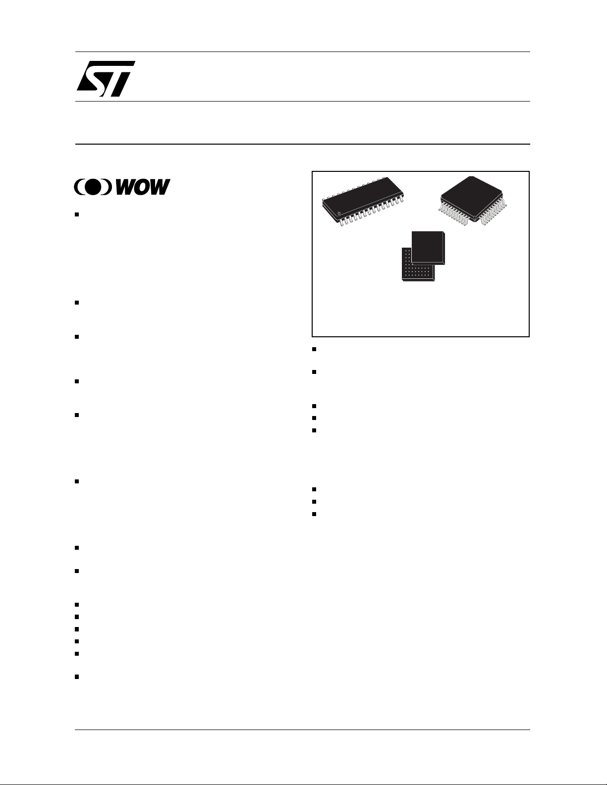
ORDERING NUMBERS: STA014 (SO28)
STA014T (TQFP44)
STA014B (LFBGA 64)
PLL FOR INTERNAL CLOCK AND FOR OUT-
PUT PCM CLOCK GENERATION
CRC CHECK AND SYNCHRONISATION ER-
ROR DETECTION WITH SOFTWARE INDICATORS
I2C CONTROL BUS
LOW POWER 2.4V CMOS TECHNOLOGY
WIDE RANGE OF EXTERNAL CRYSTALS
FREQU ENCIES SUPPORTED
APPLICATIONS
PC SOUND CARDS
MULTIMEDIA PLAYERS
VOICE RECORDERS
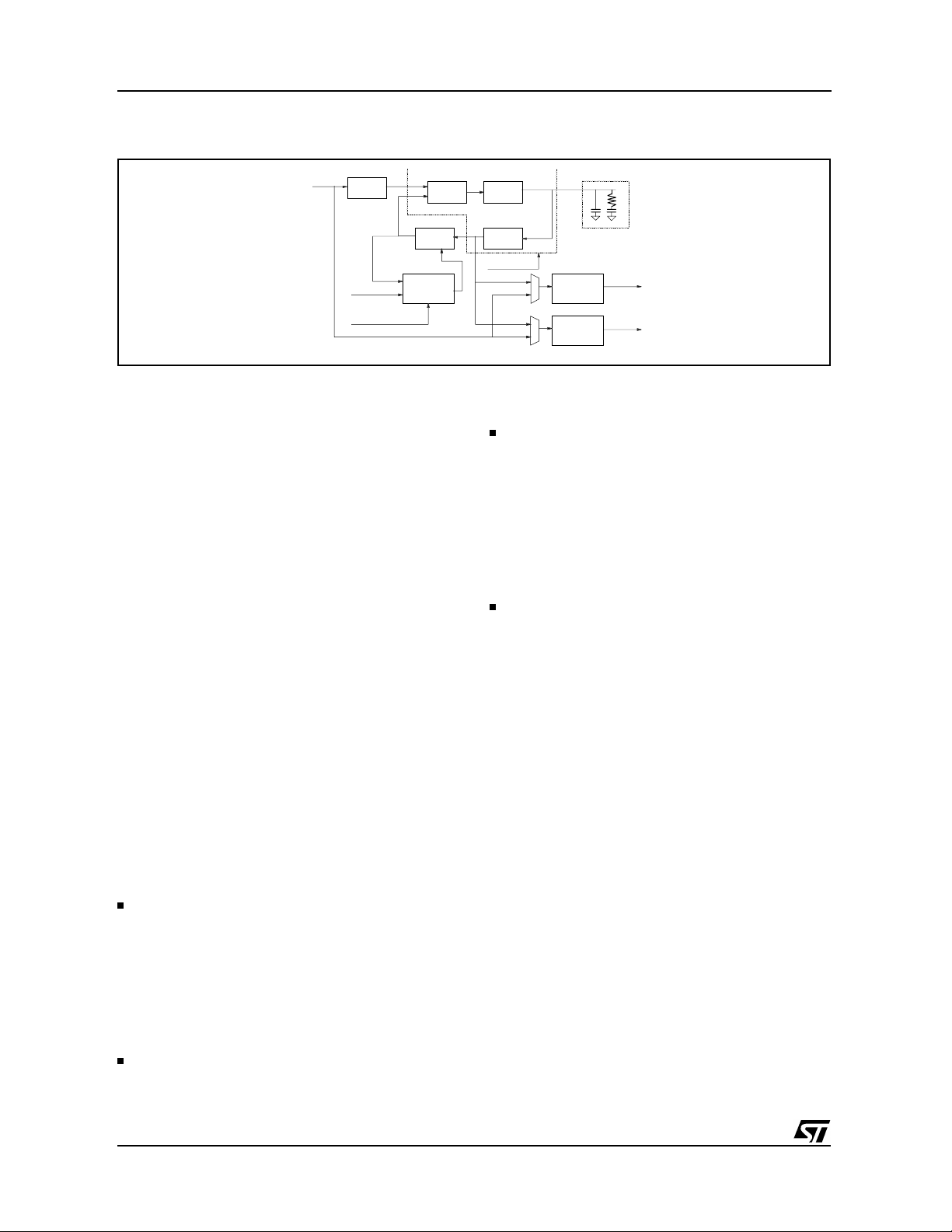
DESCRIPTION
The STA014 is a fully integrated high flexibility
MPEG Layer III Audio Decoder, capable of decoding Layer III compressed elementary streams,
as specified in MPEG 1 and MPEG 2 ISO standards. The device decodes also elementary streams
compre s se d by using low sa m pling rat es, as specified by M PEG 2.5. ST A014 rece ives t h e inpu t dat a
throu gh a Seri al Inp ut Inter face. T he decode d signal is a stereo, mono, or dual channel digital output
that can b e sent di rectl y to a D/ A converter , by the
PCM Output Interface. This interface is software
programmable to adapt the STA014 digital output
to the most commo n DACs architectures used on
the market. The functional STA014 chip partitioning
is described in Fig.1a and Fig.1b.
July 2000
This is preliminary information on a new product now in development or undergoing evaluation. Details are subject to change without notice.
(1)
in order to enable SRS WOW algorithm a mandatory configuration file is required.
1/45
STA014-STA014B-STA014T
Figure 1a. BLOCK DIAGRAM for TQFP44 and LFBGA64 package
SDA SCL
31 32
TQFP44
I2C CONTROL
34
SDI
SCKR
BIT_EN
DATA-REQ
SCK_ADC
LRCK_ADC
SDI_ADC
36
38
27
40
26
24
SERIAL
INPUT
INTERFACE
ADC
INPUT
INTERFACE
25
RESET
BUFFER
256 x 8
PARSER
SYSTEM & AUDIO CLOCKS
15 13 22
XTI XTO FILTTESTEN
MPEG L III
ADPCM
CORE
12
DSP BASED
VOLUME
& TONE
CONTROL
OUTPUT
BUFFER
GPIO
INTERFACE
PCM
OUTPUT
INTERFACE
GPSO
INTERFACE
D99AU1116A
35
20
18
16
14
37
39
41
43
42
44
2
3
4
28
33
STROBE
IODATA
[7:0]
SDO
SCKT
LRCKT
OCLK
GPSO_REQ
GPSO_SCKR
GPSO_DATA
Note: pin numbers refer to TQFP44 only.
Figure 1b. BLOCK DIAGRAM for SO28 package
SDA SCL
34
SO28
I2C CONTROL
5
SDI
SCKR
BIT_EN
DATA-REQ
SCK_ADC
LRCK_ADC
SDI_ADC
6
7
28
8
27
25
SERIAL
INPUT
INTERFACE
ADC
INPUT
INTERFACE
BUFFER
256 x 8
26
RESET
PARSER
SYSTEM & AUDIO CLOCKS
21 20 24
XTI XTO FILTTESTEN
MPEG L III
ADPCM
CORE
DSP BASED
VOLUME
& TONE
CONTROL
19
OUTPUT
BUFFER
PCM
OUTPUT
INTERFACE
D99AU1117A
9
SDO
10
SCKT
11
LRCKT
12
OCLK
2/45
Figure 2. PIN CONNECTIONS
STA014-STA014B-STA014T
VDD_1
VSS_1
BIT_EN
SRC_INT/SCK_ADC
LRCKT
VSS_2
VDD_2
1
N.C.
2
LRCKT
3
OCLK
VSS_2
VDD_2
VSS_3
VDD_3
N.C.
PVDD
PVSS
4
5
6
7
8
9
10
GPSO_REQ
1
2
3
SCKT
SDO
IODATA[7]
4
5
6
7
SO28
8
9
10
11
12
13
D99AU1061
SRC_INT/SCK_ADC
IODATA[6]
SCL
SDI
SCKR
SDO
SCKT
OCLK
44 43 42 41 3940 38 37 36 35 34
BIT_EN
IODATA[5]
28
27
26
25
24
23
22
21
20
19
18
17
16
1514
IODATA[4]
TQFP44
XTI
IODATA[3]
171118 19 20 21 22
N.C.
VSS_4
IODATA[2]
IODATA[1]
12 13 14 15 16
FILT
XTO
OUT_CLK/DATA_REQ
LRCK_ADC
RESETSDA
SDI_ADC
TESTEN
VDD_4
VSS_4
XTI
XTO
FILT
PVSS
PVDD
VDD_3
VSS_3
SDI
GPIO/STROBE
SCKR
33
32
31
30
29
28
27
26
25
24
23
D99AU1062
VDD_4
TESTEN
IODATA[0]
GPSO_DATA
SCL
SDA
VSS_1
VDD_1
GPSO_SCKR
OUT_CLK/DATA_REC
LRCK_ADC
RESET
SDI_ADC
N.C.
12345678
A1 = SDI
A
B
C
D
E
F
G
H
B2 = SCKR
D4 = BIT_EN
D1 = SRC_INT
E2 = SDO
F2 = SCKT
H1 = LRCKT
H3 = OCLK
F3 = VSS_2
E4 = VDD_2
G4 = VSS_3
G5 = VDD_3
F5 = PVDD
G6 = PVSS
D00AU1149
G7 = FILT
G8 = XTO
F7 = XTI
E7 = VSS_4
C8 = VDD_4
D7 = TESTEN
A7 = SDI_ADC
B6 = RESET
A5 = LRCK_ADC
C5 = OUT_CLK/DATA_REQ
B5 = VDD_1
B4 = VSS_1
A4 = SDA
B3 = SCL
C2 = GPIO_STROBE
C3 = IODATA [4]
E3 = IODATA [5]
D2 = IODATA [6]
F1 = IODATA [7]
G3 = GPSO_REQ
F8 = IODATA [3]
F6 = IODATA [2]
E6 = IODATA [1]
C7 = IODATA [0]
C6 = GPSO_SCKR
A2 = GPSO_DATA
LFBGA64
3/45
STA014-STA014B-STA014T
1. OVERVIEW
1.1 - MP3 decoder engine
The MP3 decoder engine is able to decode any
Layer III compliant bitstream: MPEG1, MPEG2
and MPEG2.5 streams are supported. Besides
audio data decoding the MP3 engine also performs ANCILLARY data extraction: these data
can be retrieved via I2C bus by the application
microcontroller in order to implement specific
functions.
Decoded audio data goes through a software volume control and a two-band equalizer blocks before feeding the output I2S interface. This results
in no need for an external audio processor.
MP3 bitstream is sent to the decoder using a simple serial input interface (see pins SDI, SCKR,
BIT_EN and DATA_REQ), supporting input rate
up to 20 Mbit/s. Received data are stored in a
256 bytes long input buffer which provides a
ABSOLUTE MAXIMUM RATINGS
feedback line (see DATA_REQ pin) to the bitstream source (tipically an MCU).
1.2 - ADPCM encoder/decoder engine
This device also embeds a multistandard ADPCM
encoder/decoder supporting different sample
rates (from 8 KHz up to 32 KHz) and different
sample sizes (from 8 bit to 32 bits). During encoding process two different interfaces can be
used to feed data: the serial input interface (same
interface used also to feed MP3 bitstream) or the
ADC input interface, which provides a seamless
connection with an external A/D converter. The
currently used interface is selected via I2C bus.
Also to retrieve encoded data two different interfaces are available: the I2C bus or the faster
GPSO output interface. GPSO interface is able to
output data with a bitrate up to 5 Mbit/s and its
control pins (GPSO_SCKR, GPSO_DATA and
GPSO_REQ) can be configured in order to easily
fit the target application.
Symbol Parameter Value Unit
V
DD
V
i
V
O
T
stg
T
oper
Power Supply -0.3 to 4 V
Voltage on Input pins -0.3 to VDD +0.3 V
Voltage on output pins -0.3 to VDD +0.3 V
Storage Temperature -40 to +150 °C
Operative ambient temp -20 to +85 °C
THERMAL DATA
Symbol Parameter Value Unit
R
th j-amb
Thermal resistance Junction to Ambient 85 °C/W
4/45
STA014-STA014B-STA014T
PIN DESCRIPTION
SO28 TQFP44 LFBGA64 Pin Name Type Function PAD Description
1 29 B5 VDD_1 Supply Voltage
2 30 B4 VSS_1 Ground
3 31 A4 SDA I/O i
4 32 B3 SCL I I
5 34 A1 SDI I Receiver Serial Data CMOS Input Pad Buffer
6 36 B2 SCKR I Receiver Serial Clock CMOS Input Pad Buffer
7 38 D4 BIT_EN I Bit Enable CMOS Input Pad Buffer with
840 D1
SRC_INT/SCK_ADC I Interrupt Line/ADC Serial
9 42 E2 SDO O T ra n s m i t te r S e r ia l D a t a ( P C M D a t a ) CMOS 4mA Output Drive
10 44 F2 SCKT O Transmitter Serial Clock CMOS 4mA Output Drive
11 2 H1 LRCLKT O Transmitter Left/Right Clock CMOS 4mA Output Drive
12 3 H3 OCLK I/O Oversampling Clock for DAC CMOS Input Pad Buffer
13 5 F3 VSS_2 Ground
14 6 E4 VDD_2 Supply Voltage
15 7 G4 VSS_3 Ground
16 8 G5 VDD_3 Supply Voltage
17 10 F5 PVDD PLL Power
18 11 G6 PVSS PLL Ground
19 12 G7 FILT O PLL Filter Ext. Capacitor
20 13 G8 XTO O Crystal Output CMOS 4mA Output Drive
21 15 F7 XTI I Crystal Input (Clock Input) Specific Level Input Pad
22 19 E7 VSS_4 Ground
23 21 C8 VDD_4 Supply Voltage
24 22 D7
TESTEN I Test Enable CMOS Input Pad Buffer with
25 24 A7 SDI_ADC I ADC Data Input CMOS Input Pad Buffer
26 25 B6
RESET I System Reset CMOS Input Pad Buffer with
27 26 A5 LRCK_ADC I ADC Left/Right Clock CMOS Output Pad Buffer
28 27 C5 OUT_CLK/
DATA_REQ
20 C7 IODATA[0] I/O GPIO Data Line CMOS 4mA Schmitt Trigger
18 E6 IODATA[1] I/O GPIO Data Line
16 F6 IODATA[2] I/O GPIO Data Line
14 F8 IODATA[3] I/O GPIO Data Line
37 C3 IODATA[4] I/O GPIO Data Line
39 E3 IODATA[5] I/O GPIO Data Line
41 D2 IODATA[6] I/O GPIO Data Line
43 F1 IODATA[7] I/O GPIO Data Line
35 C2 GPIO_STROBE I/O GPIO Strobe Signal
4 G3 GPSO_REQ O GPSO Request Signal CMOS Output Pad Buffer
28 C6 GPSO_SCKR I GPSO Serial Clock CMOS Input Pad Buffer
33 A2 GPSO_DATA O GPSO Serial Data CMOS Output Pad Buffer
Note: In functional mode TESTEN must be connected to VDD.
2
C Serial Data +
Acknowledge
2
C Serial Clock CMOS Input Pad Buffer
CMOS Input Pad Buffer
CMOS 4mA Output Drive
pull up
CMOS Input Pad Buffer
Clock
CMOS 4mA Output Drive
Conn.
(see paragraph 2.1)
pull up
pull up
O Buffered Output Clock/
CMOS 4mA Output Drive
Data Request Signal
Bidir Pad Buffer
5/45

STA014-STA014B-STA014T
1. ELECTRICAL CHARACTERISTICS:
DD
= 3.3V ±0.3V; T
V
amb
= 0 to 70°C; Rg = 50Ω unless otherwise
specified
DC OPERATING CONDITIONS
Symbol Parameter Value
V
T
GENERAL INTERFACE ELECTRICAL CHARACTERISTICS
Power Supply Voltage 2.4 to 3.6V
DD
Operating Junction Temperature -20 to 125°C
j
Symbol Parameter Test Condition Min. Typ. Max. Unit Note
I
IL
Low Level Input Current
Vi = 0V -10 10
A1
µ
Without pull-up device
I
IH
High Level Input Current
Vi = V
DD
-10 10
A1
µ
Without pull-up device
V
esd
Note 1:
The leakage currents are generally very small, < 1nA. The value given here is a maximum that can occur after an electrostatic stress
on the pin.
Note 2:
Human Body Model.
Electrostatic Protection Leakage < 1µA 2000 V 2
DC ELECTRICAL CHARACTERISTICS
Symbol Parameter Test Condition Min. Typ. Max. Unit Note
V
IL
V
IH
V
ol
V
oh
Low Level Input Voltage 0.2*V
High Level Input Voltage 0.8*V
Low Level Output Voltage I
= Xma 0.4V V 1, 2
ol
High Level Output Voltage 0.85*V
DD
DD
DD
V
V
V 1, 2
Note 1:
Takes into account 200mV voltage drop in both supply lines.
Note 2:
X is the source/sink current under worst case conditions and is reflected in the name of the I/O cell according to the drive capability.
Symbol Parameter Test Condition Min. Typ. Max. Unit Note
I
pu
Pull-up current Vi = 0V; pin numbers 7, 24
RpuEquivalent Pull-up
and 26
-25 -66 -125
50 k
A1
µ
Ω
Resistance
Note 1:
Min. condition: V
Max. condition: V
DD
= 2.7V, 125°C Min process
DD
= 3.6V, -20°C Max.
POWER DISSIPATION
Symbol Parameter Test Condition Min. Typ. Max. Unit Note
PD Power Dissipation
= 2.4V
@ V
DD
Sampling_freq ≤24 kHz 76 mW
Sampling_freq ≤32 kHz 79 mW
Sampling_freq ≤48 kHz 85 mW
6/45

STA014-STA014B-STA014T
Figure 3.
Figure 4.
Test Circuit (refer to SO28 package)
OUT_CLK/DATA_REQ
V
DD
100nF
V
SS
V
DD
100nF
V
SS
V
DD
100nF
V
SS
V
DD
100nF
V
SS
PV
V
DD
DD
PV
V
SS
SS
28
1
2
14
13
16
15
23
22
17 18
100nF4.7µF 4.7µF
PV
DD
Test Load Circuit
V
DD
I
OL
SDA
3
SCL
4
SDO
9
SCKT
10
LRCKT
11
OCLK
12
SDI
5
SCKR
6
BIT_EN
7
SDI_ADC
25
SCR_INT
8
LRCK_ADC
27
XTI
21
XTO
20
19
26
RESET
PV
SS
24
TESTEN
D00AU1143
470pF
10K
1K
4.7nF
PV
SS
Test Load
Output I
OL
SDA 1mA 100pF 3.6V
Other Outputs 100µA100µA 100pF 1.5V
I
OH
C
V
L
REF
OUTPUT
C
I
L
OH
2. FUNCTIONAL DESC RI PTION
2.1 - Clock Signal
The STA014 input clock is derivated from an external source or from a industry standard crystal
oscillator, generating input frequencies of 10,
V
REF
D98AU967
Other frequencies may be supported upon request to STMicroelectronics. Each frequency is
supported by downloading a specific configuration file, provided by STM
XTI is an input Pad with specific levels.
14.31818 or 14.7456 MHz.
Symbol Parameter Test Condition Min. Typ. Max. Unit
V
IL
V
IH
Low Level Input Voltage VDD-1.8 V
High Level Input Voltage VDD-0.8 V
CMOS compatibility
The XTI pad low and high levels are CMOS compatible; XTI pad noise margin is better than typical
CMOS pads.
TTL compatibility
DD
The XTI pad low level is compatible with TTL while the high level is not compatible (for example if V
=
3V TTL min high level = 2.0V while XTI min high level = 2.2V)
7/45
STA014-STA014B-STA014T
Figure 5.
PLL and Clocks Generation System
XTI
N
FRAC
Upda t e FR AC
Switching
Circuit
PFD CP
M
2.2 - PLL & Clock Generator System
When STA014 receives the input clock, as described in Section 2.1, and a valid layer III input
bitstream, the internal PLL locks, providing to the
DSP Core the master clock (DCLK), and to the
Audio Output Interface the nominal frequencies of
the incoming compressed bit stream. The STA014
PLL block dia gram is des cribed in F igure 5.
The audio sample rates are obtained dividing the
oversampling clock (OCLK) by software programmable factors. The operation is done by STA014 embedded softwar e and it is trans parent to the user .
The STA014 PLL can drive directly most of the commercial DACs families, providing an over sampling
clock, OCLK, obtained dividing the VCO frequ ency
with a software programmable dividers.
2.3 - STA014 Operational Modes
The device can be configured in 4 different operational modes. To select one specific mode a
dedicated CHIP_MODE registers is available. For
proper operation the following steps must be issued to switch between different modes:
- issue a software reset (SOFT_RESET register)
- select the desired mode (CHIP_MODE register)
- run the device (RUN register)
Hereby is a short description of each available
mode
ADPCM Encoder
This mode can be used to encode the incoming bitstream with 4 different compression algorithms. Moreover different sample frequencies and word size are supported. For a
detailed description of this features refer to the
related registers.
ADPCM Decoder
This mode can be used when an ADPCM
compressed bitstream must be decoded.
R
CC
VCO
Disable PLL
XTI2OCLK
X
S
XTI2DSPCLK
OCLK
DCLK
The input interface handling and control flow is
the same as in the MP3 Mode.
BYPASS mode
Using this mode it’s possible to use the embedded post-processing controls (volu me and
tone controls) to process an incoming uncompressed stereo audio stream. In this configuration ADC input is the only supported interface.
This could be useful , for instance, to process
audio data coming from an external tuner or
some other auxiliary source.
MP3 mode
In MP3 Mode (default mode) STA014 decodes
the incoming bitstream, acting as a master of
the data communication from the source to itself.
This control is done by a specific buffer management, controlled by STA014 embedded
software. The data coming from the serial interface are stored in the input buffer, a 256
bytes long FIFO.
The feedback line DATA_REQ actually is the
result of the h/w comparison between the writing address of the FIFO and the constant
value 252. This means that if the buffer is f illed
up with more than 252 bytes the DATA_REQ
line goes low, requesting MCU to stop transmission: the maximum time to stop transmitting is given by t he time required to t ransmit 4
bytes (this time, in turn, depends on the bitstream speed used to send MP3 data).
The input interface can receive data with a
speed up to 20Mbit/s. The speed at which the
FIFO is emptied is equ al to the MP3 nominal
bitrate. Provided the FIFO is filled up with 252
bytes the time required to empty it (in worst
condition, which is 320kbit/s mpeg stream) is
about 6ms. So if no more data is received in
this time the buffer will be emptied and this will
badly affect the output audio.
8/45
STA014-STA014B-STA014T
In this mode the fractional part of the PLL is disabled and the audio clocks are generated at
nominal rates. Fig. 6 describes the default
DATA_REQ signal behaviour. Programming
STA014 it is possible to invert the polarity of the
DATA_REQ line (register REQ_POL).
Figure 6.
SOURCE STOPS TRANSMITTING DATA SOURCE STOPS TRANSMITTING DATA
DATA_REQ control line
DATA_REQ
SOURCE SEND DATA TO STA015
D00AU1144
2.4 - STA014 Decoding States
There are three different decoder states:
Init,
and
Decode.
Commands to change the de-
coding states are described in the STA014 I
Idle,
2
registers description.
Idle Mode
In this mode (entered after a S/W or H/W reset)
the decoder is waiting for the RUN command.
This mode should be used to initialize the con-
figuration registers of t he device. The DAC connected to STA014 can be initialized during this
mode (set MUTE to 1).
PLAY MUTE Clock State PCM Output
X 0 Not Running 0
X 1 Running 0
Init Mode
"PLAY" and "MUTE" changes are ignored in this
mode. The internal state of the decoder will be
updated only when the decoder changes from the
state "init" t o the state "decode". The "init" phase
ends when the first decoded samples are at the
output stage of the device.
Decode Mode
This mode is completely described by the following table:
C
PLAY MUTE Clock State
0 0 Not Running 0 No
0 1 Running 0 No
1 0 Running Decoded
1 1 Running 0 Yes
PCM
Output
Samples
Decoding
Yes
Figure 7.
MPEG Decoder Interfaces.
DATA_REQ
SDI
DATA
SOURCE
D98AU912
SCKR
BIT_EN
XTI FILT
XTO
PLL
MPEG
DECODER
SERIAL AUDIO INTERFACE
RX TX
µP
IIC
SCL SDA
IIC
SDO
SCKT
LRCKT
DAC
OCLK
9/45

STA014-STA014B-STA014T
Figure 8.
Serial Input Interface Clocks
SDI
SCKR
SCKR
BIT_EN
D98AU968A
3. INTERFACE DESCRIPTION
3.1 - Serial I nput Interface
STA014 receives the input data (MSB first)
through the Serial Input Interface (Fig.7). It is a
serial communication interface connected to the
SDI (Serial Data Input) and SCKR (Receiver Serial Clock).
The interface can be configured to receive data
sampled on both rising and falling edge of the
SCKR clock. The BIT_EN pin, when set to low,
forces the bitstream input interface to ignore the
incoming data. For proper operation BIT_EN line
should be toggled only when SCKR is stable low
(for both SCLK_POL configuration)8The possible
configurations are described in Fig. 8.
3.2 - GPSO Output Interface
In order to retrieve ADPCM encoded data a General Purpose Serial Output interface is available
(in TQFP44 and LFBGA64 packages only). The
maximum frequency for GPSO_SCKR clock is
Figure 9.
PCM Output Fo rm a ts
LRCKT
SDO
SDO
16 SCLK Cycles
M
S
L
S
16 SCLK Cycles
M
SLS
L
M
S
S
DATA IGNORED
SCLK_POL=0
SCLK_POL=4
DATA IGNOREDDATA VALID
the DSP system clock frequency divided by 3
(i.e. 8.192 MHz @ 24.58MHz). The interface is
based on a simple and configur able 3- lines pr otocol, as described by figure 10.
3.3 - PCM Output Interface
The decoded audio data are output in serial PCM
format. The interface consists of the following signals:
SDO PCM Serial Data Output
SCKT PCM Serial Clock Output
LRCLK Left/Right Channel Selection Clock
The output samples precision is selectable from
16 to 24 bits/word, by setting t he output precision
with PCMCONF (16, 18, 20 and 24 bits mode)
register. Data can be output either with the most
significant bit first (MS) or least significant bit first
(LS), selected by writing into a flag of the
PCMCONF register.
Figure 8 gives a description of the several
STA014 PCM Output Formats. The sample rates
set decoded by STA014 is described in Table 1.
16 SCLK Cycles
L
M
S
S
L
M
S
S
16 SCLK Cycles
M
L
S
S
M
L
S
S
16 SCLK Cycles
PCM_ORD = 0
L
S
PCM_PREC is 16 bit mode
PCM_ORD = 1
M
PCM_PREC is 16 bit mode
S
Table 1:
10/45
LRCKT
SDO
SDO
SDO
SDO
32 SCLK Cycles
M
L
S
S
0
LSM
0
S
M
S
32 SCLK Cycles
M
S
L
0
SMS
M
0
00
S
L
MSBMSB
S
L
00
S
M
S
L
S
M
S
32 SCLK Cycles
L
M
S
S
L
M
0
S
S
M
L
0
S
S
MSL
L
MSB MSB
S
32 SCLK Cycles
32 SCLK Cycles
L
S
M
S
S
00
L
S
PCM_FORMAT = 1
PCM_DIFF = 1
PCM_FORMAT = 0
L
PCM_DIFF = 0
S
PCM_FORMAT = 0
PCM_DIFF = 1
PCM_FORMAT = 1
LSM
PCM_DIFF = 1
M
S
L
0
S
M
0
00
S
S
MPEG Sampling Rates (KHz)
MPEG 1 MPEG 2 MPEG 2.5
48 24 12
44.1 22.05 11.025
32 16 8

Figure 10.
GPSO_SCKR
GPSO_REQ
GPSO_SCKR
GPSO_DATA
GPSO_REQ
STA014-STA014B-STA014T
MCU
GPSO_DATA
To enable the GPSO interface bit GEN of
GPSO_ENABLE register must be set. Using the
GPSO_CONF register the protocol can be configured in order to provide outcoming data on ris-
ADPCM encoding mode to provide an interrupt;
other pins are reserved for future use. The related configuration register is GPIO_CONF. See
the following summary for related pin usage:
D00AU1145
ing/falling edge of GPSO_SCKR input clock; the
GPSO_REQ request signal polarity (usually connected to an MCU interrupt line) can be configured as well.
3.4 ADC Inteface
Name Description Dir
I/ODATA [0]
GPIO data line I/O
....................
I/ODATA [7]
GPIO_STROBE GPIO strobe line I/O
Beside the serial input interface based on SDI
and SCKR lines a 3 wire flexible and user conf ig-
4 ADPCM ENCODING: Overview
urable input interface is also available, suitable to
interface with most A/D converters. To configure
this interface 4 specific I
(ADC_ENABLE, ADC_CONF, ADC_WLEN and
ADC_WPOS). Refer to registers description for
more details.
3.5 General Purpose I/O Interface
A new general purpose I/O interface has been
added to this device (TQFP44 and LFBGA64
only). Actually only the strobe line is used in
INPUT (data to encode) Output (encoded data)
ADC I/F (SDI_ADC + LRCK_ADC + SCK_ADC) GPSO I/F (GPSO_REQ + GPSO_DATA +
ADC I/F (SDI_ADC + LRCK_ADC + SCK_ADC) I
SERIAL I/F (SCKR + SDI + DATA_REQ) GPSO I/F (GPSO_REQ + GPSO_DATA +
SERIAL I/F (SCKR + SDI + DATA_REQ) (*) I
(*) STA013 Compatible mode
2
C registers are available
GPSO_SCKR)
2
GPSO_SCKR)
2
According to the previously described interfaces
there are 4 ways to manage ADPCM data stream
while encoding. Input int erface can be either the
serial receiver block (SDI + SCKR + DATA_REQ
lines) or the ADC specific interface.
Output interfaces can be either t he I
or without interrupt line) or the GPSO high-speed
serial interface (GPSO_REQ + GPSO_ DATA +
GPSO_SCKR lines). This result in the following 4
methods to handle encoding flow:
C + Interrupt (SCL + SDA + DATA_REQ) SO28/TQFP44
C (polling) (SCL + SDA) SO28/TQFP44
Figure. 11
....
I/O
2
C bus (with
Available on
package
TQFP44
LFBGA64
LFBGA64
TQFP44
LFBGA64
LFBGA64
LRCK_ADC
SDI_ADC
SCK_ADC
SDI
SCKR
DATA_REQ
ADC I/F
SERIAL
RECEIVER
ENCOD
ENGINE
GPSOMUX
I2C
D99AU1064
GPSO_REQ
GPSO_DATA
GPSO_SCKR
SDA
SCL
DATA_REQ
11/45
STA014-STA014B-STA014T
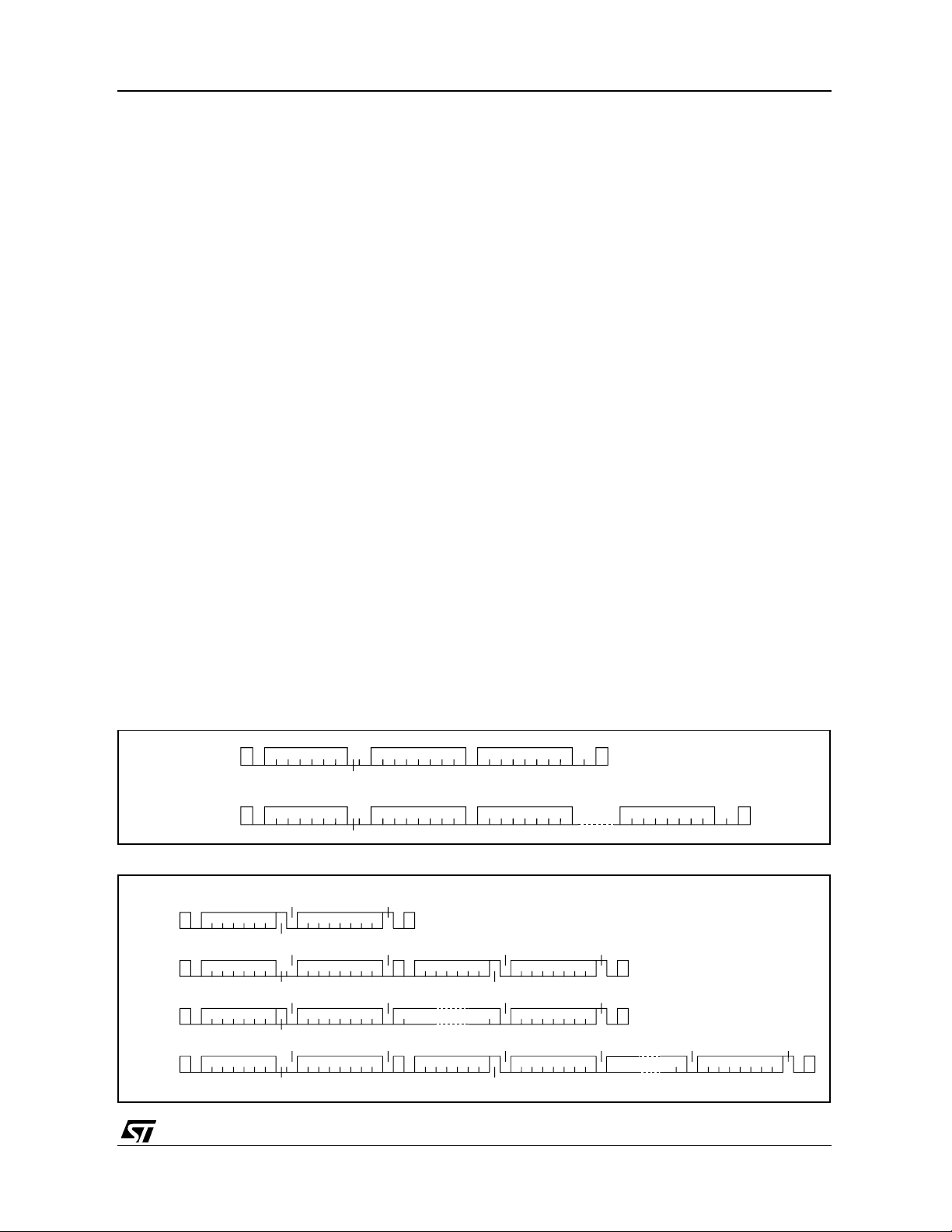
The following 4 figures (fig. 12, 13, 14, 15) show
the available connection diagrams as far as
ADPCM encoding function. As shown in the figures some configuration is not available in SO28
package.
Figure 12.
Input from BITSTREAM, Output from
I2C
SDI
SCKR
DATA_REQ
MCU DAC
BIT_EN
2
C
I
SO28
TQFP44
LFBGA64
LRCKT
SCKT
SDO
OCLK
D99AU1121A
STA013 compatible mode
Figure 14.
Input from BITSTREAM, Output from
GPSO
GPSO_DATA
GPSO_SCKR
GPSO_REQ
SDI
SCKR
DATA_REQ
MCU DAC
BIT_EN
2
C
I
TQFP44
LFBGA64
LRCKT
SCKT
SDO
OCLK
D99AU1122A
Figure 13.
DATA_REQ
MCU
ADC
SLAVE
MCU
ADC
MASTER
Figure 15.
GPSO_SCKR
MCU
ADC
MASTER
Input from ADC, Output from I2C +
IRQ
2
I
C
LRCKT
SCKT
SDO
SDI_ADC
2
C
I
DATA_REQ
LRCK_ADC
SCK_ADC
SDI_ADC
SO28
TQFP44
LFBGA64
SO28
TQFP44
LFBGA64
OCLK
LRCKT
SCKT
SDO
OCLK
Input from ADC, Output from GPSO
GPSO_DATA
GPSO_REQ
LRCK_ADC
SCK_ADC
SDI_ADC
TQFP44
LFBGA64
LRCKT
SCKT
SDO
OCLK
DAC
DAC
D99AU1123A
DAC
D99AU1124A
5 - I2C BUS SPECIFICATION
2
The STA014 supports the I
C protocol. This protocol defines any device that sends data on to the
bus as a transmitter and any device that reads
the data as a receiver. The device that controls
the data transfer is known as the master and the
others as the slave. The master always starts the
transfer and provides the serial clock for synchronisation. The STA014 is always a slave device in
all its communications.
12/45
5. 1 - COMMUNICATION PROTOCOL
5.1.0 - Data transition or change
Data changes on the SDA line must only occur
when the SCL clock is low. SDA transition while
the clock is high are used to identify START or
STOP condition.
5.1.1 - Start condition
START is identified by a high to low transition of
the data bus SDA signal while the clock signal
SCL is stable in the high state.
A START condition must precede any command
for data trans fer.
STA014-STA014B-STA014T
5.1.2 - Stop condition
STOP is identified by low to high transition of the
data bus SDA signal while the clock signal SCL is
stable in the high state. A STOP condition terminates communications between STA014 and the
bus master.
5.1.3 - Acknowledge bit
An acknowledge bit is used to indicate a successful data transfer. The bus transmitter, either master or slave, releases the SDA bus after sending
8 bit of data.
During the 9th clock pulse the receiver pulls the
SDA bus low to acknowledge the receipt of 8 bits
of data.
5.1.4 - Data input
During the data input the STA014 samples the
SDA signal on the rising edge of the clock SCL.
For correct device operation the SDA signal has
to be stable during the rising edge of the clock
and the data can change only when the SCL line
is low.
5.2 - DEVICE ADDRESSIN
G
To start communication between the master and
the STA014, the master must i nitiate with a start
condition. Following this, the master sends onto
the SDA line 8 bits (MSB first) corresponding to
the device select address and read or write
mode.
Figure 16.
Write Mode Sequence
The 7 most significant bits are the device address
identifier, corresponding to the I
2
C bus definition.
For the STA014 these are fixed as 1000011.
The 8th bit (LSB) is the read or write operation
RW, this bit is set to 1 in read mode and 0 for
write mode. After a START condition the STA014
identifies on the bus the device addr ess and, if a
match is found, it acknowledges the identification
on SDA bus during the 9th bit t ime. The following
byte after t he device identification byte is t he internal space address.
5.3 - WRITE OPERATION
(see fig. 16)
Following a START condition the master sends a
device select code with the RW bit set to 0.
The STA014 acknowledges this and waits for the
byte of internal address.
After receiving the internal bytes address the
STA014 again responds with an acknowledge.
5.3.1 - Byte write
In the byte write mode the master sends one data
byte, this is acknowledged by STA014. The master then terminates the transfer by generating a
STOP condition.
5.3.2 - Multibyte write
The multibyte write mode can start from any internal address. The transfer is terminated by the
master generating a STOP condition.
Figure 17.
CURRENT
ADDRESS
READ
START
RANDOM
ADDRESS
READ
START
SEQUENTIAL
CURRENT
READ
START
SEQUENTIAL
RANDOM
READ
START
BYTE
WRITE
MULTIBYTE
WRITE
DEV-ADDR
START
DEV-ADDR
START
Read Mode Sequence
ACK
DEV-ADDR
RW
ACK
DEV-ADDR
RW
RW=
ACK
HIGH
DEV-ADDR
ACK
DEV-ADDR
RW
DATA
SUB-ADDR
DATA
SUB-ADDR
ACK
RW
ACK
RW
NO ACK
ACK
START RW
ACK
ACK
START RW
SUB-ADDR
SUB-ADDR
STOP
DATA
DEV-ADDR
DEV-ADDR
ACK
ACK
ACK
ACK
ACK
DATA IN
DATA IN
DATA
DATA
DATA
ACK
ACK
STOP
NO ACK
NO ACK
ACK
D98AU825B
STOP
STOP
DATA
DATA IN
ACK
ACK NO ACK
D98AU826A
STOP
DATA
STOP
13/45
STA014-STA014B-STA014T
5.4 - READ OPERATION
(see Fig. 17)
5.4.1 - Current byte address read
The STA014 has an internal byte address
counter. Each time a byte is written or read, this
counter is incremented.
For the current byte address read mode, f ollowing a START condition the master sends the device address with the RW bit set to 1.
The STA014 acknowledges this and outputs the
byte addressed by the internal byte address
counter. The master does not acknowledge the
received byte, but terminates the t ransfer with a
STOP condition.
5.4.2 - Sequential address read
This mode can be initiated with either a current
address read or a random address read. However in this case the master does acknowledge
the data byte output and the STA014 continues to
output the next byte in sequence.
To terminate the streams of bytes the master
does not acknowledge the last received byte, but
2
I
C REGISTERS
terminates the transfer with a STOP condition.
The output data stream is from consecutive byte
addresses, with the internal byte address counter
automatically incremented after one byte output.
2
C REGISTERS
6 - I
The following table gives a description of the
MPEG Source Decoder (STA014) register list.
The first column (HEX_COD) is the hexadecimal
code for the sub-address.
The second column (DEC_COD) is the decimal
code.
The third column (DESCRIPTION) is the description of the information contained in the register.
The fourth column (RESET) inidicate the reset
value if any. When no reset value is specifyed,
the default is "undefined".
The fifth column (R/W) is the flag to distinguish
register "read only" and "read and write", and the
useful size of the register itself.
Each register is 8 bit wide. The master shall operate reading or writing on 8 bits only.
HEX_COD DEC_COD DESCRIPTION RESET R/W
$00 0 VERSION R (8)
$01 1 IDENT 0xAC R (8)
$05 5 PLLCTL [7:0] 0xA1 R/W (8)
$06 6 PLLCTL [20:16] (MF[4:0]=M) 0x0C R/W (8)
$07 7 PLLCTL [15:12] (IDF[3:0]=N) 0x00 R/W (8)
$0C 12 REQ_POL 0x01 R/W (8)
$0D 13 SCLK_POL 0x04 R/W (8)
$0F 15 ERROR_CODE 0x00 R (8)
$10 16 SOFT_RESET 0x00 W (8)
$13 19 PLAY 0x01 R/W(8)
$14 20 MUTE 0x00 R/W(8)
$16 22 CMD_INTERRUPT 0x00 R/W(8)
$18 24 DATA_REQ_ENABLE 0x00 R/W(8)
$40 - $51 64 - 81 ADPCM_DATA_1 to ADPCM_DATA_18 0x00 R/W (8)
$40 64 SYNCSTATUS 0x00 R (8)
$41 65 ANCCOUNT_L 0x00 R (8)
$42 66 ANCCOUNT_H 0x00 R (8)
$43 67 HEAD_H[23:16] 0x00 R(8)
$44 68 HEAD_M[15:8] 0x00 R(8)
$45 69 HEAD_L[7:0] 0x00 R(8)
$46 70 DLA 0x00 R/W (8)
$47 71 DLB 0xFF R/W (8)
$48 72 DRA 0x00 R/W (8)
$49 73 DRB 0xFF R/W (8)
$4D 77 CHIP_MODE 0x00 R/W (2)
14/45
 Loading...