

SGS Thomson Microelectronics STA013T, STA013B, STA013 Datasheet
STA013
MPEG 2.5 LAYER III AUDIODECODER
SINGLE CHIP MPEG2 LAYER 3 DECODER
SUPPORTING:
- All features specified for Layer III in ISO/IEC
11172-3(MPEG 1 Audio)
- All features specified for Layer III in ISO/IEC
13818-3.2(MPEG 2 Audio)
- Lowersamplingfrequenciessyntaxextension,
(notspecifiedby ISO) called MPEG2.5
DECODES LAYER III STEREO CHANNELS,
DUAL CHANNEL, SINGLE CHANNEL
(MONO)
SUPPORTING ALL THE MPEG 1 & 2 SAMPLING FREQUENCIES AND THE EXTENSION TO MPEG 2.5:
48, 44.1, 32, 24, 22.05, 16, 12, 11. 025, 8 KHz
ACCEPTS MPEG 2.5 LAYER III ELEMENTARY COMPRESSED BITSTREAM WITH
DATA RATE FROM 8 Kbit/s UP TO 320 Kbit/s
DIGITALVOLUMECONTROL
DIGITALBASS& TREBLECONTROL
SERIALBITSTREAMINPUTINTERFACE
ANCILLARY DATA EXTRACTIONVIA I2C IN-
TERFACE.
SERIAL PCM OUTPUT INTERFACE (I
AND OTHERFORMATS)
PLL FOR INTERNAL CLOCK AND FOR OUT-
PUT PCMCLOCK GENERATION
LOW POWERCONSUMPTION:
85mW AT 2.4V
CRC CHECK AND SYNCHRONISATION ER-
ROR DETECTION WITH SOFTWARE INDICATORS
2
C CONTROLBUS
I
LOW POWER3.3V CMOSTECHNOLOGY
10 MHz, 14.31818 MHz, OR 14.7456 MHz
EXTERNAL INPUT CLOCK OR BUILT-IN INDUSTRY STANDARD XTAL OSCILLATOR
DIFFERENT FREQUENCIES MAY BE SUPPORTED UPON REQUESTTOSTM
APPLICATIONS
PC SOUNDCARDS
MULTIMEDIA PLAYERS
STA013B STA013T
SO28
TQFP44
LFBGA64
2
S
ORDERING NUMBERS: STA013$ (SO28)
STA013T$ (TQFP44)
STA013B$ (LFBGA 8x8)
DESCRIPTION
The STA013 is a fully integrated high flexibility
MPEG Layer III Audio Decoder, capable of decoding Layer III compressedelementary streams,
as specifiedin MPEG1 and MPEG 2 ISO standards. The devicedecodes alsoelementarystreams
compressedby using low samplingrates,as specifiedbyMPEG2.5.
STA013 receives the input data through a Serial
Input Interface. The decoded signal is a stereo,
mono, or dual channel digital output that can be
sent directly to a D/A converter, by the PCM Output Interface. This interface is software programmable to adapt the STA013 digital output to the
most common DACs architectures used on the
market.
The functional STA013 chip partitioning is describedin Fig.1.
November 1999
1/38
STA013 - STA013B - STA013T
Figure 1. Block Diagram:MPEG2.5 LayerIII Decoder HardwarePartitioning.
RESET SDA SCL
26 3 4
I2C CONTROL
5
SDI SDO
SCKR
BIT_EN
6
7
SERIAL
INPUT
INTERFACE
8282120122425
SRC_INT OUT_CLK/DATA_REQ XTI XTO OCLK TESTEN SCANEN
BUFFER
PARSER
SYSTEM &AUDIO CLOCKS TEST INTERFACE
2.5
MPEG
LAYER
DECODER
CORE
III
CHANNEL
CONFIG.
&
VOLUME
CONTROL
OUTPUT
BUFFER
PCM
OUTPUT
INTERFACE
D98AU965
THERMAL DATA
Symbol Parameter Value Unit
R
th j-amb
Thermal resistance Junction to Ambient 85 °C/W
9
10
SCKT
11
LRCKT
ABSOLUTE MAXIMUM RATINGS
Symbol Parameter Value Unit
Power Supply -0.3 to 4 V
Voltage on Input pins -0.3 to VDD+0.3 V
Voltage on output pins -0.3 to VDD+0.3 V
Storage Temperature -40 to +150 °C
Operative ambient temp -20 to +85 °C
2/38
V
DD
V
i
V
O
T
stg
T
oper
Figure 2. Pin Connection
STA013 - STA013B - STA013T
N.C.
LRCKT
OCLK
N.C.
VSS_2
VDD_2
VSS_3
VDD_3
N.C.
PVDD
PVSS
VDD_1
VSS_1
SCL
SDI
SCKR
BIT_EN
SRC_INT
SDO
SCKT
LRCKT
OCLK
VSS_2
VDD_2
1
2
3
4
5
6
7
8
9
10
1
2
3
4
5
6
SO28
7
8
9
10
11
12
13
D98AU911A
SRC_INT
N.C.
SDO
N.C.
SCKT
44 43 42 41 3940 38 37 36 35 34
TQFP44
12 13 14 15 16
XTI
N.C.
FILT
XTO
N.C.
28
27
26
25
24
23
22
21
20
19
18
17
16
1514
N.C.
SCKR
N.C.
BIT_EN
N.C.
171118 19 20 21 22
N.C.
N.C.
N.C.
VSS_4
VDD_4
OUT_CLK/DATA_REQ
VSS_5
RESETSDA
SCANEN
TESTEN
VDD_4
VSS_4
XTI
XTO
FILT
PVSS
PVDD
VDD_3
VSS_3
SDI
33
N.C.
32
SCL
31
SDA
30
VSS_1
29
VDD_1
28
N.C.
27
OUT_CLK/DATA_REC
26
VSS_5
25
RESET
24
SCANEN
23
N.C.
D99AU1019
TESTEN
12345678
A1 = SDI
A
B
C
D
E
F
G
H
B2 = SCKR
D4 = BIT_EN
D1 = SRC_INT
E2 = SDO
F2 = SCKT
H1 = LRCKT
H3 = OCLK
F3 = VSS_2
VDD_2
E4 =
G4 = VSS_3
VDD_3
G5 =
F5 = PVDD
G6 = PVSS
D99AU1085
G7 = FILT
G8 = XTO
F7 = XTI
E7 = VSS4
VDD4
C8 =
D7 = TESTEN
A7 =
SCANEN
B6 = RESET
A5 = VSS5
C5 = OUT_CLK/DATA_REQ
VDD1
B5 =
B4 = VSS1
A4 = SDA
B3 = SCL
LFBGA64
3/38
STA013 - STA013B - STA013T
PIN DESCRIPTION
SO28 TQFP44 LFBGA64 Pin Name Type Function PAD Description
1 29 B5 VDD_1 Supply Voltage
2 30 B4 VSS_1 Ground
3 31 A4 SDA I/O i
4 32 B3 SCL I I
5 34 A1 SDI I Receiver Serial Data CMOS Input Pad Buffer
6 36 B2 SCKR I Receiver Serial Clock CMOS Input Pad Buffer
7 38 D4 BIT_EN I Bit Enable CMOSInputPad Buffer
8 40 D1 SRC_INT I Interrupt Line For S.R. Control CMOS Input Pad Buffer
9 42 E2 SDO O Transmitter SerialData (PCM
10 44 F2 SCKT O Transmitter Serial Clock CMOS 4mA Output Drive
11 2 H1 LRCKT O Transmitter Left/Right Clock CMOS 4mA Output Drive
12 3 H3 OCLK I/O Oversampling Clock for DAC CMOS Input Pad Buffer
13 5 F3 VSS_2 Ground
14 6 E4 VDD_2 Supply Voltage
15 7 G4 VSS_3 Ground
16 8 G5 VDD_3 Supply Voltage
17 10 F5 PVDD PLL Power
18 11 G6 PVSS PLL Ground
19 12 G7 FILT O PLL Filter Ext. Capacitor Conn.
20 13 G8 XTO O Crystal Output CMOS 4mA Output Drive
21 15 F7 XTI I Crystal Input (Clock Input) Specific Level Input Pad
22 19 E7 VSS_4 Ground
23 21 C8 VDD_4 Supply Voltage
24 22 D7 TESTEN I Test Enable CMOSInputPad Buffer
25 24 A7 SCANEN I Scan Enable CMOS Input Pad Buffer
26 25 B6 RESET I System Reset CMOSInputPad Buffer
27 26 A5 VSS_5 Ground
28 27 C5 OUT_CLK/
DATA_REQ
Note: SRC_INT signal is used by STA013 internalsoftware inBroadcast Modeonly;in Multimedia mode SRC_INT must be connected to
In functionalmodeTESTEN must be connected to VDD,SCANEN to ground.
V
DD
2
C Serial Data + Acknowledge CMOS Input Pad Buffer
CMOS 4mA Output Drive
2
C Serial Clock CMOS Input Pad Buffer
withpull up
CMOS 4mA Output Drive
Data)
CMOS 4mA Output Drive
(see paragraph 2.1)
withpull up
withpull up
O Buffered Output Clock/
CMOS 4mA Output Drive
Data Request Signal
4/38

STA013 - STA013B - STA013T
1. ELECTRICALCHARACTERISTICS:VDD=2.4V±0.3V;T
amb
= 0 to 70°C;Rg = 50Ωunlessotherwise
specified
DC OPERATINGCONDITIONS
Symbol Parameter Value
V
T
Power Supply Voltage 2.7 to 3.6V
DD
Operating Junction Temperature -20 to 125°C
j
GENERAL INTERFACE ELECTRICALCHARACTERISTICS
Symbol Parameter Test Condition Min. Typ. Max. Unit Note
I
IL
Low Level Input Current
Vi= 0V -10 10 µA1
Without pull-up device
I
IH
High Level Input Current
Vi=VDD= 3.6V -10 10
A1
µ
Without pull-up device
V
esd
Note 1: The leakage currents are generally very small, < 1nA. The value given here is a maximum thatcan occur after an electrostatic stress
on the pin.
Note 2: Human Body Model.
Electrostatic Protection Leakage < 1µA 2000 V 2
DC ELECTRICAL CHARACTERISTICS
Symbol Parameter Test Condition Min. Typ. Max. Unit Note
V
IL
V
IH
V
ol
V
oh
Low Level Input Voltage 0.2*V
High Level Input Voltage 0.8*VDD V
Low Level Output Voltage Iol= Xma 0.4V V 1, 2
High Level Output Voltage 0.85*V
DD
V
DD
V1,2
Note 1: Takes intoaccount 200mV voltage drop in both supply lines.
Note 2: X is the source/sink current under worst case conditions and is reflected in the name of the I/O cell according to the drive capability.
Symbol Parameter Test Condition Min. Typ. Max. Unit Note
I
pu
R
pu
Pull-up current Vi= 0V; pin numbers 7, 24
Equivalent Pull-up
and 26; V
DD
=3V
-25 -66 -125 µA1
50 kΩ
Resistance
Note 1: Min. condition: VDD= 2.4V, 125°C Min process
Max. condition: V
DD = 3.6V, -20°C Max.
POWERDISSIPATION
Symbol Parameter Test Condition Min. Typ. Max. Unit Note
PD Power Dissipation
@V
=3V
DD
Sampling_freq ≤24 kHz 76 mW
Sampling_freq≤32 kHz 79 mW
Sampling_freq≤48 kHz 85 mW
5/38
STA013 - STA013B - STA013T
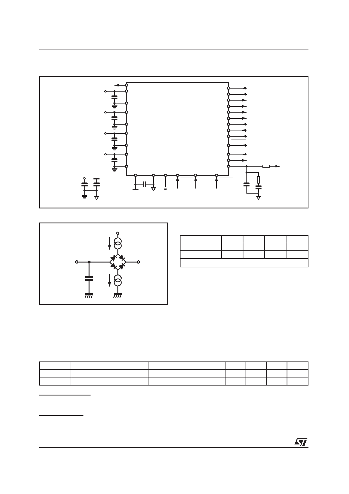
Figure 3. Test Circuit
OUT_CLK/DATA_REQ
4.7µF 4.7µF
V
DD
100nF
V
V
DD
100nF
V
V
DD
100nF
V
V
DD
100nF
V
V
PV
DD
DD
PV
V
SS
SS
Figure 4. Test Load Circuit
I
OL
OUTPUT
SDA
3
24
4
9
10
11
12
5
6
7
8
21
20
19
TESTEN
SCL
SDO
SCKT
LRCKT
OCLK
SDI
SCKR
BIT_EN
SCR_INT
XTI
XTO
470pF
OL
10K
1K
4.7nF
PV
SS
I
OH
C
V
L
REF
1
SS
SS
SS
SS
2
14
13
16
15
23
22
17 18 272826
100nF
PV
V
DD
PV
DD
25
RESET
SS
SCANEN
D98AU966
Test Load
Output I
SDA 1mA 100pF 3.6V
Other Outputs 100µA 100µA 100pF 1.5V
V
REF
C
I
L
OH
D98AU967
2. FUNCTIONALDESCRIPTION
2.1 - Clock Signal
The STA013 input clock is derivated from an external source or from a industry standard crystal
oscillator, generating input frequencies of 10,
14.31818 or 14.7456 MHz.
Other frequencies may be supported upon request to STMicroelectronics. Each frequency is
supported by downloading a specific configuration file, providedby STM
XTI is an input Pad with specific levels.
Symbol Parameter Test Condition Min. Typ. Max. Unit
V
IL
V
IH
Low Level Input Voltage VDD-1.8 V
High Level Input Voltage VDD-0.8 V
CMOS compatibility
The XTI pad low and high levels are CMOS compatible; XTI pad noise margin is better than typical
CMOS pads.
TTL compatibility
The XTI padlow levelis compatiblewith TTL while the high level is not compatible(for example if V
DD =
3V TTL min high level = 2.0V whileXTI min high level = 2.2V)
6/38
Figure 5. MPEG DecoderInterfaces.
STA013 - STA013B - STA013T
µP
DATA_REQ
SDI
DATA
SOURCE
D98AU912
SCKR
BIT_EN
Figure 6. SerialInput Interface Clocks
SDI
SCKR
SCKR
XTO
XTI FILT
PLL
MPEG
DECODER
SERIAL AUDIO INTERFACE
RX TX
IIC
SCL SDA
IIC
DATA IGNORED
SDO
SCKT
LRCKT
DAC
OCLK
SCLK_POL=0
SCLK_POL=4
BIT_EN
D98AU968A
2.2 - SerialInput Interface
STA013 receives the input data (MSB first)
thought the Serial Input Interface (Fig.5). It is a
serial communication interface connected to the
SDI (Serial Data Input) and SCKR (Receiver Serial Clock).
The interface can be configured to receive data
sampled on both rising and falling edge of the
SCKR clock.
The BIT_EN pin, when set to low, forces the bitstream input interface to ignore the incoming
N
data. For proper operation Bit-E
line shold be
toggled only when SCR is stable low (for both
SCLK_POL configuration) The possible configurations are described in Fig. 6.
DATA IGNOREDDATA VALID
2.3 - PLL& ClockGeneratorSystem
When STA013 receives the input clock, as described in Section 2.1, and a valid layer III input
bit stream, the internal PLL locks, providing to the
DSP Core the master clock (DCLK), and to the
Audio Output Interface the nominal frequenciesof
the incoming compressedbit stream.The STA013
PLLblockdiagramisdescribedinFigure7.
The audio sample rates are obtained dividing the
oversampling clock (OCLK) by software programmable factors. The operation is done by STA013
embedded software and it is transparent to the
user.
The STA013 PLL can drive directly most of the
commercial DACs families, providing an over
sampling clock, OCLK, obtained dividingthe VCO
frequencywith a softwareprogrammabledividers.
7/38
STA013 - STA013B - STA013T
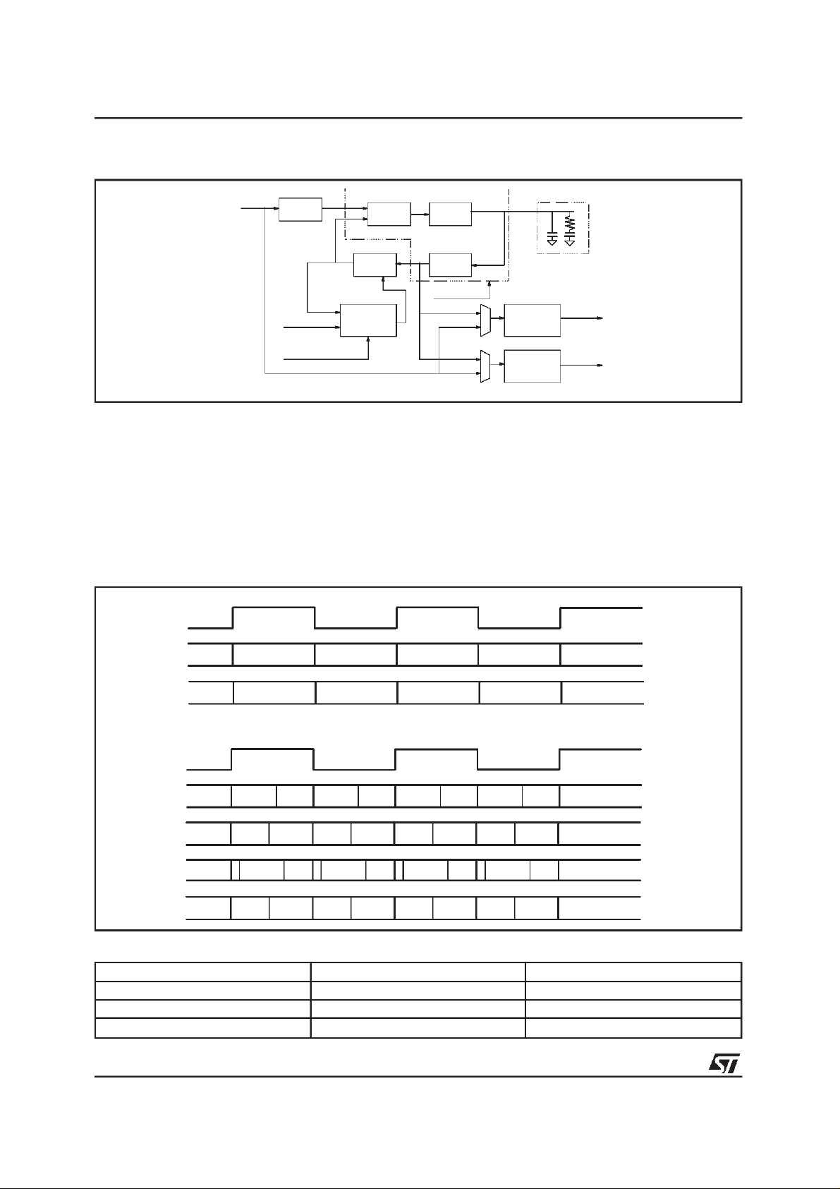
Figure 7. PLL and Clocks GenerationSystem
XTI
N
PFD CP
M
FRAC
Update FR AC
Switching
Circuit
2.4 - PCM Output Interface
The decoded audio data are output in serial PCM
format. The interface consists of the followingsignals:
SDO PCM SerialData Output
SCKT PCMSerial Clock Output
LRCLK Left/RightChannel SelectionClock
The output samples precision is selectable from
Figure 8. PCM Output Formats
16 SCLK Cycles
LRCKT
16 SCLK Cycles
R
CC
VCO
Disable PLL
OCLK
X
XTI2OCLK
DCLK
S
XTI2DSPCLK
16 to 24 bits/word, by settingthe output precision
with PCMCONF (16, 18, 20 and 24 bits mode)
register. Data can be output either with the most
significant bit first (MS) or least significant bit first
(LS), selected by writing into a flag of the
PCMCONFregister.
Figure 8 gives a description of the several
STA013PCM Output Formats.
The sample rates set decoded by STA013 is describedin Table1.
16 SCLK Cycles
16 SCLK Cycles
16 SCLK Cycles
SDO
SDO
M
S
L
S
M
L
S
S
L
M
S
S
32 SCLK Cycles
LRCKT
SDO
SDO
SDO
SDO
M
L
S
S
M
0
S
L
M
0
S
S
M
S
32 SCLK Cycles
M
S
L
S
M
0
00
S
L
MSBMSB MSB MSB
S
Table 1: MPEG SamplingRates (KHz)
MPEG 1 MPEG 2 MPEG 2.5
48 24 12
44.1 22.05 11.025
32 16 8
L
M
S
S
L
M
S
S
32 SCLK Cycles
M
L
S
S
M
L
S
S
PCM_ORD = 0
L
S
PCM_PRECis 16 bit mode
PCM_ORD = 1
M
S
PCM_PRECis 16 bit mode
32 SCLK Cycles
32 SCLK Cycles
L
00
S
L
M
S
S
L
S
L
M
S
S
L
M
S
S
M
00
S
M
0
S
MSL
M
0
L
S
L
00
S
S
L
S
S
M
0
S
L
M
0
S
S
M
S
PCM_FORMAT = 1
0
PCM_DIFF = 1
PCM_FORMAT = 0
L
S
PCM_DIFF = 0
PCM_FORMAT = 0
PCM_DIFF = 1
PCM_FORMAT = 1
L
S
PCM_DIFF = 1
8/38
STA013 - STA013B - STA013T
2.5 - STA013Operation Mode
The STA013 can work in two different modes,
called Multimedia Mode and BroadcastMode.
In Multimedia Mode, STA013 decodes the in-
coming bitstream, acting as a master of the data
communicationfrom the source to itself.
This control is done by a specific buffer management, controlled by STA013embeddedsoftware.
The data source, by monitoring the DATA_REQ
line, send to STA013 the input data, when the
signal ishigh (default configuration).
The communication is stopped when the
DATA_REQline is low.
In this mode the fractional part of the PLL is disabled and the audio clocks are generated at
nominal rates. Fig. 9 describes the default
DATA_REQsignalbehaviour.
Programming STA013 it is possible to invert the
polarity of the DATA_REQ line (register
REQ_POL).
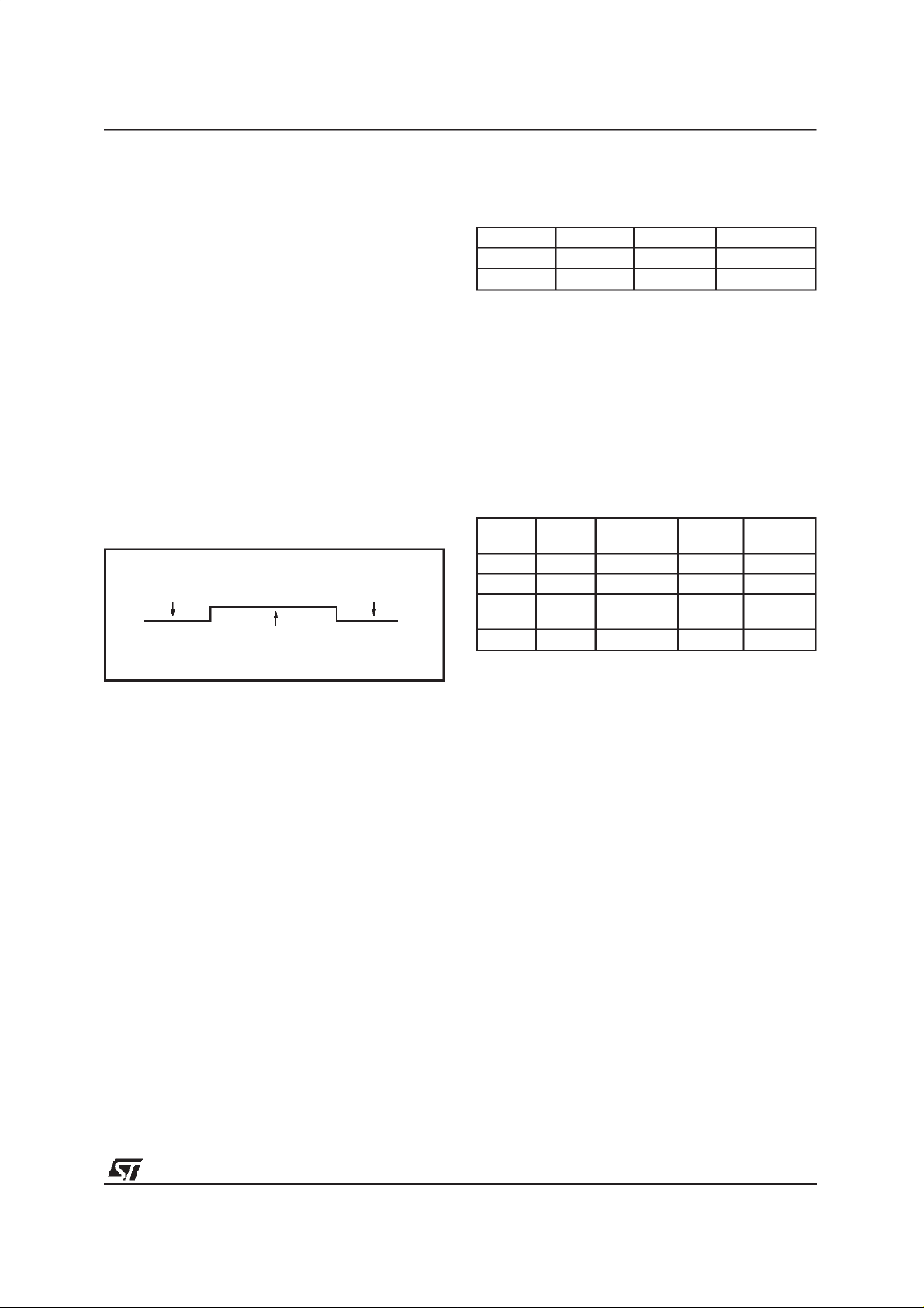
Figure 9.
SOURCE STOPS TRANSMITTING DATA SOURCE STOPS TRANSMITTING DATA
DATA_REQ
SOURCE SEND DATA TO STA013
D98AU913
the configuration register of the device. The DAC
connected to STA013 can be initialised during
this mode (set MUTE to 1).
PLAY MUTE Clock State PCM Output
X 0 Not Running 0
X 1 Running 0
Init Mode
”PLAY” and ”MUTE” changes are ignored in this
mode. The internal state of the decoder will be
updated only when the decoder changes from the
state ”init” to the state ”decode”. The ”init” phase
ends when the first decoded samples are at the
output stage of the device.
Decode Mode
This mode is completely described by the following table:
PLAY MUTE Clock State
0 0 Not Running 0 No
0 1 Running 0 No
1 0 Running Decoded
1 1 Running 0 Yes
PCM
Output
Samples
Decoding
Yes
In Broadcast Mode, STA013 works receiving a
bitstream with the input speed regulated by the
source. In this configuration the source has to
guarantee that the bitrate is equivalent to the
nominal bitrate of the decoded stream.
To compensate the differencebetween the nominal and the real sampling rates, the STA013 embedded software controls the fractional PLL operation. Portable or Mobile applications need
normally to operate in Broadcast Mode. In both
modes the MPEG Synchronisation is automatic
and transparent to the user. To operate in Multimedia mode, the STA013, pin nr. 8, SCR-INT
must be connected to VDD on the application
board.
2.6 - STA013Decoding States
There are three different decoder states: Idle,
Init, and Decode. Commands to change the de-
coding states are described in the STA013 I
2
C
registers description.
Idle Mode
In this mode the decoder is waiting for the RUN
command. This mode should be used to initialise
3-I2C BUS SPECIFICATION
The STA013 supports the I
2
C protocol. This protocol defines any device that sends data on to the
bus as a transmitter and any device that reads
the data as a receiver. The device that controls
the data transfer is known as the master and the
others as the slave. The master always starts the
transfer and provides the serialclock forsynchronisation. The STA013 is always a slave device in
all its communications.
3. 1 - COMMUNICATIONPROTOCOL
3.1.0 - Data transition or change
Data changes on the SDA line must only occur
when the SCL clock is low. SDA transition while
the clock is high are used to identify START or
STOP condition.
3.1.1 - Start condition
START is identified by a high to low transition of
the data bus SDA signal while the clock signal
SCL is stable in the high state.
A START condition must precede any command
fordatatransfer.
9/38
STA013 - STA013B - STA013T
3.1.2 - Stop condition
STOP is identified by low to high transition of the
data bus SDA signal while the clock signal SCL is
stable in the high state. A STOP condition terminates communications between STA013 and the
bus master.
3.1.3 - Acknowledge bit
An acknowledgebit is used toindicate a successful data transfer. The bus transmitter, either master or slave, releases the SDA bus after sending
8 bit of data.
During the 9th clock pulse the receiver pulls the
SDA bus low to acknowledgethe receipt of 8 bits
of data.
3.1.4 - Data input
During the data input the STA013 samples the
SDA signal on the rising edge of the clock SCL.
For correct device operation the SDA signal has
to be stable during the rising edge of the clock
and the data can change only when the SCL line
is low.
3.2 - DEVICEADDRESSING
To start communication between the master and
the STA013, the master must initiate with a start
condition. Following this, the master sends onto
the SDA line 8 bits (MSB first) corresponding to
the device select address and read or write
mode.
Figure 10. Write Mode Sequence
The 7 most significant bits are the device address
identifier, corresponding to the I
2
C bus definition.
For the STA013these are fixed as 1000011.
The 8th bit (LSB) is the read or write operation
RW, this bit is set to 1 in read mode and 0 for
write mode. After a STARTcondition the STA013
identifies on the bus the device address and, if a
match is found, it acknowledgesthe identification
on SDA bus during the 9th bittime. The following
byte after the device identification byte is the internal space address.
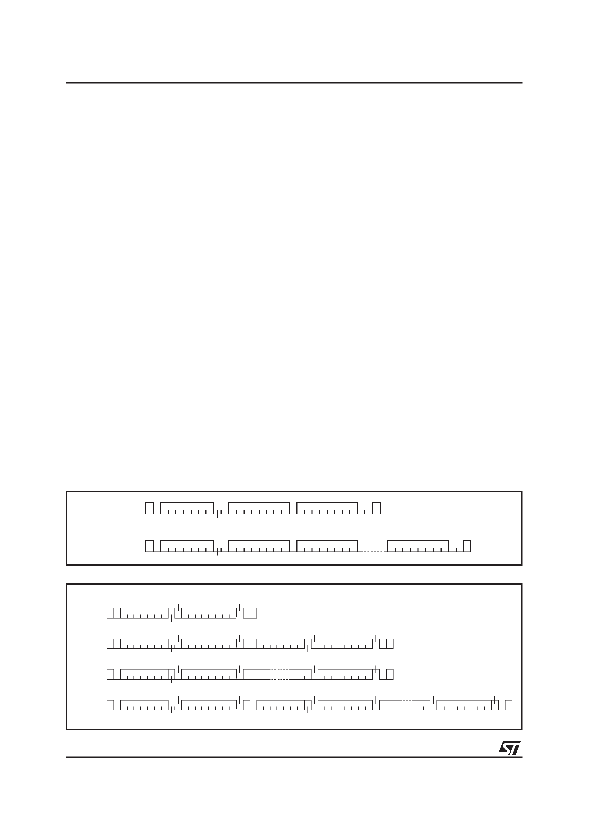
3.3 - WRITEOPERATION(see fig. 10)
Following a START condition the master sends a
deviceselectcode with the RW bit set to 0.
The STA013 acknowledges this and waits for the
byte ofinternal address.
After receiving the internal bytes address the
STA013again responds with an acknowledge.
3.3.1 - Byte write
In the bytewrite mode the mastersends one data
byte, this is acknowledged by STA013. The master then terminates the transfer by generating a
STOP condition.
3.3.2 - Multibytewrite
The multibyte write mode can start from any internal address. The transfer is terminated by the
master generatinga STOPcondition.
BYTE
WRITE
MULTIBYTE
WRITE
START
START RW
DEV-ADDR
DEV-ADDR
Figure 11. Read Mode Sequence
ACK
CURRENT
ADDRESS
RANDOM
ADDRESS
SEQUENTIAL
CURRENT
SEQUENTIAL
RANDOM
10/38
READ
READ
READ
READ
DEV-ADDR
START
DEV-ADDR
START RW
START
START RW
DEV-ADDR
DEV-ADDR
RW=
HIGH
DATA
RW
ACK
SUB-ADDR
ACK
DATA
ACK
SUB-ADDR
ACK
RW
ACK
NO ACK
ACK
START RW
ACK
ACK
START RW
SUB-ADDR
SUB-ADDR
STOP
DATA
DEV-ADDR
DEV-ADDR
ACK
ACK
ACK
ACK
ACK
DATA IN
DATA IN
DATA
DATA
DATA
ACK
ACK
STOP
NO ACK
NO ACK
ACK
D98AU825B
STOP
STOP
DATA
DATA IN
ACK
ACK NO ACK
D98AU826A
STOP
DATA
STOP
STA013 - STA013B - STA013T
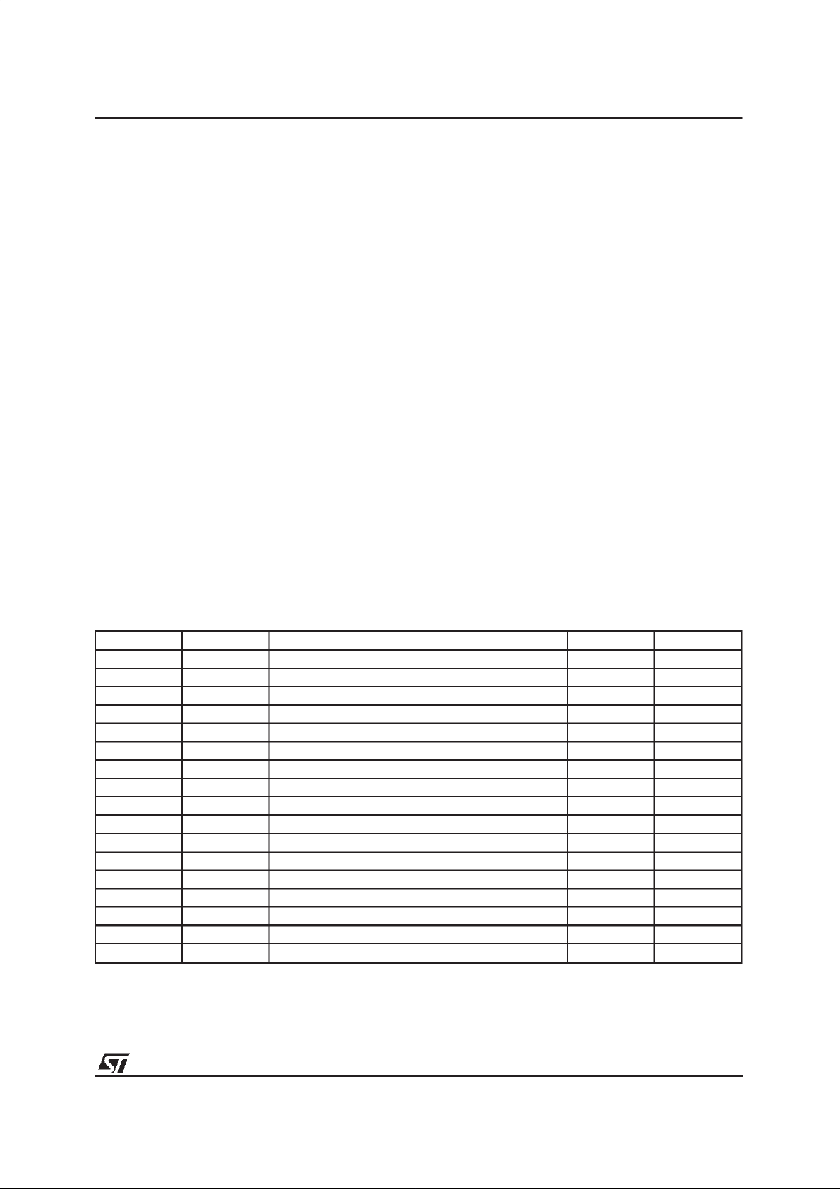
3.4 - READOPERATION(see Fig. 11)
3.4.1 - Currentbyte addressread
The STA013 has an internal byte address
counter. Each time a byte is written or read, this
counter is incremented.
For the current byte address read mode, following a START condition the master sends the device addresswith the RW bit setto 1.
The STA013 acknowledges this and outputs the
byte addressed by the internal byte address
counter. The master does not acknowledge the
received byte, but terminates the transfer with a
STOP condition.
3.4.2 - Sequentialaddress read
This mode can be initiated with either a current
address read or a random address read. However in this case the master does acknowledge
the data byte output and the STA013 continues to
output the next byte in sequence.
To terminate the streams of bytes the master
does not acknowledgethe last received byte, but
terminatesthe transfer with a STOP condition.
The output data stream is from consecutive byte
addresses, with the internal byte address counter
automaticallyincrementedafter one byte output.
2
4-I
C REGISTERS
The following table gives a description of the
MPEGSource Decoder (STA013)register list.
The first column (HEX_COD) is the hexadecimal
code for the sub-address.
The second column (DEC_COD) is the decimal
code.
The third column (DESCRIPTION) is the description of the informationcontained in the register.
The fourth column (RESET) inidicate the reset
value if any. When no reset value is specifyed,
the default is ”undefined”.
The fifth column (R/W) is the flag to distinguish
register ”read only” and ”read and write”, and the
useful size of the register itself.
Each register is 8 bitwide. The master shall operate readingor writing on 8 bits only.
2
I
C REGISTERS
HEX_COD DEC_COD DESCRIPTION RESET R/W
$00 0 VERSION R (8)
$01 1 IDENT 0xAC R (8)
$05 5 PLLCTL [7:0] 0xA1 R/W (8)
$06 6 PLLCTL [20:16] (MF[4:0]=M) 0x0C R/W (8)
$07 7 PLLCTL [15:12] (IDF[3:0]=N) 0x00 R/W (8)
$0B 11 reserved
$0C 12 REQ_POL 0x01 R/W (8)
$0D 13 SCLK_POL 0x04 R/W (8)
$0F 15 ERROR_CODE 0x00 R (8)
$10 16 SOFT_RESET 0x00 W (8)
$13 19 PLAY 0x01 R/W(8)
$14 20 MUTE 0x00 R/W(8)
$16 22 CMD_INTERRUPT 0x00 R/W(8)
$18 24 DATA_REQ_ENABLE 0x00 R/W(8)
$40 64 SYNCSTATUS 0x00 R (8)
$41 65 ANCCOUNT_L 0x00 R (8)
$42 66 ANCCOUNT_H 0x00 R (8)
11/38

STA013 - STA013B - STA013T
I2C REGISTERS (continued)
HEX_COD DEC_COD DESCRIPTION RESET R/W
$43 67 HEAD_H[23:16] 0x00 R(8)
$44 68 HEAD_M[15:8] 0x00 R(8)
$45 69 HEAD_L[7:0] 0x00 R(8)
$46 70 DLA 0x00 R/W (8)
$47 71 DLB 0xFF R/W (8)
$48 72 DRA 0x00 R/W (8)
$49 73 DRB 0xFF R/W (8)
$50 80 MFSDF_441 0x00 R/W (8)
$51 81 PLLFRAC_441_L 0x00 R/W (8)
$52 82 PLLFRAC_441_H 0x00 R/W (8)
$54 84 PCM DIVIDER 0x03 R/W (8)
$55 85 PCMCONF 0x21 R/W (8)
$56 86 PCMCROSS 0x00 R/W (8)
$59 89 ANC_DATA_1 [7:0] 0x00 R (8)
$5A 90 ANC_DATA_2 [15:8] 0x00 R (8)
$5B 91 ANC_DATA_3 [23:16] 0x00 R (8)
$5C 92 ANC_DATA_4 [31:24] 0x00 R (8)
$5D 93 ANC_DATA_5 [39:32] 0x00 R (8)
$61 97 MFSDF (X) 0x07 R/W (8)
$63 99 DAC_CLK_MODE 0x00 R/W (8)
$64 100 PLLFRAC_L 0x46 R/W (8)
$65 101 PLLFRAC_H 0x5B R/W (8)
$67 103 FRAME_CNT_L 0x00 R (8)
$68 104 FRAME_CNT_M 0x00 R (8)
$69 105 FRAME_CNT_H 0x00 R (8)
$6A 106 AVERAGE_BITRATE 0x00 R (8)
$71 113 SOFTVERSION R (8)
$72 114 RUN 0x00 R/W (8)
$77 119 TREBLE_FREQUENCY_LOW 0x00 R/W (8)
$78 120 TREBLE_FREQUENCY_HIGH 0x00 R/W (8)
$79 121 BASS_FREQUENCY_LOW 0x00 R/W (8)
$7A 122 BASS_FREQUENCY_HIGH 0x00 R/W (8)
$7B 123 TREBLE_ENHANCE 0x00 R/W (8)
$7C 124 BASS_ENHANCE 0x00 R/W (8)
$7D 125 TONE_ATTEN 0x00 R/W (8)
Note:
1) The HEX_COD is the hexadecimal adress that the microcontroller has togenerate to access the information.
2) RESERVED: register used forproduction test only, or for future use.
12/38
 Loading...