


®
FRON T_ END INT ERFACE:
IF input carrier frequency: f = 1.84 MHz
Single internal 6 bit A/D converter
QPSK demodulation
Input symbol frequency: Fs = 1.84 Msymbols/s
Digital Nyquist root filter:
- roll-off value of 0.4
Digital carrier loop:
- on-chip quadrature demodulator and tracking
loop
- lock detector
- C/N indicator
Digital timing recovery:
- internal timing error evaluation, filter and
correction
Digital AGC:
- internal signal power estimation and filter
- output control signal for AGC (1 bit PWM)
FORWARD ERROR CORRECTION :
Inner decoder:
- Viterbi soft decoder for convolutional codes,
constraint length M=7, Rate 1/2
Deinterleaver block
Outer decoder:
- Reed-Solomon decoder for 32 parity bytes;
correction of up to 16 byte errors
- Block lengths: 255
- Energy dispersal descrambler
BACK_END INTERFACE:
Broadcast Channel selection
Audio Service Component selection to MPEG
decoder
Service Component selection
CONTROL:
I2C serial Bus control interface
STA002
STARMAN CHANNEL DECO DE R
TQFP44
DECRYPTION:
WES scheme supported
DESCRIPTION
Designed for World Space satellites digital audio
receivers, the STA002 Digital Receiver Front-end
integrates all the blocks needed to demodulate
incoming digital satellite audio signals from the
tuner: analog to digital converter, QPSK demodulator, signal power estimator, automat ic gain control, Viterbi decoder, deinterleaver, Reed-Solomon decoder and energy dispersal descrabler. Its
advanced error correction functions guarantees a
low error rate even with small low gain receiver
antennas.
Additional functions include the selection of
broadcast channel, service components and
audio components for source decoding:
- The MPEG Audio bitstream is provided at the
serial audio output port.
- The Broadcast Channel is provided to the serial
data output port.
- The Service Component is provided at the SC
output interface.
World Space encryption scheme is supported for
pay programs and paging.
January 2002
1/43
STA002
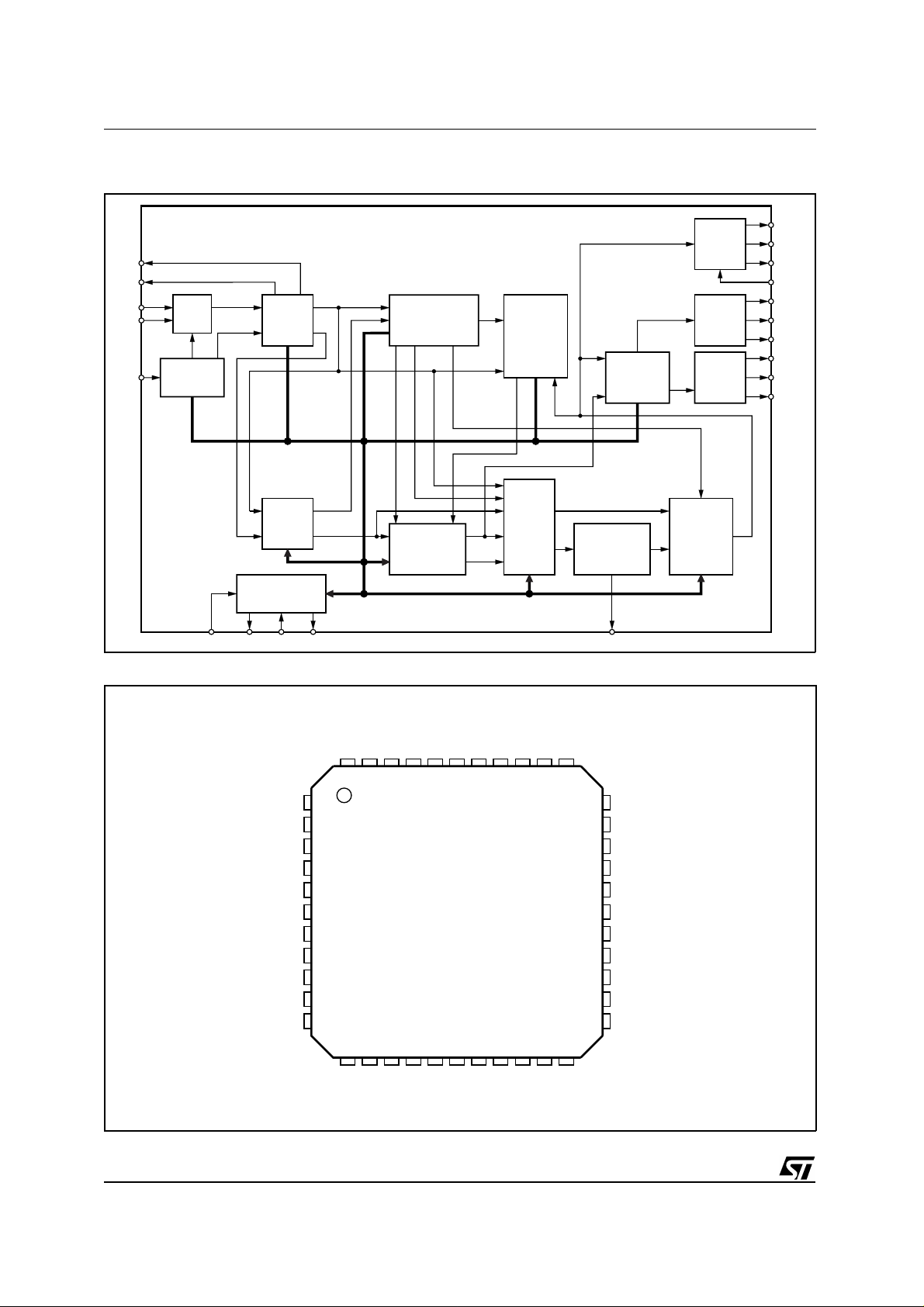
Fig. 1: Channel Decoder Block Diagram
LOCK
AGC
RXI
RNXI
M_CLK
A/D
PLL/CLOCK
DISTRIBUTION
MICROPROCESSOR
INTRRESET MINTR
Fig. 2: Pin Connection
QPSK
FRAME
SYNC.
INTERFACE
SCL
TDM_CLK
SDA
TDM
TDM FRAME
CONTROLLER
PRC
MANAGEMENT
BC_CLK
TSCC
MANAGEMENT
VITERBI
BC
MANGEMENT
DE-INTERLEAVER
BC
DATA
INTERFACE
SC
DATA
INTERFACE
SC
SOURCE
DECODER
INTERFACE
REED
SOLOMON
D96AU541C
BCCK
BCDO
BCSYNC
BCDIN
SCEN
SCDO
SCCK
SCK
SDO
SEN
BC/TSCC
2/43
TEST 1
AGC
VDD
A_VDD
RXI
NRXI
A_GND
GND
M_CLK
CLK_TEST
TEST 2
SCEN
VDD
BCDO
BCCK
TEST 8
TEST 9
SCDO
GND
SCCK
VDD
GND
44 43 42 41 3940 38 37 36 35 34
1
2
3
4
5
6
7
8
9
10
12 13 14 15 16
VDD
LOCK
TEST 3
171118 19 20 21 22
SCL
SDA
GND
INTR
GND
VDD
RESET
TEST 4
33
32
31
30
29
28
27
26
25
24
23
TEST 7
BCDIN
BCSYNC
GND
SDO
SCK
SEN
VDD
TEST 6
MINTR
TEST 5
D97AU671A

PIN DESCRIPTION
Type Pin Name Type Function PAD Description
1, 11, 12 TEST (1:3) I Test Pin CMOS Input Pad Buffer with Pull-Down
22 23 , 25 , 3 3, 3 4 , 44 TEST
2 AGC O AGC Output CMOS 2mA Output Driver
3, 14, 21,
VDD Positive Supply Voltage
26, 38, 40
4 A_VDD Analog Positive Supply Voltage
5 RXI I IF Signal Input Analog Pad Buffer
6 NRXI I IF Signal Input Analog Pad Buffer
7 A_GND Analog Ground
9 M_CLK I Master Clock Analog Pad Buffer with Comparator
10 CLK_TEST Not Connected CMOS Input Pad Buffer
13 LOCK O Carrrier Lock Indicator CMOS 2mA Output Driver
15 SDA I/O Data + ACK CMOS Schmitt Trigger Bdir Pad Bufer
16 SCL I Serial Clock CMOS Input Pad Schmitt Triggered
8, 17, 19,
GND Negative Supply Voltage
30, 35, 42
18 INTR O Interrupt CMOS 2mA Output Driver
20 RESET I Master Reset CMOS Input Pad Buffer with Pull-Up
24 MINTR O MPEG Interrupt CMOS 2mA Output Driver
27 SEN O MPEG Enable CMOS 2mA Output Driver
28 SCK O MPEG Clock CMOS 2mA Output Driver
29 SDO O MPEG Bit Output CMOS 2mA Output Driver
31 BCSYNC O Broadcast Channel Sync CMOS 2mA Output Driver
32 BCDIN I Broadcast Channel Data Input CMOS Input Pad Buffer
36 BCCK O Broadcast Channel Clock CMOS 2mA Output Driver
37 BCDO O Broadcast Channel Data Output CMOS 2mA Output Driver
39 SCEN O Service Component Enable CMOS 2mA Output Driver
41 SCCK O Service Component Clock CMOS 2mA Output Driver
43 SCDO O Service Component Data Output CMOS 2mA Output Driver
Note: pin 1, 11, 12 and 22 must be connected to ground in functional mode.
I Test Pin
(4:9)
STA002
THERMAL DATA
Symbol Parameter Value Unit
R
th j-amb
Thermal resistance Junction to Ambient 85 °C/W
ABSOLUTE MAXIMUM RATINGS
Symbol Parameter Value Unit
V
DD
V
i
V
O
T
stg
T
oper
Power Supply -0.3 to 4 V
Voltage on Input pins -0.3 to VDD +0.3 V
Voltage on output pins -0.3 to VDD +0.3 V
Storage Temperature -40 to +150 °C
Operative ambient temp -20 to +85 °C
3/43

STA002
ELECTRICAL CHARACTERISTICS:
DD
= 3.3V ±0.3V; T
V
amb
= 0 to 70°C; Rg = 50Ω unless otherwise
specified
DC OPERATING CONDITIONS
Symbol Parameter Value
V
T
GENERAL INTERFACE ELECTRICAL CHARACTER IST ICS
Power Supply Voltage 2.7 to 3.6V
DD
Operating Junction Temperature -20 to 125°C
j
Symbol Parameter Test Condition Min. Typ. Max. Unit Note
I
IL
Low Level Input Current
Vi = 0V -10 10
A1
µ
Without pull-up device
I
IH
High Level Input Current
Vi = V
DD
-10 10
A1
µ
Without pull-up device
V
esd
The leakage currents are generally very small, < 1nA. The value given here is a maximum that can occur after an electrostatic stress
Note 1 :
on the pin.
Human Body Model.
Note 2:
Electrostatic Protection Leakage < 1µA 2000 V 2
DC ELECTRICAL CHARACTERISTICS
Symbol Parameter Test Condition Min. Typ. Max. Unit Note
V
IL
V
IH
V
ol
V
oh
Low Level Input Voltage 0.2*V
High Level Input Voltage 0.8*V
Low Level Output Voltage I
= Xma 0.4V V 1, 2
ol
High Level Output Voltage 0.85*V
DD
DD
DD
V
V
V 1, 2
Takes into account 200mV voltage drop in both supply lines.
Note 1:
X is the source/sink current under worst case conditions and is reflected in the name of the I/O cell according to the drive capability.
Note 2:
PULL_UP & PULL_DOWN CHARACTERISTICS
Symbol Parameter Test Condition Min. Typ. Max. Unit Note
I
pu
Pull-up current Vi = 0V -25 -66 -125
IpuPull-up current Vi = V
RpuEquivalent Pull-up
Vi = 0V 50 k
DD
25 66 125
A1
µ
A1
µ
Ω
Resistance
R
pu
Equivalent Pull-down
Vi = V
DD
50 k
Ω
Resistance
Min. condition: V
Note 1:
Max. condition: V
DD
= 2.7V, 125°C Min process
DD
= 3.6V, -20°C Max.
M_ CLK Electrical Characteristics (Pin number 9)
Symbol Parameter Min. Typ. Max. Unit
V
il
V
ih
V
ref
Low Level Input Voltage VDD -1.7 V
High Level Input Voltage VDD -0.9 V
Input Reference Voltage VDD -1.3 V
POWER DISSIPATION
Symbol Parameter Test Condition Min. Typ. Max. Unit Note
PD Power Dissipation
= 3V
@ V
DD
M_CLK = 39,0269MHz 80 mW
4/43

Fig. 3: Test Circuit
STA002
VDD
VDD
VDD
VDD
VDD
VDD
AVDD
TEST1
RXI
NRXI
M_CLK
TEST_CLK
TEST2
100nF
100nF
100nF
100nF
100nF
100nF
3
8
14
17
21
19
26
30
38
35
40
42
4
7
1
5
6
9
10
11
44
34 TEST8
33 TEST7
32 BCDIN
25 TEST6
23 TEST5
22 TEST4
20 RESET
16 SCL
15 SDA
12 TEST3
200
43
200
41 SCCK
200
39 SEN
200
37 BCDO
200
36 BCCK
200
31
200
29 SDI
200
28 SCK
200
27 SEN
200
24 MINTR
200
18 INTR
200
2
200
13
TEST9
SCDI
BCSYNC
AGC
LOCK
VDD
4.7µF 4.7µF100nF 100nF 100nF 100nF 100nF
Figure 4.
OUTPUT
V
SS
Test Load Circuit
C
L
V
SS
V
SS
V
DD
I
OL
V
REF
I
OH
D98AU967
AVDD
4.7µF 4.7µF100nF
AV
SS
AV
SS
100nF 100nF 100nF 100nF
AV
SS
D99AU1011
Test Load
Output I
OL
SDA 5mA 100pF 3.6V
Other Outputs 100µA 100µA 100pF 1.5V
I
OH
C
L
V
REF
5/43

STA002
FUNCTIONAL DESCRIPTION
The STA002 integrates all the functions needed
to demodulate the signal coming from the RF FE;
with reference to the block diagram (Fig 1),
STA002 includes the following functions:
Microprocessor interface
Data transmission from microcontroller to the de-
vice takes place through the 2 wires (SDA and
SCL) I2C bus interface. STA002 acts always as a
slave in all its communications.
Interface to the Front-end
This block receives from the RF front-end the
QPSK modulated signal, centered at 1.84 MHz
(2nd IF frequency). This signal is over sampled
using the Master Clock and converted to digital
on 6 bits in 2’s complement format. The same frequency is also used to provide the clock signal for
the QPSK demodulator block.
QPSK
This block is composed by:
- AGC1
- quadrature demodulator
- carrier recovery
- timing recovery
- frequency sweep generator
- AGC2
- lock indicator
- carrier to noise estimator
To assure flexibility and to cover different working
conditions most of the parameters of each function can be programmed through the I2C interface.
TDM Demultiplexer
The TDM frame is divided into 3 fields.
The first is the Master Frame Preamble (MFP)
which contains the synchronisation word. The
second, the Time Slot Control Channel (TSCC),
contains information about the or ganiz ation of the
Prime Rate Channel data which follows. The
third, is the data field; it contains 96 Prime Rate
Channels of 16 Kbit/s each; up to 8 Prime Rate
Channels are grouped into one Broadcast Channel.
The TDM demultiplexer executes the extraction
and decoding of one Broadcast Channel from the
TDM stream, according to the instructions coming from the microcontroller. The decoding flow is
the following:
- TDM synchronization
The master frame synchronization block receives
the demodulated symbol stream from the QPSK
demodulator and performs the alignment detecting the Master Frame Preamble.
The known syncronization word is also used to
correct the phase ambiguity intrinsic in QPSK demodulation.
- TSCC extraction
The information of the Prime Rate Channels to
Broadcast Channels allocation are contained in
the TSCC field which is synchronised with the
MFP.
In this stage all the information related to the
TSCC are extracted and made available for the
microcontroller via the I2C interface.
- PRC extraction and BC recovery
This block, after the Broadcast Channel (BC) se-
lection, performs the extrac tion and synchronisation of the Prime Rate Channels (PRC) belonging
to the selected BC.
The extracted PRCs are aligned and grouped into
one BC data stream.
- FEC decoder
The extracted BC is decoded using a concate-
nated Forward Error Correction approach.
The FEC circuitry utilizes three error correction
stages: a rate 1/2 Viterbi decoder, a 255x4 bytes
convolutional deinterleaver and a 255/223 Reed
Solomon decoder.
The RS input blocks are 255 bytes long with 32
parity bytes.
Up to 16 errored bytes can be fixed in each RS
block.
BC demultiplexer
Every BC contains up to 8 Service Components;
the Service Control Header (SCH) field contains
all the information related to the organization of
the Service Components. This stage provides the
extraction of the SCH from the BC.
The SCH is available through I2C bus to the microcontroller for the selection of the desired Audio
Service Component, which is then supplied directly to the MPEG Source decoder via the audio
Service Component Interface.
DEVICE OPERATION
2
1. I
C BUS SPECIFICATION
The STA002 supports the I2C protocol. This protocol defines any device that sends data on to the
bus as a transmitter and any device that reads
the data as a receiver. The device that controls
the data transfer is known as the master and the
others as the slave. The master will always initiate the transfer and will provide the serial clock
6/43

STA002
for synchronisation. The STA002 is always a
slave device in all its communications.
COMMUNICATION PROTOCOL
1. 1
1.1.0 Data transition or change
Data changes on the SDA line must only occur
when the SCL clock is low. SDA transitions while
the clock is high are used to identify START or
STOP condition.
1.1.1 Start condition
START is identified by a high to low t ransition of
the data bus SDA signal while the clock signal
SCL is stable in the high state. A START condition must precede any command for data transfer.
1.1.2 Stop condition
STOP is identified by low to high transition of the
data bus SDA signal while the clock signal SCL is
stable in the high state. A STOP condition terminates communications between STA002 and the
bus master.
1.1.3 Acknowledge bit
An acknowledge bit is used to indicate a success-
ful data transfer. The bus transmitter, either master or slave, will r elease the SDA bus aft er sending 8 bits of data.
During the 9th clock pulse the receiver pulls the
SDA bus low to acknowledge the receipt of 8 bits
of data.
Some registers do not give acknowledge when
the data is not available.
(RW; set to 1 in read mode and to 0 in write
mode). After a START condition the STA002
identifies on the bus the device address and if
matching it will acknowledges the identification on
SDA bus during the 9th bit time.
The following 2 bytes after t he device identification byte are the internal space address.
1.3 WRITE OPERATION (see fig. 5)
Following a START condition the master sends a
device select code with the RW bit set to 0.
The STA002 gives the acknowledge and waits for
the 2 bytes of internal address. The least significant 10 bits of t he 2 bytes address provides access to any of the internal registers. The most
significant bit means incremental mode (1 =
autoincremental, 0 = no) and the other bits are
set to zero.
After the receiption of each of the internal bytes
address the STA002 again responds with an acknowledge.
1.3.1 Byte write
In the byte write mode the master sends one data
byte and this is acknowledged by STA002. The
master then terminates the transfer by generating
a STOP condition.
1.3.2 Multibyte write
The multibyte write mode can start from any inter-
nal address. The master sends the data and each
one is acknowledged by t he STA002. The transfer is terminated by the master generating a
STOP condition.
1.1.4 Data input
During the data input the STA002 samples the
SDA signal on the rising edge of the clock SCL.
For correct device operation the SDA signal has
to be stable during the rising edge of the clock
and the data can change only when the SCL line
is low.
1.2 DEVICE ADDRESSING
To start communication between the master and
the STA002, the master must initiate with a start
condition. Following this the master sends onto
the SDA line 8 bits (MSB first) corresponding to
the device select address and read or write
mode.
The 7 most significant bits are the device address
identifier, corresponding to the I2C bus definition.
For the STA002 these are fixed as 1101010.
The 8th bit (LSB) is the read or write operation bit
1.4 READ OPERATION (see Fig. 6)
1.4.1 Current byte address read
The STA002 has an internal byte address
counter. Each time a byte is written or read, this
counter, according to the autoincremental bit setting, is incremented or not.
For the current byte address read mode, following a START condition the master sends the device address with the RW bit set to 1. The
STA002 acknowledges this and outputs the byte
addressed by the internal byte address counter.
The counter is then incremented or not depending on the autoincremental bit. The master does
not acknowledge the received byte, but terminates the transfer with a STOP condition.
1.4.2 Random byte address read
A dummy write is performed to load the byte ad-
dress into the internal address register.
7/43

STA002
Fig. 5: Write Mode Sequence
BYTE
WRITE
MULTIBYT
WRITE
START
START
DEV
DEV
ACK
RW
ACK
RW
BYTE
BYTE
ACK
ACK
Fig. 6: Read Mode Sequence
CURRENT
ADDRESS
READ
RANDOM
ADDRESS
READ
SEQUENTIAL
CURRENT
READ
SEQUENTIAL
RANDOM
READ
START
START
START
START
ACK
DEV
RW
ACK
DEV
RW
RW=
ACK
HIGH
DEV
ACK
DEV
RW
DATA
BYTE
DATA
BYTE
NO ACK
ACK
ACK
ACK
STOP
ACK
BYTE
DATA
ACK
BYTE
This is followed by another START condition from
the master and the device address repeated with
the RW bit set to 1. The STA002 acknowledges
this and outputs the byte addressed by the internal byte address counter.
The master does not acknowledge the received
byte, but terminates the transfer with a STOP
condition.
BYTE
BYTE
START RW
START RW
ACK
ACK
DEV
DEV
DATA IN
DATA IN
ACK
ACK
ACK
DATA
DATA
DATA
ACK
ACK
NO ACK
NO ACK
ACK
STOP
STOP
STOP
DATA IN
D97AU669
ACK NO ACK
DATA
D97AU670
1.4.3 Sequential address read
This mode can be initiated with either a current
address read or a random address read. However in this case the master does acknowledge
the data byte output and the STA002 continues to
output the next byte in sequence.
To terminate the stream of bytes the master does
not acknowledge the last received byte, but terminates the transfer with a STOP condition.
The output data stream is from consecutive byte
addresses, with the internal byte address counter
automatically incremented after each byte output.
ACK
STOP
DATA
STOP
1.5 REGISTER MAP (8 BIT REGISTER)
1.5.1 Register address List (by function)
FUNCTION START ADDRESS END ADDRESS
HEX_COD BIN HEX_COD BIN
SCH 000H 0000000000 03FH 0000111111
RFU 040H 0000111111 07FH 0001111111
QPSK 080H 0010000000 09FH 0010011111
RFU 0A0H 0010100000 0FFH 0011111111
SCH_MEM 100H 0100000000 1EBH 0111101011
RFU 1ECH 0111101100 1FFH 0111111111
TDM_MULTIPLEX 200H 1000000000 23FH 1000111111
RFU 240H 1001000000 2FFH 1011111111
TSCC_MEM 300H 1100000000 3C1H 1111000001
RFU 3C2H 1111000010 3FFH 1111111111
8/43

1.5.2 SCH Registers
STA002
HEX_COD DEC_COD REGISTER NAME TYPE
000H 0 BRI_REG & NSC_REG (note 1) R
001H 1 EC_REG (note 1) R
002H 2 AFCI 1_REG (note 1) R
003H 3 AFCI 2_REG (note 1) R
004H 4 SOF_SF_REG (note 1) R
005H 5 ADF1_REG (7:0) (note 1) R
006H 6 ADF1_REG (15:8) (note 1) R
007H 7 ADF2_REG (7:0) (note 1) R
008H 8 ADF2_REG (15:8) (note 1) R
009H 9 ADF2_REG (23:16) (note 1) R
00AH 10 ADF2_REG (31:24) (note 1) R
00BH 11 ADF2_REG (39:32) (note 1) R
00CH 12 ADF2_REG (47:40) (note 1) R
00DH 13 ADF2_REG (55:48) (note 1) R
00EH 14 ADF2_REG (63:56) (note 1) R
00FH 15 SEL_SC_REG R/W 98H
010H 16 IW_REG (7:0) (note 2) W 41H
011H 17 IW_REG (15:8) (note 2) W 42H
012H 18 IW_REG (23:16) (note 2) W 43H
013H 19 IW_REG (31:24) (note 2) W 44H
014H 20 IW_REG(39:32) (note 2) W 45H
015H 21 IW_REG (47:40) (note 2) W 46H
016H 22 IW_REG (55:48) (note 2) W 47H
017H 23 IW_REG (63:56) (note 2) W 48H
018H 24 EM_REG R/W 00H
019H 25 PIWE_REG (7:0) (note 2) R/W 00H
01AH 26 PIWE_REG (15:8) (note 2) R/W 00H
01BH 27 BCIN_DELAY_REG R/W 00H
01CH 28 BC_ALARM_REG R/W 20H
01DH 29 TEST_PURPOSE R/W
01EH 30 RFU
01FH 31 RFU
020H 32 TEST PURPOSE R/W
021H 33 TEST PURPOSE R/W
022H 34 TEST PURPOSE R/W
023H 35 TEST PURPOSE R/W
024H 36 TEST PURPOSE R/W
025H 37 TEST PURPOSE R/W
026H 38 TEST PURPOSE R/W
027H 39 TEST PURPOSE R/W
028H 40 TEST PURPOSE R/W
029H 41 TEST PURPOSE R/W
Note 1: no acknowledge when data is not available
Note 2: when updated all bytes must be written
RESET
VALUE
9/43

STA002
1.5.2 SCH Registers
HEX_COD DEC_COD REGISTER NAME TYPE
02AH 42 TEST PURPOSE R/W
02BH 43 TEST PURPOSE R/W
02CH 44 TEST PURPOSE R/W
02DH 45 TEST PURPOSE R/W
02EH 46 TEST PURPOSE R/W
02FH 47 TEST PURPOSE R/W
030H 48 TEST PURPOSE R/W
031H 49 TEST PURPOSE R/W
032H 50 TEST PURPOSE R/W
033H 51 TEST PURPOSE R/W
034H 52 TEST PURPOSE R/W
035H 53 TEST PURPOSE R/W
036H 54 TEST PURPOSE R/W
037H 55 TEST PURPOSE R/W
038H 56 PIW_RAM (7:0) (note1) W 00H
039H 57 PIW_RAM (15:8) (note1) W 00H
03AH 58 PIW_RAM (23:16) (note1) W 00H
03BH 59 PIW_RAM (31:24) (note1) W 00H
03CH 60 PIW_RAM (39:32) (note1) W 00H
03DH 61 PIW_RAM (47:40) (note1) W 00H
03EH 62 PIW_RAM (55:48) (note1) W 00H
03FH 63 PIW_RAM (63:56) (note1) W 00H
Note 1: when updated all bytes must be written
RESET
VALUE
10/43

1.5.3 QPSK Registers
STA002
HEX_COD DEC_COD REGISTER NAME TYPE
080H 128 QPSK_CONTROL1 R/W 10H
081H 129 QPSK_CONTROL2 R/W 90H
082H 130 AGC1 _REF1 (note 1) R/W 06H
083H 131 AGC1 _REF2 (note 1) R/W 01H
084H 132 AGC1_BETA R/W 00H
085H 133 AGC1_INTG R/W 7FH
086H 134 AGC2 _REF R/W 16H
087H 135 AGC2 _BETA R/W 00H
088H 136 AGC2_INTG R/W 23H
089H 137 CN_CNT R/W FFH
08AH 138 SYMFREQ1 (note 1) R/W D3H
08BH 139 SYMFREQ2 (note 1) R/W 11H
08CH 140 SYMFREQ3 (note 1) R/W 0CH
08DH 141 TIMFLTPAR R/W 48H
08EH 142 TIMINTG R/W 00H
08FH 143 CARFLTPAR R/W 57H
090H 144 IFFREQ1 (note 1) R/W 37H
091H 145 IFFREQ2 (note 1) R/W 1DH
092H 146 IFFREQ3 (note 1) R/W C1H
093H 147 IFFREQ4 (note 1) R/W 00H
094H 148 CARINTG R/W 00H
095H 149 RAMPCTRL R/W 01H
096H 150 CARFREQ1 R
097H 151 CARFREQ2 R
098H 152 CARFREQ3 R
099H 153 FLAG R
09AH 154 RFU
09BH 155 RFU
09CH 156 RFU
09DH 157 RFU
09EH 158 RFU
09FH 159 RFU
Note 1: when updated all bytes must be written
RESET
VALUE
11/43

STA002
1.5.4 SCH_MEM Registers
HEX_COD DEC_COD REGISTER NAME TYPE
100H 256 SC1_LENGHT & SC1_TYPE R
101H 257 SC1_EC & SC1_PT R
102H 258 SC1_PT R
103H 259 LANGUAGE 1 R
104H 260 SC2_LENGHT & SC2_TYPE R
105H 261 SC2_EC & SC2_PT R
106H 262 SC2_PT R
107H 263 LANGUAGE 2 R
108H 264 SC3_LENGHT & SC3_TYPE R
109H 265 SC3_EC & SC3_PT R
10AH 266 SC3_PT R
10BH 267 LANGUAGE 3 R
10CH 268 SC4_LENGHT & SC4_TYPE R
10DH 269 SC4_EC & SC4_PT R
10EH 270 SC4_PT R
10FH 271 LANGUAGE 4 R
110H 272 SC5_LENGHT & SC5_TYPE R
111H 273 SC5_EC & SC5_PT R
112H 274 SC5_PT R
113H 275 LANGUAGE 5 R
114H 276 SC6_LENGHT & SC6_TYPE R
115H 277 SC6_EC & SC6_PT R
116H 278 SC6_PT R
117H 279 LANGUAGE 6 R
118H 280 SC7_LENGHT & SC7_TYPE R
119H 281 SC7_EC & SC7_PT R
11AH 282 SC7_PT R
11BH 283 LANGUAGE 7 R
11CH 284 SC8_LENGHT & SC8_TYPE R
11DH 285 SC8_EC & SC8_PT R
11EH 286 SC8_PT R
11FH 287 LANGUAGE8 R
120H 288 DYNAMIC LABEL R
121H 289 DYNAMIC LABEL R
122H 290 DYNAMIC LABEL R
123H 291 DYNAMIC LABEL R
124H 292 DYNAMIC LABEL R
RESET
VALUE
1E7H 487 DYNAMIC LABEL R
1E8H 488 DYNAMIC LABEL R
1E9H 489 DYNAMIC LABEL R
1EAH 490 DYNAMIC LABEL R
1EBH 491 DYNAMIC LABEL R
Note: no acknowledge when data is not available for all the SCH_MEM registers
12/43

1.5.5 TDM_MULTIPLEX Registers
STA002
HEX_COD DEC_COD REGISTER NAME TYPE
200H 512 TDM_TRSH 1 R/W 4BH
201H 513 TDM_TRSH 2 R/W 43H
202H 514 PRC_TRSH 1 R/W 2AH
203H 515 PRC_TRSH 2 R/W 23H
204H 516 VITERBI_ERROR_CONTROL R/W 00H
205H 517 SP_TRSH 2 R/W 13H
206H 518 PRC_MAXDELAY R/W 06H
207H 519 TDM_ALARM R/W 00H
208H 520 PRC_ALARM R/W 00H
209H 521 BC_SEL 1 (note) R/W 01H
20AH 522 BC_SEL2 (note) R/W 00H
20BH 523 CONTROL R/W 00H
20CH 524 INT_MASK R/W 00H
20DH 525 ERROR_ REG R/W 00H
20EH 526 STATUS REG R
20FH 527 PRC_ACTIVE_REG R
210H 528 PRC_ LOCK_REG R
211H 529 PRC_DELAY_REG R
212H 530 RS_ERROR_CONTROL R/W 00H
213H 531 VIT_ERROR1 R/W
214H 532 VIT_ERROR2 R/W
215H 533 RS_BYTE_ERROR1 R/W
216H 534 RS_BYTE_ERROR2 R/W
217H 535 RS_BLOCK_ERROR R/W
218H 536 TEST_PURPOSE R/W
219H 537 TEST_PURPOSE R/W
21AH 538 TEST_PURPOSE R/W
21BH 539 TEST_PURPOSE R/W
21CH 540 TEST_PURPOSE R/W
21DH 541 TEST_PURPOSE R/W
21EH 542 PLL_INT_REG R/W 00H
21FH 543 TEST_PURPOSE R/W
220H 544 RESERVED R/W 07H
221H 545 RESERVED R/W 1CH
222H 546 RESERVED R/W 4AH
223H 547 RESERVED R/W 03H
224H 548 RESERVED R/W 18H
225H 548 RESERVED R/W 25H
226H 550 RESERVED R/W 2EH
227H 551 RESERVED R/W 3EH
228H 552 RESERVED R/W 18H
229H 553 RESERVED R/W 0DH
22AH 554 RESERVED R/W 18H
22BH 555 RESERVED R/W 12H
22CH 556 RESERVED R/W 0AH
22DH 557 RESERVED R/W 0CH
Note: when updated all bytes must be written
RESET
VALUE
13/43
 Loading...