

SGS Thomson Microelectronics ST95P02 Datasheet
SERIAL ACCESS SPI BUS 2K (256 x 8 ) EE PRO M
1 MILLION ERASE /WRI TE CY CLES
40 YEARS DATA RETENTION
SINGLE 3V to 5.5V SUPPLY VOLTAGE
SPI BUS COMPATIBLE SERIAL IN TERFACE
2 MHz CLOCK RATE MAX
BLOCK WRITE PROTECTION
STATUS REGISTER
16 BYTE P AGE MODE
WRITE PRO TE CT
SELF-TIMED PROGRAMMING CYCLE
E.S.D.PROTE CTION G REATER than 4000V
The ST95P02 wi ll be replaced sh ort ly by the
updated version ST95 0 20
DESCRIP TION
The ST95P02 is a 2K bit Electrically Erasable
Programmable Memory (E EPROM) fabricated with
SGS-THOMS ON’s High Endurance Single P olysilicon CMOS technology. The 2K bit memory is organised as 16 pages of 16 bytes. The memory is
accessed by a simple SPI bus compatible serial
interface. The bus signals are a serial clock input
(C), a serial data input ( D) and a s erial dat a output
(Q). The device connected to the bus is selected
when the chip select input (
nications with the chip can be interrupted with a
hold input (
HOLD). The write operation is disabled
by a write protect input (
T able 1. Signal Names
C Serial Clock
D Serial Data Input
S) goes low. Commu-
W).
8
1
PSDIP8 (B)
0.25mm Frame
Figure 1. Logic Diag ra m
V
CC
D
C
S
W
HOLD
ST95P02
ST95P02
NOT FOR NEW DESIGN
8
1
SO8 (M)
Q
Q Serial Data Output
S Chip Select
W Write Protect
HOLD Hold
V
CC
V
SS
June 1996 1/16
Supply Voltage
Ground
V
SS
AI01256
ST95P02
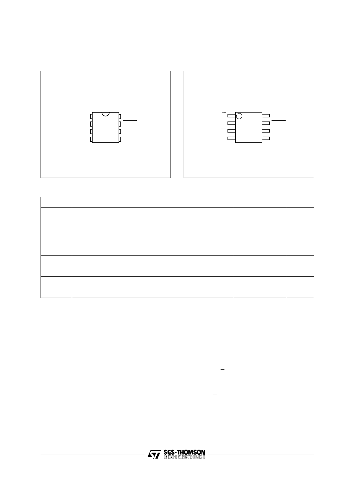
Figure 2A. DIP Pin Connect io ns
ST95P02
1
SV
2
3
W
4
SS
T ab le 2. Absolut e Maximu m Ra t ings
Symbol Parameter Value Unit
Ambient Operating Temperature –40 to 85 °C
Storage Temperature –65 to 150 °C
Lead Temperature, Soldering (SO8 package)
T
T
T
A
STG
LEAD
8
7
6
5
AI01257
CC
HOLDQ
C
DV
(1)
(PSDIP8 package)
Figure 2B. SO Pin Connecti ons
ST95P02
1
SV
2
3
W
SS
40 sec
10 sec
4
8
7
6
5
AI01258B
215
260
CC
HOLDQ
C
DV
°C
V
O
V
V
CC
V
ESD
Notes: 1. Except for the rating "Operating Temperature Range", stresses above those listed in the Table "Absolute Maximum Ratings"
2. MIL-STD-883C, 3015.7 (100pF , 1500Ω)
3. EIAJ IC-121 (Condition C) (200pF, 0Ω)
SIGNALS DESCRIPTION
Seri al Outp ut (Q ). The output pin is used to trans-
fer data serially out of the ST 95P02. Data is shifte d
out on the falling edge of the serial clock.
Serial Input (D). The input pin is used to transfer
data serially into the device. It receives inst ructions,
addresses, and data to be written. Input is latched
on the rising edge of the serial clock.
Serial Clock (C). The serial clock provides the
timing of the serial interface. Instructions, addresses, or data present at the input pin are latc hed
Output Voltage –0.3 to VCC +0.6 V
Input Voltage –0.3 to 6.5 V
I
Supply Voltage –0.3 to 6.5 V
Electrostatic Discharge Voltage (Human Body model)
Electrostatic Discharge Voltage (Machine model)
may cause permanent damage to the device. These are stress ratings only and operation of the device at these or any other
conditions above those indicat ed in the Operati ng sections of this specific ati on is not implied. Expos ure to Absolut e Maximum
Rating conditions for extended periods may affect device rel i abi lity. Refer also to the SGS-THOMSON SURE Program and
other relevant q ual ity doc ument s.
(2)
(3)
4000 V
500 V
on the rising edge of the clock input, while data on
the Q pin changes after the falling edge of the clock
input.
Chip Select (
S). This input is used to select the
ST95P02. The chip is selected by a high to low
transition on the
S pin when C is at ’0’ state. At any
time, the chip is deselected by a low to high transition on the
S pin when C is at ’0 ’ state. As soon as
the chip is deselected, the Q pin is at high impedance state. This pin allows multiple ST95P02 to
share the same SPI bus. After power up, the chip
is at the deselect state. T ransitions of
S are ignored
when C is at ’1’ state.
2/16
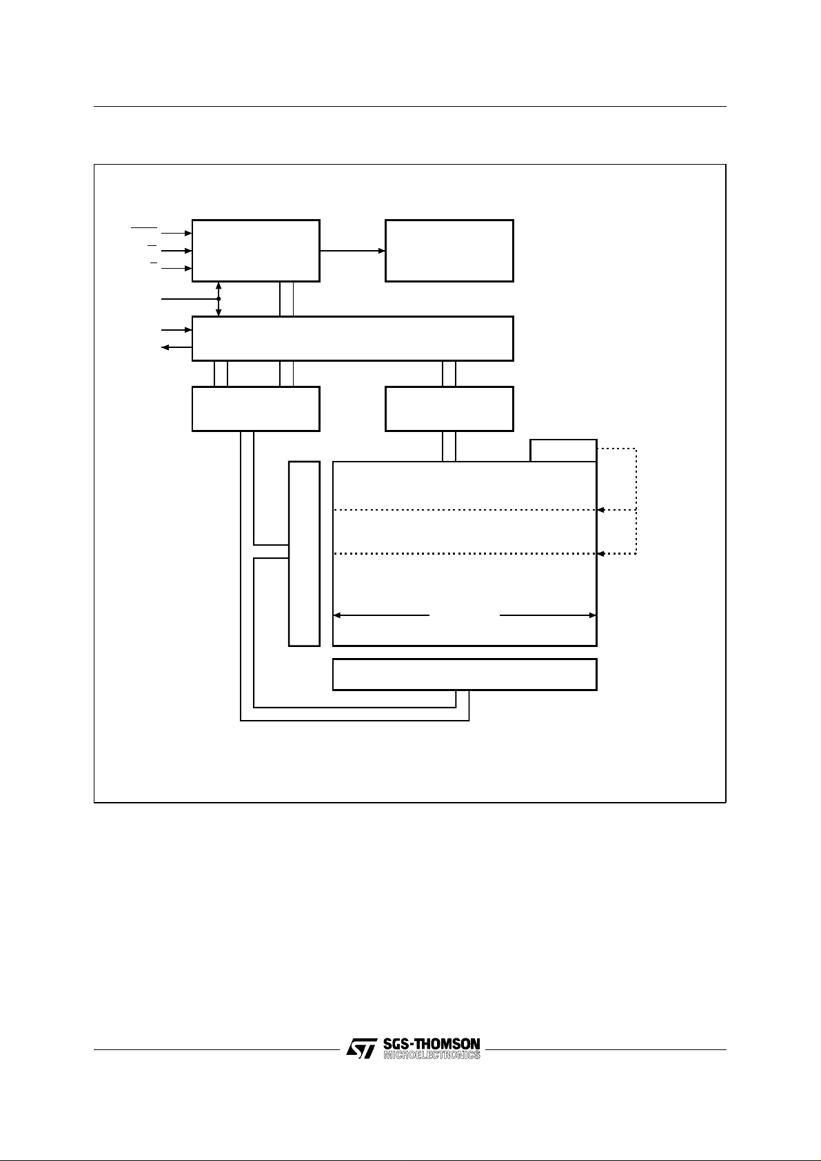
Figure 3. Block Diagram
ST95P02
HOLD
W
S
C
D
Q
Control Logic
I/O Shift Register
Address Register
and Counter
Y Decoder
High Voltage
Generator
Data
Register
Status
Block
Protect
16 Bytes
X Decoder
AI01272
3/16
ST95P02
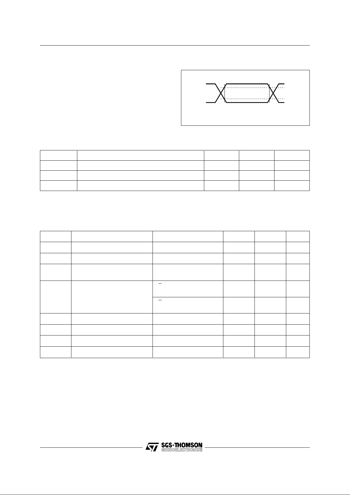
AC MEASUREMENT CONDITIONS
Figure 4. AC T estin g Input Ou tput W avefo r ms
Input Rise and Fall Times ≤ 50ns
Input Pulse Voltages 0.2V
Input and Output Timing
Reference Voltages
Note that Output Hi-Z is defined as the point where data
0.3V
to 0.8V
CC
to 0.7V
CC
CC
CC
0.8V
0.2V
CC
CC
is no longer driven.
T able 3. Input Parameters
(1)
(TA = 25 °C, f = 1 MHz )
Symbol Parameter Min Max Unit
C
IN
C
IN
t
LPF
Note: 1. Sampled only , not 100% test e d.
Input Capacitance (D) 8 pF
Input Capacitance (other pins) 6 pF
Input Signal Pulse Width 10 ns
T ab le 4. DC Characteristics
(T
= 0 to 70°C or –40 to 85°C; VCC = 3V to 5.5V)
A
0.7V
0.3V
AI00825
CC
CC
Symbol Parameter Test Condition Min Max Unit
I
LI
I
LO
I
CC
I
CC1
V
IL
V
IH
V
OL
V
OH
Input Leakage Current 2 µA
Output Leakage Current ±2 µA
VCC Supply Current (Active)
C = 0.1 V
@ 2 MHz, Q = Open
S = VCC, VIN = VSS or VCC,
VCC Supply Current (Standby)
S = VCC, VIN = VSS or VCC,
Input Low Voltage – 0.3 0.3 V
Input High Voltage 0.7 V
Output Low Voltage IOL = 2mA 0.2 V
Output High Voltage IOH = –2mA 0.8 V
V
V
= 5.5V
CC
CC
/0.9 VCC ,
CC
= 3V
CC
CC
2mA
50 µA
10 µA
CC
V
VCC + 1 V
CC
V
V
4/16

ST95P02
Table 5. AC Characteristics
= 0 to 70°C or –40 to 85°C; VCC = 3V to 5.5V)
(T
A
Symbol Alt Parameter Test Condition Min Max Unit
f
t
SLCH
t
CLSH
t
CH
t
t
CLCH
t
CHCL
t
DVCH
t
CHDX
t
DLDH
t
DHDL
t
HXCH
t
CLHX
t
SHSL
C
CL
t
t
t
t
t
t
t
DSU
t
t
t
HSU
t
t
f
SU
SH
WH
WL
RC
FC
DH
RI
t
FI
HH
CS
C
Clock Frequency D.C. 2 MHz
S Setup Time 50 ns
S Hold Time 50 ns
Clock High Time 200 ns
Clock Low Time 300 ns
Clock Rise Time 1 µs
Clock Fall Time 1 µs
Data In Setup Time 50 ns
Data In Hold Time 50 ns
Data In Rise Time 1 µs
Data In Fall Time 1 µs
HOLD Setup Time 50 ns
HOLD Hold Time 50 ns
S Deselect Time
4.5V < V
< 5.5V 200 ns
CC
3V < VCC < 4.5V 250 ns
t
SHQZ
t
QVCL
t
CLQX
t
QLQH
t
QHQL
t
HHQX
t
HLQZ
(1)
t
W
Note: 1. Not enough characterisation data were available on this parameter at the time of issue this Data Sheet. The typical value is well
t
DIS
t
V
t
HO
t
RO
t
FO
t
LZ
t
HZ
t
W
below 5ms, the maximum value will be reviewed and lowered when sufficient data is available.
Output Disable Time 150 ns
Clock Low to Output Valid 300 ns
Output Hold Time 0 ns
Output Rise Time 100 ns
Output Fall Time 100 ns
HOLD High to Output Low-Z 150 ns
HOLD Low to Output High-Z 150 ns
Write Cycle Time 10 ms
5/16
 Loading...