

2 Kbit Serial SPI EEPROM with High Speed Clock
HIGH SPEED CLOCK RATE:
– 2.1 MHz Max
1,000,000 ERASE/WRITE CYCLES
40 YEARS DA TA RETE NT ION
SINGLE 4.5V to 5.5V SUPPLY VOLTAGE
SPI BUS COMPATIBLE SERIAL INTERFACE
BLOCK WRITE PROTECTION
STATUS REGISTER
16 BYTE PAGE MODE
WRITE PROTECT
SELF-TIMED PROGRAMMING CY CLE
E.S.D.PROTECTION GREATER than 4000V
SUPPO RTS POSITIVE CLOCK SPI MODES
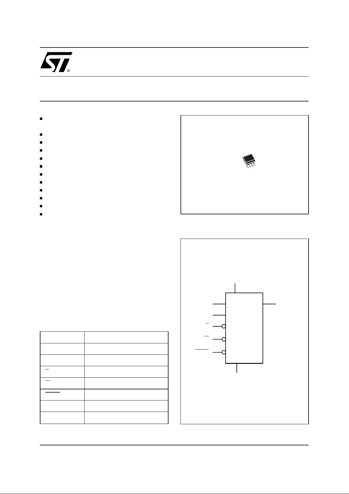
ST95022
8
1
SO8 (M)
150mil Width
Figure 1. Logic Diagram
DESCRIPTION
The ST95022 is an high speed 2 Kbit Electrically
Erasable Programmable Memory (EEPROM) fabricated with STMicroelectronics’s High Endurance
Single Polysilicon CMOS technology. The memory
is accessed by a simple SPI bus compatible serial
interface. The bus signals are a serial clock input
(C), a serial data input (D) and a serial data output
(Q).
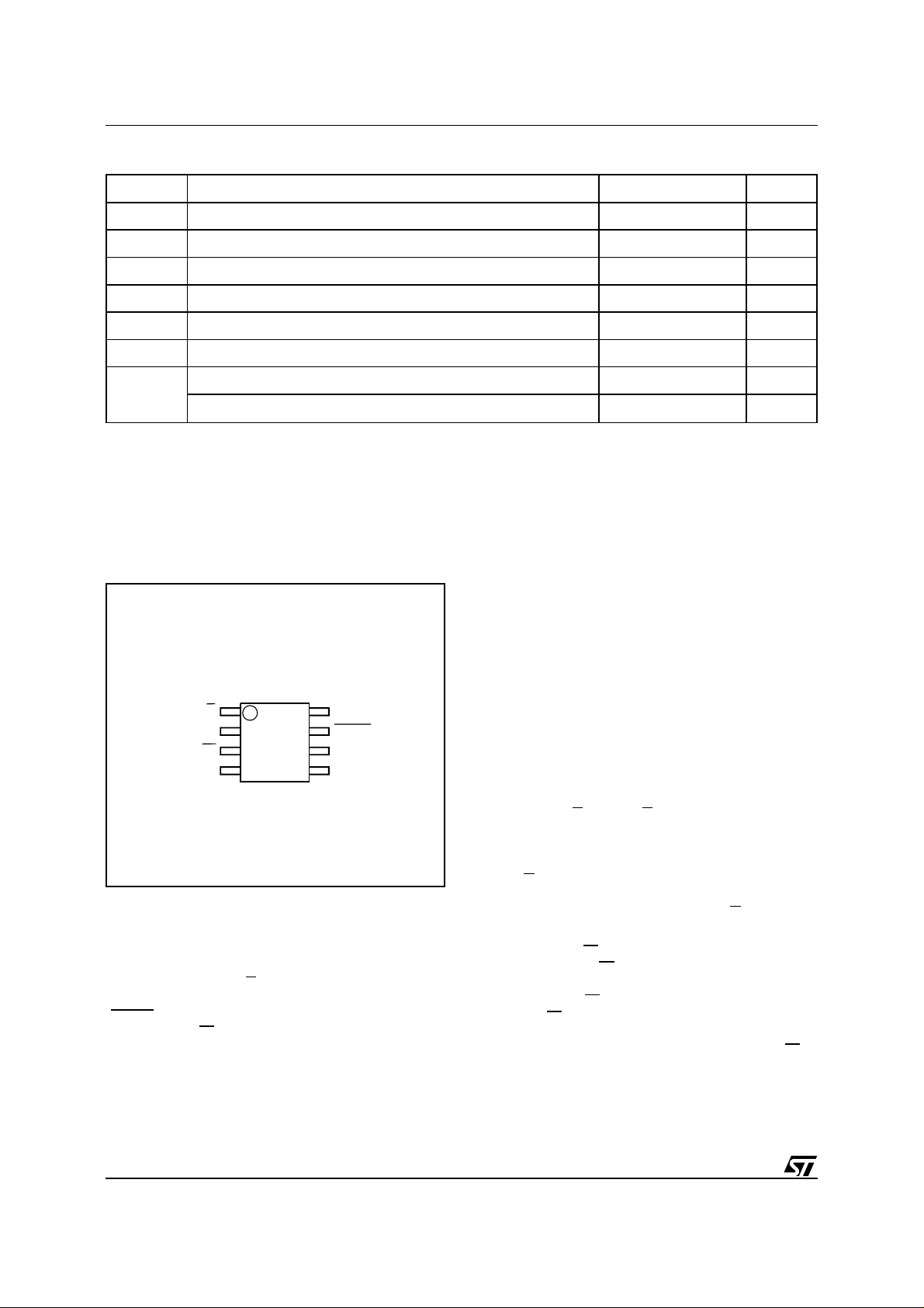
T ab le 1. Signal Names
C Serial Clock
D Serial Data Input
Q Serial Data Output
S Chip Select
W Write Protect
HOLD Hold
V
CC
Supply Voltage
W
HOLD
V
CC
D
C
S
ST95022
V
SS
Q
AI01722
V
SS
February 1999 1/16
Ground
ST95022
T ab le 2. Absolute Maximum Ratings
Symbol Parameter Value Unit
T
A
T
STG
T
LEAD
V
O
V
V
CC
V
ESD
Notes:
1. Except for the rating "Operating T emperature Range", stresses above those listed in the Table "Absolute Maximum Ratings"
2. Depends on range.
3. MIL-STD-883C, 3015.7 (100pF, 1500Ω)
4. EIAJ IC-121 (Condition C) (200pF , 0Ω)
Ambient Operating Temperature
Storage Temperature –65 to 150 °C
Lead Temperature, Soldering (SO8 package) 40 sec 215 °C
Output Voltage –0.3 to VCC +0.6 V
Input Voltage with respect to Ground –0.3 to 6.5 V
I
Supply Voltage –0.3 to 6.5 V
Electrostatic Discharge Voltage (Human Body model)
Electrostatic Discharge Voltage (Machine model)
may cause permanent damage to the device. These are stress rating s only and operation of the device at these or any other
conditions above those indicated in the Operating sections of this specification is not implied. Exposure to Absolute Maximum
Rating conditions for extended periods may affect device reliability. Refer also to the STMicroelectronics SURE Program and
other relevant quality documents.
Figure 2B. SO Pin Connections
(1)
(2)
(3)
(4)
–40 to 125 °C
4000 V
500 V
SIGNALS DESCRIPTION
Serial Output (Q).
The output pin is used to transfer data serially out of the ST95022. Data is shifted
out on the falling edge of the serial clock.
Serial Input (D).
The input pin is used to transfer
data serially into the device. It r eceives instructions,
ST95022
1
SV
2
3
W
SS
4
8
7
6
5
AI01723
CC
HOLDQ
C
DV
addresses, and the data to be written. Input is
latched on the rising edge of the serial clock.
Serial Clock (C).
The serial clock provides the
timing of the serial interface. Instructions, addresses, or data present at the input pin are latched
on the rising edge of the clock input, while data on
the Q pin changes after the falling edge of the clock
input.
Chip Select (
S).
When
S is high, the ST95022 is
deselected and the D output pin is at high impedance and, unless an internal write operation is
underway the ST95022 will be in the standby power
S low enables the ST95022, placing it in the
mode.
active power mode. It should be noted that af ter
S is required
DESCRIPTION
(cont’d)
The device connected to the bus is selected when
the chip select input (
S) goes low. Communications
with the chip can be interrupted with a hold input
HOLD). The write operation is disabled by a write
(
protect input (
W).
Data is clocked in during the low to high transition
of clock C, data is clocked out during the high to
low transition of clock C.
power-on, a high to low transition on
prior to the start of any operation.
Write Protect (
protection. When
W).
This pin is for hardware write
W is low, writes to the ST95022
memory are disabled but any other operations stay
enabled. When
available.
W is high, all writes operations are
W going low at any time before the last
bit D0 of the data stream will reset the write enable
latch and prevent programming. No action on
on the write enable latch can interrupt a write cycle
which has commenced.
W or
2/16
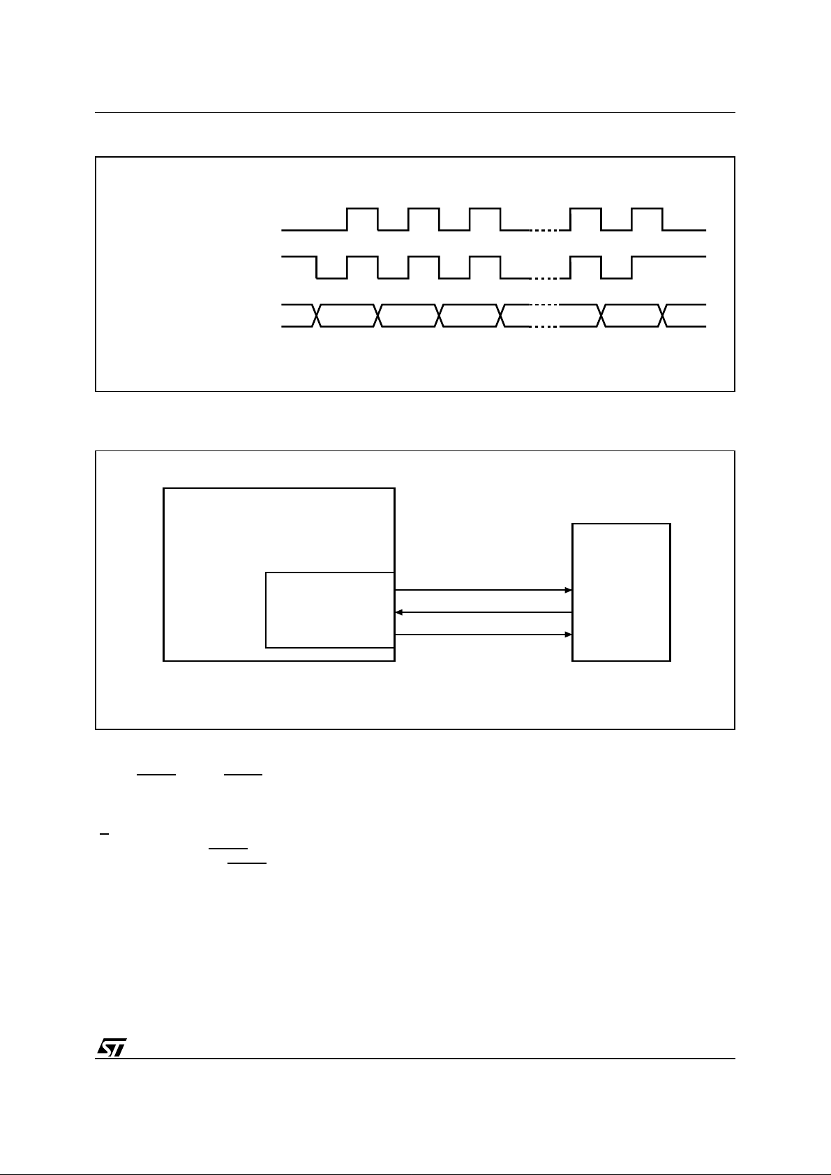
Figure 3. Data and Clock Timing
ST95022
CPOL
CPHA
0
1
0
1
C
C
D or Q
MSB LSB
Figure 4. Microcontroller and SPI Interface Set-up
MICROCONTROLLER
(ST6, ST7, ST9)
SPI Interface with
(CPOL, CPHA) =
('0', '0') or ('1', '1')
SCK
SDI
SDO
C
Q
D
AI01438
ST95xx0
HOLD ).
Hold (
HOLD pin is used to pause
The
serial communications with a ST95022 without resetting the serial sequence. To take the Hold condition into account, the product must be selected
(
S = 0). Then the Hold state is validated by a high
to low transition on
the communications,
HOLD when C is low . T o r esume
HOLD is brought high while
C is low. During the Hold condition D, Q , and C are
at a high impedance state.
When the ST95022 is under the Hold condition, it
is possible to deselect the device. However, the
serial communications will remain paused after a
reselect, and the chip will be reset.
AI01439
The ST95022 can be driven by a microcontroller
with its SPI peripheral running in either of the two
following modes: (CPOL, CPHA) = (’0’, ’0’) or
(CPOL, CPHA) = (’1’, ’1’).
For these two modes, input data is latched in by the
low to high transition of clock C, and output data is
available from the high to low transition of Clock
(C).
The difference between (CPOL, CPHA) = (0, 0) and
(CPOL, CPHA) = (1, 1) is the stand-by polarity: C
remains at ’0’ for (CPOL, CPHA) = (0, 0) and C
remains at ’1’ for (CPOL, CPHA) = ( 1, 1) when there
is no data transfer.
3/16

ST95022
OPERATIONS
All instructions, addresses and data are shifted in
and out of the chip MSB first. Data input (D) is
sampled on the first rising edge of clock (C) after
the chip select (
S) goes low. Prior to any operation,
a one-byte instruction code must be entered in the
chip. This code is entered via the data input (D),
and latched on the rising edge of the clock input
(C). T o enter an instruction code, the product must
have been previously selected (
S = low). Table 3
shows the instruction set and format for device
operation. If an invalid instruction is sent (one not
contained in Table 3), the chip is automatically
deselected.
Write Enable (WREN) and Write Disable (WR DI)
The ST95022 contains a write enable latch. This
latch must be set prior to every WRITE or WRSR
operation. The WREN instruction will set the latch
and the WRDI instruction will reset the latch. The
latch is reset under the following conditions:
W pin is low
–
– Power on
– WRDI instruction executed
– WRSR instruction executed
– WRITE instruction executed
As soon as the WREN or WRDI instruction is
received by the ST95022, the circuit executes the
instruction and enters a wait mode until it is deselected.
Read Status Register (RDSR)
The RDSR instruction provides access to the status
register. The status register may be read at any
time, even during a write to the memory operation.
As soon as the 8th bit of the status register is read
out, the ST95022 enters a wait mode (data on D is
not decoded, Q is in Hi-Z) until it is deselected.
The status register format is as follows:
b7 b0
1 1 1 1 BP1 BP0 WEL WIP
BP1, BP0: Read and write bits.
WEL, WIP: Read only bits.
b7 to b4: Read only bits.
During a write to the memory operation to the
memory array, all bits BP1, BP0, WEL, WIP are
valid and can be read. During a write to the status
register, only the bits WEL and WIP are valid and
can be read. The values of BP1 and BP0 read at
that time correspond to the previous contents of the
status register.
The Write-In-Process (WIP) read-only bit indicates
whether the ST95022 is busy with a write operation. When set to a ’1’ a write is in progress, when
set to a ’0’ no write is in progress.
The Write Enable Latch (WEL) read-only bit indicates the status of the write enable latch. When set
to a ’1’ the lat ch is set, when set t o a ’0’ the latch is
reset. The Block Protect (BP0 and BP1) bits indicate the extent of the protection employed. These
bits are set by the user issuing the WRSR instruction. These bits are non-volatile.
Write Status Register (WRSR)
The WRSR instruction allows the user to select the
size of protected memory. The ST95022 is divided
into four 512 bit blocks. The user may read the
blocks but will be unable to write within the pro-
T ab le 3. Instruction Set
Instruction Description Instruction Format
WREN Set Write Enable Latch 0000 0110
WRDI Reset Write Enable Latch 0000 0100
RDSR Read Status Register 0000 0101
WRSR Write Status Register 0000 0001
READ Read Data from Memory Array 0000 0011
WRITE Write Data to Memory Array 0000 0010
Notes:
A = 1, Upper page selected
A = 0, Lower page selected
4/16
Figure 5. Block Diagram
ST95022
HOLD
W
S
C
D
Q
Control Logic
I/O Shift Register
Address Register
and Counter
Y Decoder
High Voltage
Generator
Data
Register
Status
Block
Protect
16 Bytes
tected blocks. The blocks and respective WRSR
control bits are shown in Table 4.
When the WRSR instruction and the 8 bits of the
Status Register are latched-in, the internal write
cycle is then triggered by the ris ing edge of
This rising edge of
S must appear no later than the
S.
16th clock cycle of the WRSR instruction of the
Status Register content (it must not appear a 17th
clock pulse before the rising edge of
S), otherwise
the internal write sequence is not performed.
X Decoder
T ab le 4. Write Protected Block Size
Status Register
Bits
BP1 BP0
0 0 none none
0 1 C0h - FFh Upper quarter
1 0 80h - FFh Upper half
1 1 00h - FFh Whole memory
Array
Addresses
Protected
Protected
AI01272
Block
5/16
 Loading...