

SGS Thomson Microelectronics ST93CS67, ST93CS66 Datasheet

4K (256 x 16) SERIAL MICROWIRE EEPROM
1 MILLIONERASE/WRITE CYCLES, with
40 YEARS DATARETENTION
SELF-TIMED PROGRAMMINGCYCLE with
AUTO-ERASE
READY/BUSYSIGNALDURING
PROGRAMMING
SINGLESUPPLYVOLTAGE
– 3V to 5.5V for the ST93CS66
– 2.5V to 5.5V for the ST93CS67
USER DEFINEDWRITE PROTECTED AREA
PAGEWRITE MODE (4 WORDS)
SEQUENTIALREAD OPERATION
5ms TYPICALPROGRAMMINGTIME
ST93CS66and ST93CS67 are replaced by
the M93S66
8
1
PSDIP8 (B)
0.25mm Frame
Figure 1. Logic Diagram
ST93CS66
ST93CS67
NOT FOR NEW DESIGN
14
1
SO14 (ML)
150mil Width
DESCRIPTION
The ST93CS66 and ST93CS67 are 4K bit ElectricallyErasable ProgrammableMemory(EEPROM)
fabricatedwithSGS-THOMSON’sHighEndurance
SinglePolysiliconCMOStechnology.The memory
is accessed through a serial inputD and outputQ.
The 4K bit memory is organized as 256 x 16 bit
words.Thememory is accessedby aset of instructionswhich include Read, Write, Page Write, Write
Allandinstructionsused to set thememoryprotection. A Read instruction loads the address of the
first word to be read into an internal address
pointer.
Table 1. Signal Names
S Chip Select Input
D Serial Data Input
Q Serial Data Output
C Serial Clock
PRE Protect Enable
W Write Enable
V
CC
V
SS
Supply Voltage
Ground
V
CC
D
CQ
S
PRE
W
ST93CS66
ST93CS67
V
SS
AI00906B
June 1997 1/16
This isinformation on a productstill in productionbutnot recommendedfor new designs.

ST93CS66,ST93CS67
Figure 2A. DIP Pin Connections
Figure2B. SO PinConnections
ST93CS66
ST93CS67
ST93CS66
ST93CS67
SV
1
2
D
3
Q
4
Table 2. Absolute Maximum Ratings
Symbol Parameter Value Unit
T
T
STG
T
LEAD
V
V
CC
V
ESD
Notes: 1. Exceptfor the rating ”Operating Temperature Range”, stresses above those listed in the Table ”Absolute Maximum Ratings”
Ambient Operating Temperature –40 to85 °C
A
Storage Temperature –65 to150 °C
Lead Temperature,Soldering (SO14 package)
Input or Output Voltages(Q = VOHor Hi-Z) –0.3 to VCC+0.5 V
IO
Supply Voltage –0.3 to 6.5 V
Electrostatic Discharge Voltage (Human Body model)
Electrostatic Discharge Voltage (Machine model)
may cause permanent damage to the device. These are stressratings only and operation of thedevice at these or any other
conditions abovethose indicated in the Operating sections of this specification is not implied. Exposure toAbsolute Maximum
Rating conditions for extended periods may affect device reliability.Refer also to the SGS-THOMSON SURE Program and other
relevant quality documents.
2. MIL-STD-883C, 3015.7(100pF, 1500 Ω).
3. EIAJ IC-121 (Condition C) (200pF, 0 Ω).
8
7
6
5
AI00907B
PREC
W
V
CC
SS
Warning: NC = Not Connected.
(1)
(PSDIP8 package)
(2)
(3)
NC
NC
40 sec
10 sec
1
14
NC
2
S
3
C
4
DW
5
QV
6
7
AI00908C
V
13
12
11
CC
PRE
NC
10
9
SS
8NCNC
215
260
2000 V
500 V
°C
DESCRIPTION (cont’d)
The data is then clocked out serially. The address
pointer is automaticallyincremented after the data
is output and, if the Chip Select input (S) is held
High, the ST93CS66/67 can output a sequential
streamof data words. In thisway,thememory can
be read as a data stream of 16 to 4096 bits, or
continuouslyas the addresscounterautomatically
rolls over to 00 when the highest address is
reached.
Within the time required by a programming cycle
(t
), up to 4 wordsmay be written with the help of
W
the Page Write instruction;thewhole memorymay
alsobe erased,or set to a predetermined pattern,
by using the WriteAll instruction.
Within the memory, an user defined area may be
protected against further Write instructions. The
2/16
size of this area is defined by the content of a
Protect Register, located outside of the memory
array. As a final protection step, data may be permanently protected by programming a One Time
Programing bit (OTP bit) which locks the Protect
Registercontent.
Programming is internally self-timed (the external
clocksignal on Cinput may be disconnectedorleft
running after the start of a Write cycle) and does
notrequirean erasecyclepriorto the Writeinstruction.TheWriteinstructionwrites 16bits at onetime
intoone of the 256 words, the PageWrite instruction writes up to 4 words of 16 bits to sequential
locations, assuming in both cases that all addressesareoutsidetheWrite Protectedarea. After
the start of the programming cycle, a Ready/Busy
signalis availableon the Data output(Q) when the
ChipSelect (S)input pin is driven High.

ST93CS66, ST93CS67
AC MEASUREMENT CONDITIONS
Figure 3. ACTesting Input Output Waveforms
Input Rise and Fall Times ≤ 20ns
0.8V
0.2V
CC
CC
0.7V
0.3V
AI00825
0.3V
CC
CC
to 0.8V
to 0.7V
CC
CC
Input Pulse Voltages 0.2V
Input and Output Timing
Reference Voltages
Note that Output Hi-Z is defined as the point where data
is no longer driven.
Table 3. Capacitance
(1)
(TA=25°C, f =1 MHz)
Symbol Parameter Test Condition Min Max Unit
C
IN
C
OUT
Note: 1. Sampled only, not 100% tested.
Input Capacitance VIN=0V 5 pF
Output Capacitance V
=0V 5 pF
OUT
Table 4. DC Characteristics(TA= 0 to 70°C or –40 to 85°C; VCC=3V to 5.5V for ST93CS66 and
= 2.5Vto 5.5V for ST93CS67)
V
CC
Symbol Parameter TestCondition Min Max Unit
I
I
I
CC1
V
V
V
V
I
LI
LO
CC
IL
IH
OL
OH
Input Leakage Current 0V ≤ VIN≤ V
Output Leakage Current
0V ≤ V
≤ VCC,
OUT
Q inHi-Z
CC
±2.5 µA
±2.5 µA
Supply Current (TTL Inputs) S = VIH, f = 1 MHz 3 mA
Supply Current (CMOS Inputs) S = V
Supply Current (Standby) S = VSS,C=V
, f = 1 MHz 2 mA
IH
SS
50 µA
Input Low Voltage (ST93CS66,67) 4.5V ≤ VCC≤ 5.5V –0.1 0.8 V
Input Low Voltage (ST93CS66) 3V ≤ V
Input Low Voltage (ST93CS67) 2.5V ≤ V
≤ 5.5V –0.1 0.2 V
CC
≤ 5.5V –0.1 0.2 V
CC
CC
CC
Input High Voltage (ST93CS66,67) 4.5V ≤ VCC≤ 5.5V 2 VCC+1 V
Input High Voltage (ST93CS66) 3V ≤ V
Input High Voltage (ST93CS67) 2.5V ≤ V
Output Low Voltage
Output High Voltage
I
≤ 5.5V 0.8 V
CC
≤ 5.5V 0.8 V
CC
I
= 2.1mA 0.4 V
OL
I
=10µA 0.2 V
OL
= –400µA 2.4 V
OH
I
= –10µAV
OH
CC
CC
–0.2 V
CC
VCC+1 V
VCC+1 V
CC
CC
V
V
3/16
ST93CS66,ST93CS67
Table 5. ACCharacteristics (TA=0 to70° or,–40 to 85°C; VCC= 3V to 5.5V for ST93CS66 and
V
= 2.5Vto 5.5V for ST93CS67)
CC
Symbol Alt Parameter Test Condition Min Max Unit
t
PRVCH
t
WVCH
t
SHCH
t
DVCH
t
CHDX
t
CHQL
t
CHQV
t
CLPRX
t
SLWX
t
CLSL
t
SLSH
t
SHQV
t
SLQZ
t
CHCL
t
CLCH
t
W
f
C
Notes: 1. Chip Select must be brought low for a minimum of 250 ns (t
2. The Clock frequency specification calls for a minimum clockperiod of 1 µs, therefore the sum of the timings t
t
PRES
t
PES
t
CSS
t
DIS
t
DIH
t
PD0
t
PD1
t
PREH
t
PEH
t
CSH
t
CS
t
SV
t
DF
t
SKH
t
SKL
t
WP
f
SK
must be greater or equal to 1 µs. For example, ift
Protect Enable Valid to Clock High 50 ns
Write Enable Validto Clock High 50 ns
Chip Select High to Clock High 50 ns
Input Valid to Clock High 100 ns
Clock High to Input Transition 100 ns
Clock High to Output Low 500 ns
Clock High to Output Valid 500 ns
Clock Low to Protect Enable Transition 0 ns
Chip Select Low to Write Enable Transition 250 ns
Clock Low to Chip Select Transition 0 ns
Chip Select Low to Chip Select High Note 1 250 ns
Chip Select High to Output Valid 500 ns
Chip Select Low to Output Hi-Z 300 ns
Clock High to Clock Low Note 2 250 ns
Clock Low to Clock High Note 2 250 ns
Erase/Write Cycle time 10 ms
Clock Frequency 0 1 MHz
) betweenconsecutive instructioncycles.
is 250 ns, then t
CHCL
SLSH
must be at least 750ns.
CLCH
CHCL+tCLCH
Figure4. Synchronous Timing,Start and Op-Code Input
PRE
tPRVCH
W
C
tSHCH tCLCH
S
D
START
4/16
OP CODE OP CODESTART
OP CODE INPUT
tCHCLtWVCH
tCHDXtDVCH
AI00887

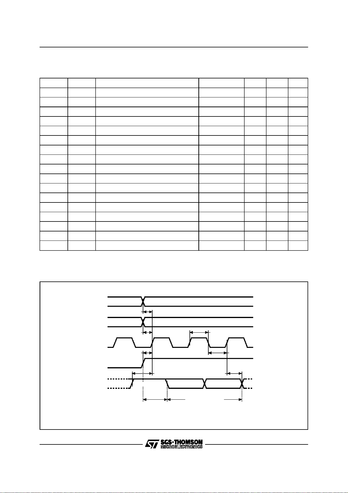
Figure5. Synchronous Timing,Read or Write
C
S
ST93CS66, ST93CS67
tCLSL
D
Q
PRE
W
C
S
Hi-Z
tDVCH
An
ADDRESS INPUT
tCHQL
A0
tCHQVtCHDX
tSLQZ
Q15/Q7 Q0
DATA OUTPUT
tCLPRX
tSLWX
tCLSL
tSLSH
tSLSH
AI00820C
tDVCH
D
Q
An A0/D0
Hi-Z
tCHDX
tSHQV
BUSY
tW
WRITE CYCLEADDRESS/DATA INPUT
tSLQZ
READY
AI00888B
5/16
 Loading...