

SGS Thomson Microelectronics ST93CS46, ST93CS47 Datasheet
1K (64 x 16) SERIAL MICROWIREEEPROM
1 MILLION ERASE/WRITECYCLES,with
40 YEARS DATARETENTION
SELF-TIMED PROGRAMMINGCYCLE with
AUTO-ERASE
READY/BUSYSIGNALDURING
PROGRAMMING
SINGLESUPPLYVOLTAGE
– 3V to 5.5V for the ST93CS46
– 2.5V to 5.5V for the ST93CS47
USER DEFINEDWRITE PROTECTED AREA
PAGEWRITE MODE (4 WORDS)
SEQUENTIAL READ OPERATION
5ms TYPICALPROGRAMMING TIME
ST93CS46andST93CS47are replaced by
the M93S46
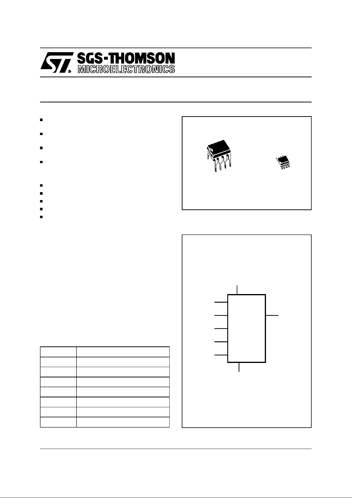
8
1
PSDIP8 (B)
0.4mm Frame
Figure 1. Logic Diagram
ST93CS46
ST93CS47
NOT FOR NEW DESIGN
8
1
SO8 (M)
150mil Width
DESCRIPTION
The ST93CS46 and ST93CS47 are 1K bit ElectricallyErasable ProgrammableMemory (EEPROM)
fabricatedwithSGS-THOMSON’sHigh Endurance
SinglePolysiliconCMOStechnology.Thememory
is accessedthrough a serial input D and output Q.
The 1K bit memory is organized as 64 x 16 bit
words.Thememory is accessedbyasetofinstructionswhich includeRead,Write, Page Write, Write
Allandinstructionsusedtosetthememoryprotection. A Read instruction loads the address of the
first word to be read into an internal address
pointer.
Table 1. Signal Names
S Chip Select Input
D Serial Data Input
Q Serial Data Output
C Serial Clock
PRE Protect Enable
W Write Enable
V
CC
V
SS
Supply Voltage
Ground
V
CC
D
CQ
S
PRE
W
ST93CS46
ST93CS47
V
SS
AI00884B
June 1997 1/16
This isinformation on a product still inproduction but not recommended for new designs.
ST93CS46,ST93CS47
Figure2A. DIPPin Connections
ST93CS46
ST93CS47
SV
1
2
D
3
Q
4
Table 2. Absolute Maximum Ratings
Symbol Parameter Value Unit
T
T
STG
T
LEAD
V
V
CC
V
ESD
Notes: 1. Except for the rating ”Operating Temperature Range”, stresses above those listed in the Table ”Absolute Maximum Ratings”
Ambient Operating Temperature –40 to85 °C
A
Storage Temperature –65 to150 °C
Lead Temperature,Soldering (SO8 package)
Input or Output Voltages (Q = VOHor Hi-Z) –0.3 to VCC+0.5 V
IO
Supply Voltage –0.3 to 6.5 V
Electrostatic Discharge Voltage(Human Body model)
Electrostatic Discharge Voltage(Machine model)
may cause permanent damage to the device. These are stress ratings only and operationof thedeviceat these or any other
conditions above those indicated in the Operating sectionsof this specification is not implied.Exposure toAbsolute Maximum
Rating conditions for extendedperiods may affect device reliability.Refer also to the SGS-THOMSON SURE Program and other
relevant quality documents.
2. MIL-STD-883C, 3015.7(100pF, 1500 Ω).
3. EIAJ IC-121 (ConditionC) (200pF, 0Ω).
8
7
6
5
AI00885B
PREC
W
V
CC
SS
(1)
(PSDIP8 package)
Figure2B. SOPin Connections
ST93CS46
ST93CS47
1
SV
2
D
3
Q
4
40 sec
10 sec
(2)
(3)
8
7
6
5
AI00886C
215
260
3000 V
500 V
PREC
W
V
CC
SS
°C
DESCRIPTION (cont’d)
The data is then clocked out serially. The address
pointer is automaticallyincremented after the data
is output and, if the Chip Select input (S) is held
High, the ST93CS46/47 can output a sequential
streamof data words. In this way,thememory can
be read as a data stream of 16 to 1024 bits, or
continuouslyas the addresscounterautomatically
rolls over to 00 when the highest address is
reached. Within the time required by a programmingcycle(t
), upto 4 wordsmay be written with
W
the help of the Page Write instruction; the whole
memorymay also be erased, or set to a predeterminedpattern, by using the Write All instruction.
Within the memory, an user defined area may be
protected against further Write instructions. The
size of this area is defined by the content of a
2/16
Protect Register, located outside of the memory
array. As a final protection step, data may be permanently protected by programming a One Time
Programing bit (OTP bit) which locks the Protect
Registercontent.
Programming is internally self-timed (the external
clocksignal on Cinput maybedisconnectedor left
running after the start of a Write cycle) and does
notrequirean erasecycle priortotheWriteinstruction.TheWriteinstructionwrites16bits at onetime
intooneofthe64words,thePageWriteinstruction
writesup to 4 words of 16 bits to sequentiallocations, assuming in both cases that all addresses
are outside the Write Protectedarea.
After t he start of the programming cycle, a
Ready/Busysignal is available on the Data output
(Q) when the Chip Select (S) input pin is driven
High.
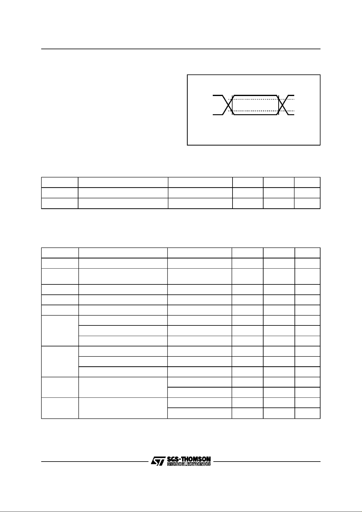
AC MEASUREMENT CONDITIONS
Input Rise and Fall Times ≤ 20ns(10% to 90%)
Input Pulse Voltages 0.4V to 2.4V
Input and Output Timing
Reference Voltages
Note that Output Hi-Z is defined as the point where data
is no longer driven.
0.8 and 2V
ST93CS46, ST93CS47
Figure 3. AC TestingInputOutput Waveforms
0.8V
0.2V
CC
CC
0.7V
0.3V
AI00825
CC
CC
Table 3. Capacitance
(1)
(TA=25°C, f = 1 MHz )
Symbol Parameter Test Condition Min Max Unit
C
IN
C
OUT
Note: 1. Sampled only, not 100%tested.
Input Capacitance VIN=0V 5 pF
Output Capacitance V
=0V 5 pF
OUT
Table 4. DC Characteristics(TA= 0 to 70°C or –40 to 85°C; VCC=3V to 5.5V for ST93CS46 and
= 2.5Vto 5.5V for ST93CS47)
V
CC
Symbol Parameter TestCondition Min Max Unit
I
I
I
CC1
V
V
V
V
I
LI
LO
CC
IL
IH
OL
OH
Input Leakage Current 0V ≤ VIN≤ V
Output LeakageCurrent
0V ≤ V
≤ VCC,
OUT
Q in Hi-Z
CC
±2.5 µA
±2.5 µA
Supply Current (TTL Inputs) S = VIH, f = 1 MHz 3 mA
Supply Current (CMOS Inputs) S = V
Supply Current (Standby) S = VSS,C=V
, f = 1 MHz 2 mA
IH
SS
50 µA
Input Low Voltage (ST93CS46,47) 4.5V ≤ VCC≤ 5.5V –0.1 0.8 V
Input Low Voltage (ST93CS46) 3V ≤ V
Input Low Voltage (ST93CS47) 2.5V ≤ V
≤ 5.5V –0.1 0.2 V
CC
≤ 5.5V –0.1 0.2 V
CC
CC
CC
Input HighVoltage (ST93CS46,47) 4.5V ≤ VCC≤ 5.5V 2 VCC+1 V
Input HighVoltage (ST93CS46) 3V ≤ V
Input HighVoltage (ST93CS47) 2.5V ≤ V
Output Low Voltage
Output High Voltage
I
≤ 5.5V 0.8 V
CC
≤ 5.5V 0.8 V
CC
I
= 2.1mA 0.4 V
OL
I
=10µA 0.2 V
OL
= –400µA 2.4 V
OH
I
= –10µAV
OH
CC
CC
–0.2 V
CC
VCC+1 V
VCC+1 V
V
V
3/16
ST93CS46,ST93CS47
Table 5. DC Characteristics(TA= 0 to 70°C or –40 to 85°C; VCC=3V to 5.5V for ST93CS46 and
V
= 2.5Vto 5.5V for ST93CS47)
CC
Symbol Alt Parameter Test Condition Min Max Unit
t
PRVCH
t
WVCH
t
SHCH
t
DVCH
t
CHDX
t
CHQL
t
CHQV
t
CLPRX
t
SLWX
t
CLSL
t
SLSH
t
SHQV
t
SLQZ
t
CHCL
t
CLCH
t
W
f
C
Notes: 1. Chip Select must be brought low for a minimum of 250 ns (t
2. The Clock frequency specification calls for a minimum clockperiod of 1 µs, therefore the sumofthetimings t
t
PRES
t
PES
t
CSS
t
DIS
t
DIH
t
PD0
t
PD1
t
PREH
t
PEH
t
CSH
t
CS
t
SV
t
DF
t
SKH
t
SKL
t
WP
f
SK
must be greater or equal to 1 µs.For example, ift
Protect Enable Valid to Clock High 50 ns
Write Enable Valid to Clock High 50 ns
Chip Select High to Clock High 50 ns
Input Valid to Clock High 100 ns
Clock High to InputTransition 100 ns
Clock High to Output Low 500 ns
Clock High to Output Valid 500 ns
Clock Low to Protect Enable Transition 0 ns
Chip Select Low to Write Enable Transition 250 ns
Clock Low to Chip Select Transition 0 ns
Chip Select Low to Chip Select High Note 1 250 ns
Chip Select High to Output Valid 500 ns
Chip Select Low to Output Hi-Z 300 ns
Clock High to Clock Low Note 2 250 ns
Clock Low to Clock High Note 2 250 ns
Erase/Write Cycle time 10 ms
Clock Frequency 0 1 MHz
) between consecutive instruction cycles.
is 250 ns, then t
CHCL
SLSH
must be atleast 750 ns.
CLCH
CHCL+tCLCH
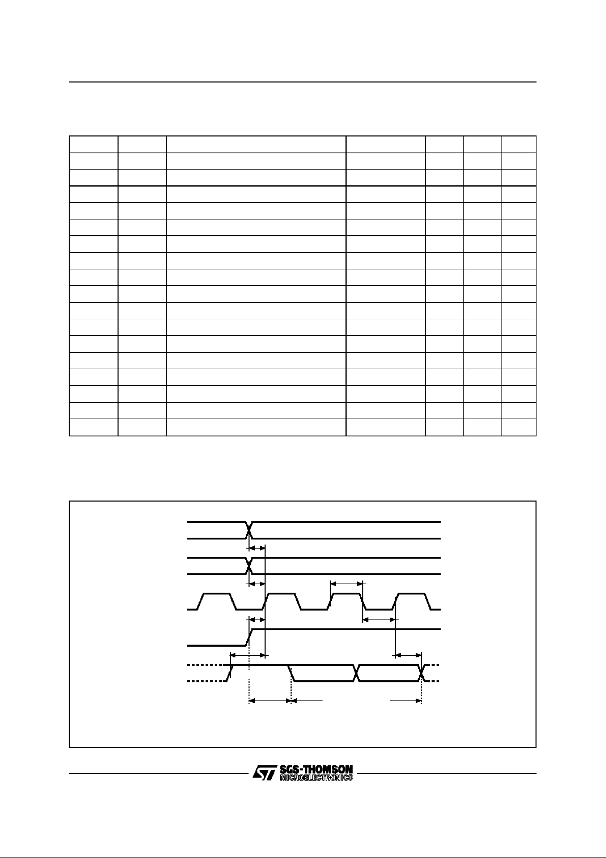
Figure4. Synchronous Timing, Start and Op-CodeInput
PRE
tPRVCH
W
C
tSHCH tCLCH
S
D
START
4/16
OP CODE OP CODESTART
OP CODE INPUT
tCHCLtWVCH
tCHDXtDVCH
AI00887

Figure5. Synchronous Timing,Read or Write
C
S
ST93CS46, ST93CS47
tCLSL
D
Q
PRE
W
C
S
Hi-Z
tDVCH
An
ADDRESS INPUT
tCHQL
A0
tCHQVtCHDX
tSLQZ
Q15/Q7 Q0
DATA OUTPUT
tCLPRX
tSLWX
tCLSL
tSLSH
tSLSH
AI00820C
tDVCH
D
Q
An A0/D0
Hi-Z
tCHDX
tSHQV
BUSY
tW
WRITE CYCLEADDRESS/DATA INPUT
tSLQZ
READY
AI00888B
5/16
 Loading...