


SGS Thomson Microelectronics ST779ACN, ST779ACD-TR, ST779ACD, ST778ACN, ST778ACD-TR Datasheet
...
1/11October 2002
■ 1V TO 6V INPUT GUARANTEES START-UP
UNDER LOAD
■ MAXIMUM OUTPUT CURRENT OF 300mA
(778OR 779 ADJUSTED TO 3V)
■ LOAD FULLY DISCONNECTEDIN
SHUTDOWN
■ TYPICAL EFFICIENCY OF 82%
■ INTERNAL 1A PO WER SWITCH AND
SYNCHRONOUS RECTIFIER
■ ADJUSTABLE CURRENT LIMIT ALLOWS
LOW-COST INDUCTORS
■ SUPPLY CURRENT OF 270µA (NO LOAD )
■ SHUTDOWN SUPPLY CURRENT 20µA
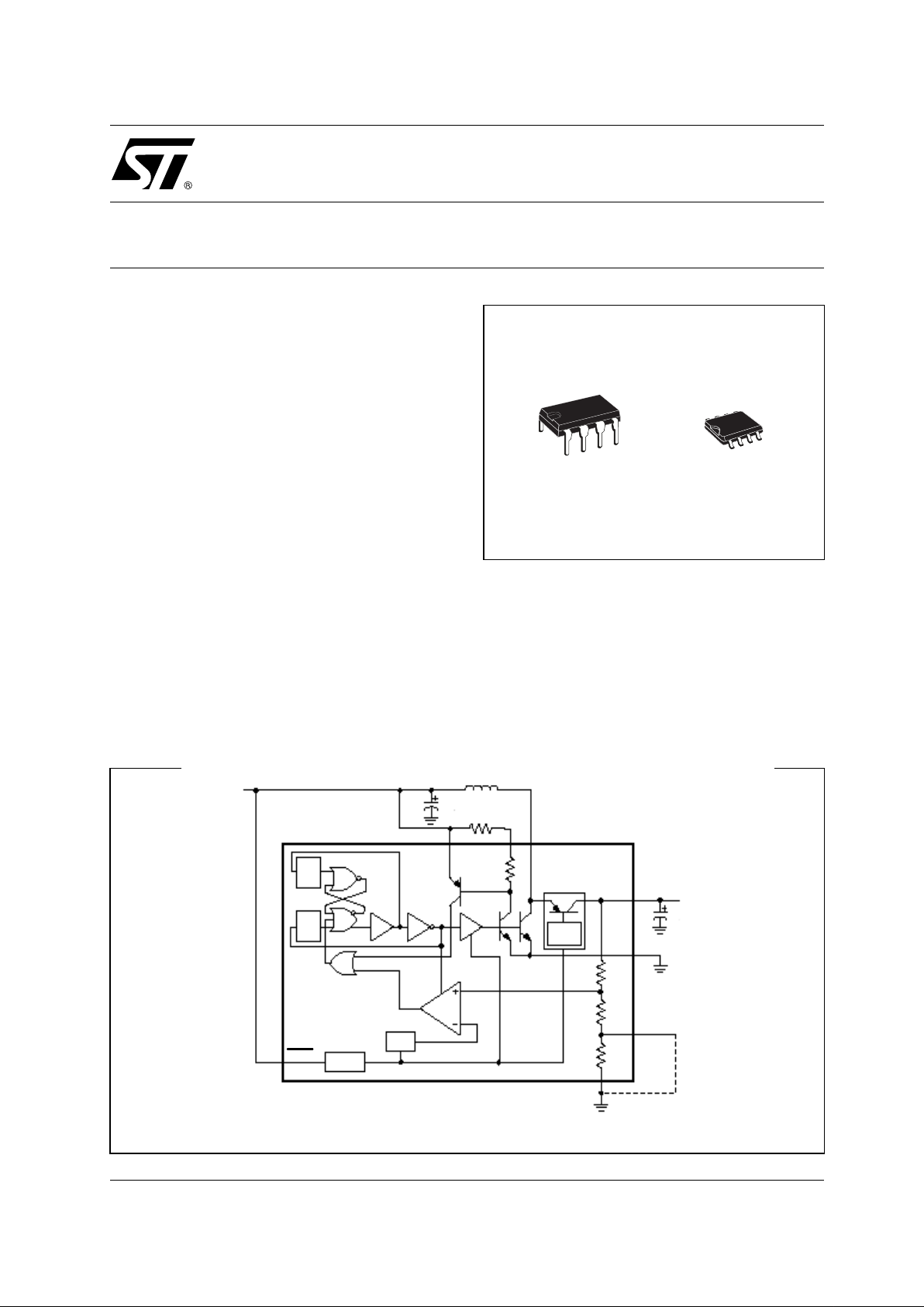
■ PACKAGE AVAILABLE: DIP-8 AND SO-8
DESCRIPTION
The ST777/778/779 are dc-dc converters that
step-up from low voltage inputs requiring only
three external components, an inductor (typically
22µH) and two capacitors. The device includ e a
Sinchronous Rectifier that elimina tes the need for
an external catch diode, and allows regulation
even when the input is greater than the output.
Unlike others step-up DC-DC converters the
ST777/778/779’s Sinchronous Rectifierturns off in
the shu tdown mode, fully disconnecting the output
from the source. This eliminates the current drain
associated with conventional step-up c onverters
when off or in shutdown. Supply current is 270µA
under no load and only 20µA in stand by mode.
ST777/778/779
LOW VOLTAG E INPUT, 3-3.3V/5V/ADJUSTABLE OUTPUT
DC-DC CONVERTER WITH SYNCHRONOUS RECTIFIER
V
IN
V
O
22µH
100µF
100µF
RLIM
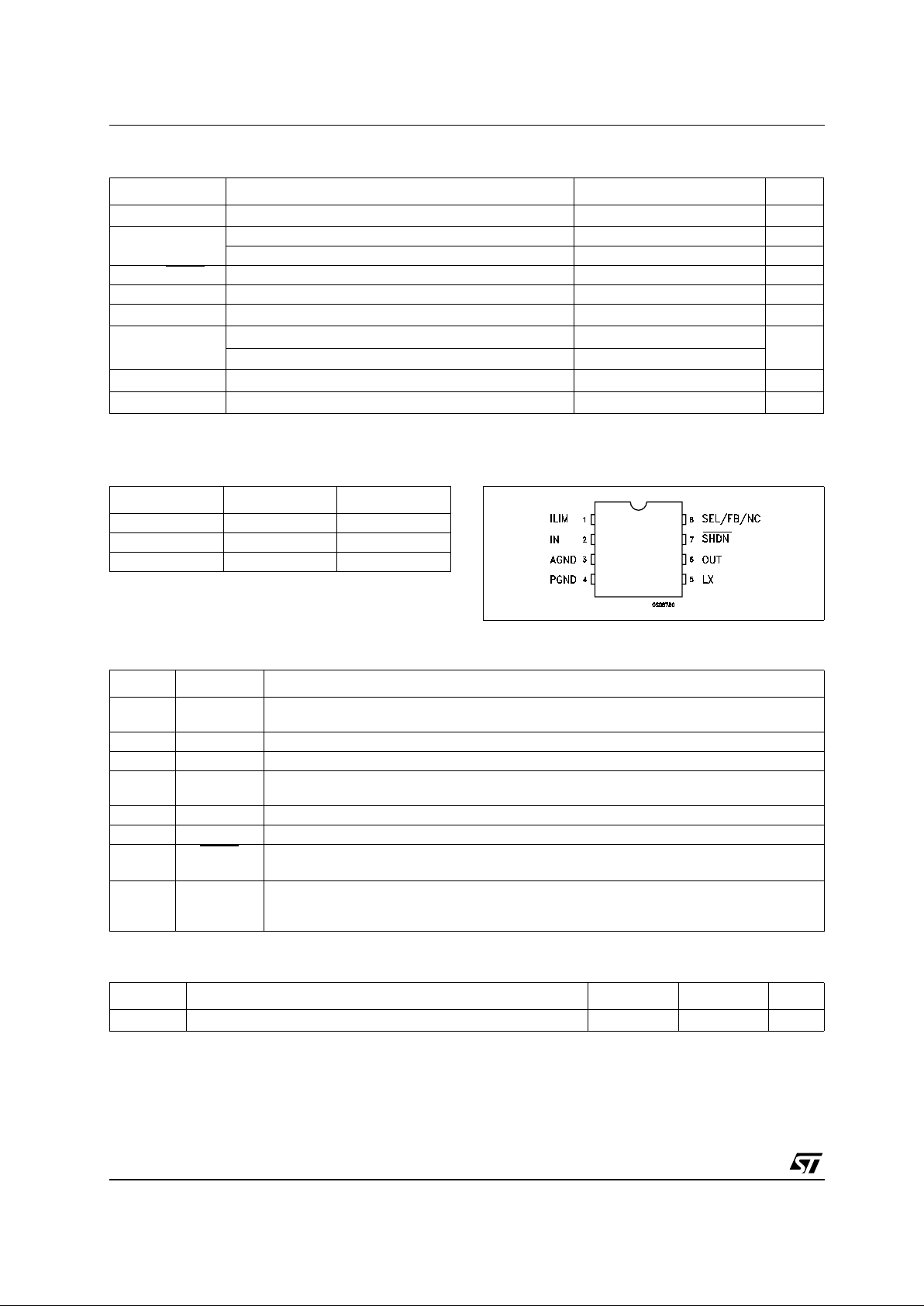
ILIM LX
IN
OUT
PGND
SEL
AGND
1
2
3
4
5
6
7
8
SHDN
1.25V
VREF
SHUTDOWN
CONTROL
DELAY
TIMER
DELAY
TIMER
t
OFF
tON
SWITCH
DRIVER
ACTIVE RECTIFIER
RECTIFIER
CONTROL
1:N
SCHEMATIC DIAGRAM
SO-8DIP-8
ST777/778/779
2/11
ABSOLUTE MAXIMUM RATINGS
Absolute Maximum Ratings are those values beyond which damage to the device may occur. Functional operation under these condition is
not implied.
ORDERING CODES CONNECTION DIAGRAM
PIN CO NNE CTIONS
THERMAL DATA
Symbol Parameter Value Unit
V
CC
DC Input Voltage to GND
-0.3 to +7 V
LX
Switch off Pin Voltage -0.3 to +7 V
Switch on Pin Voltage 30 sec short to IN or OUT
OUT, SHDN
Output, Shutdown Voltage -0.3 to +7 V
AGND to PGND Analog and Power Ground -0.3 to +0.3 V
FB FB Pin Voltage
-0.3 to (OUT+0.3) V
P
TOT
Continuous Power Dissipation (at TA= 85°C) DIP-8
550
mW
Continuous Power Dissipation (at T
A
= 85°C) SO-8
344
T
STG
Storage Temperature Range
-40 to 150 °C
T
OP
Operating Ambient Temperature Range
0to85 °C
TYPE DIP-8 SO-8
ST777 ST777ACN ST777ACD
ST778 ST778ACN ST778ACD
ST779 ST779ACN ST779ACD
Pin No. SYMBOL NAME AND FUNCTION
1 ILIM Sets switch current limit input. Connect to IN for 1A current limit. A resistor from ILIM to IN
sets lower peak inductor currents.
2 IN Input from battery
3 AGND Analog ground. Not internally connected to PGND.
4 PGND Power ground. Must be low impedance; solder directly to ground plane or star ground.
Connect to AGND, close to the device.
5 LX Collector of 1A NPN power switch and emitter of Sinchronous Rectifier PNP.
6 OUT Voltage Output. Connect filter capacitor close to pin.
7SHDN
Shutdown input disables power supply when low. Also disconnets load from input. Threshold
is set at V
IN
/2.
8 SEL/N.C./FB - Selection pin for 3/3.3V version (778);
- Not internally connected for 5V version (777);
- Feedback pin for adjustable version (779).
Symbol Parameter DIP-8 SO-8 Unit
R
thj-amb
Thermal Resistance Junction-ambient
100 160 °C/W
ST777/778/779
3/11
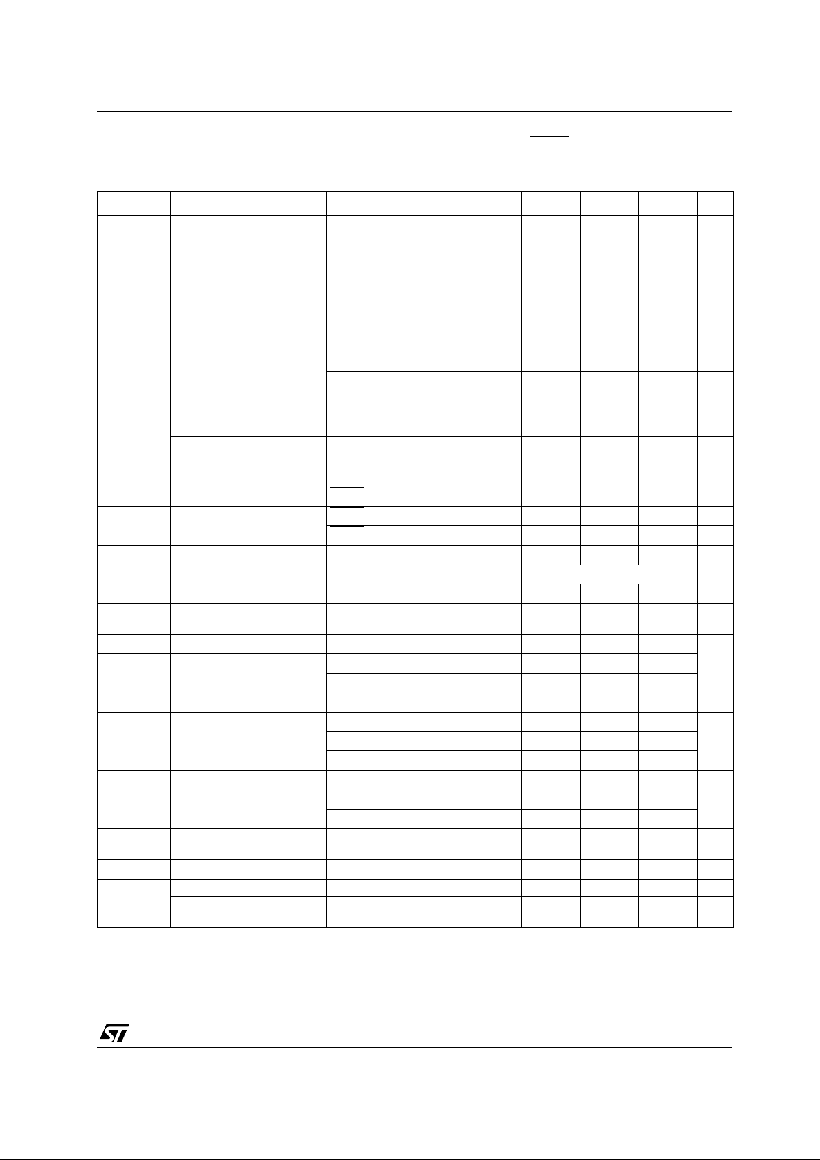
ELECTRICAL CHARACTERISTICS (VIN=2.5V, CI= 22µF, CO=100µF, SHDN and ILIM connected to IN,
AGND connected to P GND, T
A
=0 to 85°C, unless otherwise specified. Typical values are referred at
T
A
=25°C)
Note 1:Output in regulation, V
OUT=VOUT
(nominal) ± 4%.
Note 2:At hight V
IN
to V
OUT
differentials, the maximum load current is limited by the maximum allowable power dissipation in the package.
Note 3:Start-up guaranteed under these load conditions.
Note 4:Minimum value is production tested. Maximum value is guaranteed by design and is not production tested.
Note 5:In the ST779 supply current depends on the resistor divider used to set the output voltage.
Note 6:V
OUT
is set to a target value of +5V by 0.1% external feedback resistors. V
OUT
is measured to be 5V±2.5% to guarantee the error
comparatortrip point.
Symbol
Parameter
Test Conditions Min. Typ. Max. Unit
V
START
Start up Voltage I
LOAD
< 10mA, TA= 25°C (Note 1) 1 V
V
IN(MAX)
Maximum Input Voltage (Note 1,2) 6 V
V
O
Output Voltage ST777 779
(set to 5V), (Note 3)
I
LOAD
≤ 30mA, VIN = 1.1V to 5V or
I
LOAD
≤ 80mA, VIN = 1.8V to 5V or
I
LOAD
≤ 130mA, VIN = 2.4V to 5V
4.8 5.0 5.2 V
Output Voltage ST778
(Note 3)
SEL=0V
I
LOAD
≤ 50mA,VIN =1.1V to 3.3V or
I
LOAD
≤ 210mA,VIN =1.8V to 3.3V or
I
LOAD
≤ 300mA,VIN =2.4V to 3.3V
3.17 3.30 3.43 V
SEL=OPEN
I
LOAD
≤ 30mA, VIN =1.1V to 3V or
I
LOAD
≤ 210mA, VIN =1.8V to 3V or
I
LOAD
≤ 300mA, VIN =2.4V to 3V
2.88 3.00 3.12 V
Output Voltage Range
ST779
(Note 4)
2.7 6.5 V
I
IN
No Load Supply Current I
LOAD
= 0 mA, (Switch ON) (Note 5) 270 µA
I
SHDN
Shutdown Supply Current SHDN=0V, (Switch OFF) 20 35 µA
I
IN SHDN
Shutdown Input Current SHDN = 0 to V
IN
15 100 nA
SHDN
=VINto 5V 12 40 µA
υ Efficiency I
LOAD
=100mA 82 %
V
IH
Shutdown Input Threshold VIN=1V to 6V VIN/2 + 0.25 V
I
LIM
Current Limit 1.0 A
I
LIM TEMPCO
Current Limit Temperature
Coefficient
-0.3 %/°C
t
OFFMIN
Minimum Switch Off Time 1.2 µs
t
ONMAX
Maximum Switch ON Time VIN=2.5V 4.5
V
IN
=1.8V 6.5
V
IN
=1V 15
V
CESAT NPN
Switch saturation Voltage ISW=400mA 0.25 V
I
SW
=600mA 0.33
I
SW
=1000mA 0.5
V
CESAT NPN
Rectifier Forward Drop ISW=400mA 0.18 V
I
SW
=600mA 0.22
I
SW
=1000mA 0.4
V
FB
Error Comparator Trip Point ST779, over operating input
voltage (Note 6)
1.23±2% V
I
FB
FB Pin Bias Current ST779, VFB=1.3V 50 nA
I
LX
Switch Off Leakage Current 0.1 µA
Rectifier Off Leakage
Current
0.1 µA
ST777/778/779
4/11
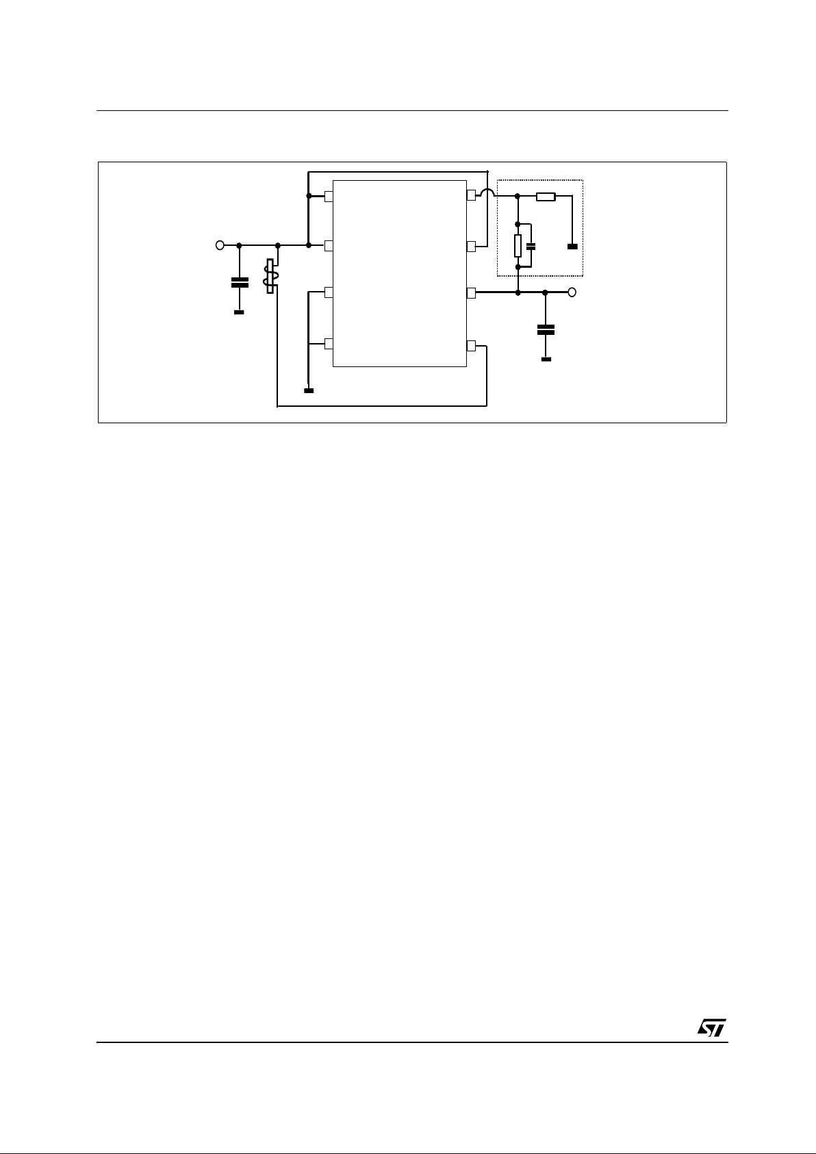
TYPICAL AP PLICATION CIRCUIT
APPLICATIONS INFORMATION
R1 and R2 must be placed only in ST779
applications to set the output voltage according to
the following equation:
V
OUT
= (1.23) [ (R1+R2)/R2]
and to simplify the resistor selection:
R1 = R2 [(V
OUT
/1.23)-1]
It is possible to use a wide range of values for R2
(10KΩ to 50KΩ) with no significant loss of
accuracy thanks to the very low FB input cu rrent.
To have 1% error, the current through R2 must be
at least 100 t im es FB ’s bias current.
When larg e values are used for the feedback
resistors (R1>50KΩ), stray output impedance at
FB can incidentally add "lag" to the feedback
response, destabilizing the regulator and creating
a larger ripple at the ou tput. Lead lengths and
circuit board traces at the FB node should be kept
short. Compensate the loop by adding a "lead"
compensation capacitor (C3, 100pF to 1nF) in
parallel with R 1.
The typica l value of t he L1 inductor is 22µH,
enough for most applications. However, are also
suitable values ranging from 10µF to 47µF with a
saturation rating equal to or greater than the peak
switch -current limit.
Efficiency will be reduced if the inductor works
near its saturation limit, while will be maximized
using an i nduc t or with a low DC resistance,
preferably under 0.2Ω.
Connecting ILIM to V
IN
the maximum LX current
limit (1A) is set. If this maximum value is not
required is possible to reduce it connecting a
resistor between ILIM and V
IN
(SeeFigure16to
choose the right value). The current limit value is
misured when the switch current through the
inductor begins to flatten and does ’nt coincide with
the max short circuit current.
Even if the device is designed to tolerate a short
circuit wi thou t any dam age, it is strictly
recommended to avoid a continuos and durabl e
short circuit of the output to GND.
To achieve the best performances f rom switching
power supply topology, particular care to layout
drawing is needed, in order to minimize EMI and
obtain low noise. Moreover, jitter f ree operation
ensures the full device functionality. Wire lengths
must be minimized, filter and by-pass capacitors
must be low ESR type, placed as close as
possible to the integrated circuit. Solder AGND
and PGND pins directly to a ground plane.
ST777
ST778
ST779
ILIM
L1
22µH
SEL / N.C. / FB
R1
V+
LX
Vout
SHDN
____
AGND
C1
22µF
C2
100µF
C3
Vin
1÷6V
1
3
8
7
2
5
6
4
Vo
PGND
R2