

SGS Thomson Microelectronics ST75C540, ST75C530 Datasheet
ST75C530
ST75C540
SUPERINTEGRATED DEVICESWITHDSP,AFE& MEMORIES
FOR TELEPHON Y, MODEM, FA XOVERINTERNET& POTSLINES
SUMMARIZED FEATURES
(fordetailed features,see page 4)
.
SINGLECHIP FAXUp to 14.4Kbps(V.17)
.
FULL DUPLEX DATA MODEM UP TO
14.4Kbps(V.32Bis)
.
DIGITALANSWERING MACHINE :
- 4.8Kbps VOCODER
- VAR IABLEPLAYBACKSPEED(+50%to -50%)
-ADPCM 32, 34, 16KbpsVOCODER
.
FULL-DUPLEX DIGITAL SPEAKERPHONE
WITHECHO CANCELLATION
.
PROGRAMMABLERING DETECTION
.
16 PROGRAMMABLE TONE DETECTORS
FORCLID AND SCWID
.
DTMFDETECTION
.
VERSATILEHOSTINTERFACES
.
16 GENERALPURPOSEI/O PORTS
.
2 RELAYDRIVE OUTPUTS
.
SINGLE5V POWER SUPPLY
.
TYPICALACTIVEPOWERCONSUMPTION:
650mW(ST75C530),750 mW(ST75C540)
.
LOWPOWER MODE < 30mW
.
80-PINTQFPPACKAGE (14mmx 14mm)
DESCRIPTION
ST75C530 and ST75C540 are two super-integrated devices including DSP, Modem and Audio
Analog Front Ends and memories for Telephony,
Modemand FAXapplications.
These devices can be used for classical applicationsover POTSlines or over Internet.
The super integration technology allows a significant cost reduction on bill of materials for equipment like High-End phones, INTERNET phones,
phone-Fax,INTERNET FAX, ...
The devices are used with a host processor
througha Dual Port RAM allowing the use of any
kind of microcontroller(RISC, CISC,General Purpose 8-bitµC, ...).
The embedded software includes :
- handsetwith listeninggroup capability,
- fullduplex handsfree,
- voicecoder/decoderat 4.8Kbpsforstaticanswering machine applications and ADPCM 16Kbps,
24Kbps and 32Kbps for high quality message
recording,
- Tone and DTMF generators,
- Tone and DTMF detectors,
- FAX up to 14.4Kbps,
- Data-Modemup to 14.4Kbps(ST75C540 only).
The DSPsofware is extensively user configurable
allowing specific functions to be supported like
Caller Identifier (CLID) and Second Call Waiting
Identifier(SCWID).
The DSP software includes a transparent mode
allowing the host controller to access directly the
modem Analog Front End and the Audio AFE
through the dual Port RAM.This is very useful for
hostprocessingmodem solutions (orsoft modem)
wherethe modulationandthedemodulation(V.34,
V.90)are done by the applicationmain processor.
In transparentmode, the embedded DSP can be
used simultaneouslywith the same samples.
Thetransparentmode for audioAFEis providedto
play audio filesor to recordvoice and/oraudio.
TQFP80 (14 x14 x 1.4mm)
(Full Thin Plastic Quad Flat Pack)
ORDER CODE : ST75C530FP-A
ST75C540FP-A
February 1999
1/84

ST75C530- ST75C540
CONTENTS Page
I DETAILED FEATURES ................................................. 4
II PIN DESCRIPTION .................................................... 5
II.1 PIN CONNECTIONS. . .. ................................................ 5
II.2 HOST INTERFACE. .................................................... 6
II.3 ANALOGINTERFACE . ................................................. 6
II.4 GENERALPURPOSEIO ANDRELAY . . .. ................................. 6
II.5 MISCELLANEOUS. .................................................... 7
II.6 POWER SUPPLY . . . . . . . . . . . . .. . . . .. . . . . . . . . ........................... 7
III BLOCK DIAGRAMS.................................................... 8
III.1 ANALOGINTERFACE . ................................................. 8
III.2 INTERNALBLOCK DIAGRAM . ........................................... 8
IV ELECTRICAL SPECIFICATIONS ......................................... 9
IV.1 MAXIMUMRATINGS................................................... 9
IV.2 RECOMMENDED OPERATINGCONDITIONS. . . . . . . . . ...................... 9
IV.3 DIGITALINTERFACE. . . . . . . . . . . . .. . . . .. . . . ............................. 10
IV.4 MODEMANALOGINTERFACE. . . . ....................................... 11
IV.5 AUDIOANALOG INTERFACE . ........................................... 11
IV.6 AC CHARACTERISTICS . . .. . . . .. . . . . . . . . . . . . . . ......................... 12
V FUNCTIONAL DESCRIPTION............................................ 13
V.1 SYSTEMARCHITECTURE . . . . .......................................... 13
V.2 MODES OF OPERATION. . .. . . . .. . . . . . . . . . . . . . . ......................... 13
V.3 OPERATIONS. . . . . . . . . . . . . . . . . .. . . . . . ................................. 13
V.3.1 ModemTransmitterDescription . . .. ....................................... 13
V.3.2 ModemReceiver Description . . .. . . . .. . . . .. . . .. . . . .. ...................... 13
V.3.3 Tone GeneratorDescription . . . . .......................................... 13
V.3.4 Tone Detector Description . .............................................. 13
V.3.5 V.21 Channel2 FlagDetectorDescription . .................................. 13
V.3.6 HDLC Description . . . . . . . . . . . . .. . . . .. . . . . . . . . ........................... 13
V.3.7 UARTDescription . . . . . . . . . . . . .. . . . .. . . . . . . . . ........................... 13
V.3.8 DTMF Detector Description. .............................................. 13
V.3.9 Ring Detector . . . . . . . . . . . . . . . . . . . . . . . . ................................. 13
V.3.10 VOCODERDescription. ................................................. 14
V.3.11 VoiceActivity Detector(VAD). . . . . . . . . . . . .. . . . . . . . .. ...................... 14
V.3.12 Telephony Functions. . . . ................................................ 15
V.3.13 Low PowerMode . . . . . . . . . . . . . . . . . . . . . . . . . . . ........................... 18
V.3.14 Reset. . . . . . . . .. . . . . .............................................. .... 18
V.4 MODEMINTERFACE. . .. . . . . . . . . . . . . . . . . . . ............................. 18
V.4.1 AnalogInterface . . . . ................................................... 18
V.4.2 GeneralI/O and Relay Interface. . . . ....................................... 18
V.4.3 Crystal. ........................................................... ... 19
V.4.4 TypicalApplicationSchematic. . . . . . . . . . . . . . . . . . . . . . . ...................... 19
V.4.5 Host Interface . . . . . . . . . . . . . . . . . . . . . . . . ................................. 19
VI USER INTERFACE..................................................... 21
VI.1 DUAL PORT RAMDESCRIPTION. ........................................ 21
VI.2 COMMANDSET. . . . ................................................... 25
VI.3 COMMANDSET SHORT FORM . . . . . . . . . . . . .............................. 26
VI.4 STATUS- REPORTS. . . . . . . . . . . . . . . . . . . . . . ............................. 27
VI.5 DATA EXCHANGES. . .. ................................................ 27
2/84

ST75C530- ST75C540
VII COMMAND SET DESCRIPTION.......................................... 28
VIII STATUS DESCRIPTION ................................................ 43
VIII.1 COMMANDACKNOWLEDGEAND REPORT. . . . . . .......................... 43
VIII.2 MODEMSTATUS. . .. . . . . . . . . . . . . . . . . . . . . . .. ........................... 44
IX TONE DETECTORS.................................................... 53
IX.1 OVERVIEW. .......................................................... 53
IX.2 DESCRIPTION. ....................................................... 53
IX.3 EXAMPLE. . . . . . . .. . . . .. . . . . . . . . . . .................................... 59
X PARALLELDATA EXCHANGE........................................... 60
X.1 OVERVIEW. .......................................................... 60
X.2 TRANSMITBUFFER . . .. . . . . . . . . . . . . . . . . . . ............................. 60
X.3 RECEIVEBUFFER. .................................................... 61
X.4 INTERRUPTION. . . . ................................................... 61
X.5 DATA FORMAT . . . . ................................................... 61
X.6 FORMCOMMAND . .................................................... 63
XI TRANSMITTING DATAIN PARALLELMODE ............................... 64
XI.1 DESCRIPTION. ....................................................... 64
XI.2 MODEMFLOW CHART . . . . ............................................. 65
XI.3 HOST FLOW CHART. . . . . . . . . . . . . . . . . . . . . . ............................. 65
XI.4 ERROR DETECTION. . .. . . . . . . . . . . . . . . . . . . ............................. 66
XI.5 SYNCHRONOUS MODE . . . . . . . . . . . . . . . . . .. . . . . ......................... 66
XI.6 HDLC MODE. . . . ...................................................... 67
XI.7 UARTMODE DESCRIPTION. . . . . . . .. . . . .. . . .. . . . .. ...................... 69
XII RECEIVINGIN PARALLEL MODE ........................................ 70
XII.1 DESCRIPTION. ....................................................... 70
XII.2 MODEMFLOW CHART . . . . ............................................. 70
XII.3 HOST FLOW CHART. . . . . . . . . . . . . . . . . . . . . . ............................. 70
XII.4 ERROR DETECTION. . .. . . . . . . . . . . . . . . . . . . ............................. 71
XII.5 SYNCHRONOUS MODE . . . . . . . . . . . . . . . . . .. . . . . ......................... 72
XII.6 HDLC MODE. . . . ...................................................... 72
XII.7 UARTMODE. . . . ...................................................... 74
XIII VOCODERDATA EXCHANGE ........................................... 74
XIII.1 OVERVIEW. .......................................................... 74
XIII.2 VOCODERBUFFER. . .. ................................................ 74
XIII.3 TRANSMIT(DECODER) . . . . . . . . . . . . .. . . . .. . . .. ......................... 74
XIII.4 RECEIVE(CODER) . . .. ................................................ 75
XIV TRANSPARENTMODE DATA EXCHANGE................................. 75
XV DEFAULT CALL PROGRESS TONE DETECTORS........................... 76
XVI DEFAULT ANSWER TONEDETECTORS .................................. 76
XVII ELECTRICAL SCHEMATICS............................................. 77
XVIII PCB DESIGN GUIDELINES.............................................. 78
XIX APPENDIX A : MODESOF OPERATION . .................................. 78
XX PACKAGE MECHANICAL DATA ......................................... 83
3/84

ST75C530- ST75C540
I - DETAILED FEATURES
SingleChip Fax
- ITU-T V.17, V.29,V.27ter,V.21with Fax support
- V.17, V.29 (T104), V.27ter short trains,
V.33 half-duplex
- V.21 flag detection and 4 tone detection during
high speedreception modes
- V.21 flag detection, DTMF detection and 4
tone detection duringV.21channel2 reception
modes
- Programmable call progress and call waiting
detection
- Parallel data handling
- HDLC and UART framingsupport
- 1700Hz and 1800Hz carrier
- Full implementation of the V.17, V.33, V.29 and
V.27handshakes
- 0 to -15dBmprogrammabletransmitpower
- 0 to-47dBmreceiverdynamicrange(ST75C530)
0 to-45dBmreceiverdynamicrange(ST75C540)
Handset Mode
- Rx and Tx AGC versus line current for line
losses compensation comply with most of
country regulations
- Dynamic limiter in transmit path to prevent
distortion
- Two wayconversationrecording
Hands-freeMode
- Fullduplex speakerphoneusing LMSadaptative
filtering including line echo cancellation and
acoustic echo cancellation
- Rx and Tx AGC versus line current for line
losses compensation comply with most of
country regulations
- Dynamic limiter in transmit path to prevent
distortion
- Loudspeakervolume control
- Two wayconversationrecording
Full Duplex Data Modem
- ITU-T V.32bis, V.32 (14400,12000, 9600, 7200,
4800bps) (*)
- Maximum round trip delay : 1.2s (satellite hops)
(*)
- Up to 10Hzof phaseroll on far end echo (*)
- ITU-T V.22bis,V.22(2400, 1200bps)(*)
- V.32bis/V.32/V.22bis/V.22automode(*)
- ITU- V.23,V.21,bell103 full-duplex,
Bell202 demodulator
- -10 to -25dBmprogrammabletransmit power
- -10to-38dBmreceiverdynamicrange(*)
- HDLC and UART framingsupport
- Train based on qualityline sampling(*)
(*)ST75C540 only
DigitalAnsweringMachine
- Low bit ratespeech coder(4800bps)
- Variableplaybackspeed (+50%to -50%)
- ARAM compatibility (errorcorrection)
- ADPCM 32, 24, 16Kbps
- Line echo cancellation
- Voice activity detector
- ConcurrentDTMF and tonedetection
ExtendedModes of Operations
- Programmablering detection
- 16 programmabletone detectors
- Toneand DTMF generators
- Caller ID reception
- Transparentmode allowingdirect transferof Modem AFE and audio AFE samples to and from
host processor for soft Modem applicationsand
sound files playing
- DTMFdetection
- Wide dynamicrange (>48dB)
VersatileInterfaces
- Parallel 128 x 8-bit dual port RAM
- Generalpurpose16 I/Oports
- 2 relay drive outputs
- Fulldiagnostic capability
- Dual 8-bit DACfor constellationdisplay
Single 5V PowerSupply
- Typicalactive powerconsumption:
650mW (ST75C530),725mW (ST75C540)
- Low power mode < 30mW
4/84
II - PINDESCRIPTION
II.1 - Pin Connections
ST75C530- ST75C540
SPK1N
SPK1P
AGNDTA
V
REFN
V
REFP
V
AGNDRA
MIC1
MIC2
MIC3
RxA
AV
DDM
AGNDM
TxA2
TxA1
EYEX
EYEY
DGND6
DV
DD6
DGND1
DDA
SPK2P
SPK2N
SPK3P
SPK3N
RESET
TEST0
AV
EXTALL
7677787980
1
2
3
4
5
CM
6
7
8
9
10
11
12
13
14
15
16
17
18
19
20
DD5
XTALL
DV
DGND5
XPLL
CLKOUT
GIO17
GIO16
GIO15
6566676869707172737475
GIO14
GIO13
GIO12
GIO11
61626364
60
59
58
57
56
55
54
53
52
51
50
49
48
47
46
45
44
43
42
41
GIO10
DV
DD4
DGND4
GIO07
GIO06
GIO05
GIO04
GIO03
GIO02
DV
DD3
DGND3
GIO01
GIO00
RING
RELAY1
RELAY0
RGND
INT/MOT
SINTR
SCS
DD1
DV
SD0
SD1
SD2
26 27 28 29 30 31 32 33 34 35 3621 22 23 24 25
SD3
SD4
SD5
SD6
SD7
DD2
DV
DGND2
SR/W
SDS
SA0
37 38 39 40
SA1
SA2
SA3
SA4
SA5
SA6
75C53001.EPS
5/84
ST75C530- ST75C540
II - PIN DESCRIPTION(continued)
II.2 -Host Interface
Theexchangeswiththecontrolprocessor proceedthrougha 128 x8 DUALport RAMsharedbetween the
ST75C530/540and the Host. The signals associatedwith thisinterfaceare :
Pin Name Type Description
SD0..SD7 I/O System Data Bus. 8-bit data bus used for asynchronous exchanges between the
SA0..SA6 I System Address Bus. 7-bit address bus for dual port RAM, IO and interruptregisters.
SDS (SRD) I System DataStrobe. In Motorola mode SDS initiates the exchange, active low. InIntel mode
SR/W (SWR) I System Read/Write.In Motorola mode SR/W defines the type ofexchange read/write. In Intel
SCS I System Chip Select. Active low.
SINTR OD System InterruptRequest. Opendrain. Activelow.Thissignal isasserted by theST75C530/540
RESET I Reset. Active low.
INT/MOT I Select Intelor MotorolaInterface
II.3 -AnalogInterface
Pin Name Type Description
TxA1 O Transmit Analog Output 1
TxA2 O Transmit Analog Output 2
RxA I Receive Analog Input
SPK1P O Speaker Output 1, (differential positive), must be connected through Amplifier to the
SPK1N O Speaker Output 1, (differentialnegative)
SPK2P O Speaker Output 2, (differentialpositive), must be connected through Amplifier to the Handset
SPK2N O Speaker Output 2, (differentialnegative)
SPK3P O Speaker Output 3, (differential positive)
SPK3N O Speaker Output 3, (differentialnegative)
MIC1 I Microphone Input 1
MIC2 I Microphone Input 2
MIC3 I Microphone Input 3
V
CM
V
REFN
V
REFP
ST75C530/540 and the Host through the dual port RAM. High impedance when exchanges
are not active.
SRD initiates a read exchange,active low.
mode SWR initiates a write exchange, active low.
and negated by the host.
loudspeaker.
loudspeaker.
I/O AnalogCommon Voltage (nominal+2.5V).Thisinput must bedecoupled withrespect toAGND.
I Analog Negative Reference (nominal 1.25V). This input must be decoupled with respect to
I Analog Positive Reference (nominal 3.75V). This inputmust be decoupled with respect to VCM.
.
V
CM
II.4 -General Purpose IO and Relay
Pin Name Type Description
GIO[0,7] I/O General Purpose I/OPins, can be independently selected as input or output.
GIO[10,17] I/O General Purpose I/OPins, can be independently selected as input or output.
RELAY0,
RELAY1
RING I Ring detectsignal. Activelow.If the ST75C530/540 is inlow powermode,alow levelwill awake
RGND PWR Relay Digital Ground. To connect to GND.
6/84
OD Relay Outputs, Open Drain, Active Low. Can sink -10mAto RGND.
the chip. Thisinput is a Schmidt’s trigger.
ST75C530- ST75C540
II - PIN DESCRIPTION(continued)
II.5 -Miscellaneous
Pin Name Type Description
EYEX O Constellation X analog coordinate
EYEY O Constellation Y analog coordinate
XTAL O Internal Oscillator Output. Left open if not used.
EXTAL I Internal OscillatorInput, orExternal Clock Input.
XPLL I Reserved for future use, must beconnected to digital ground.
CLKOUT O Output Clock, EXTAL/2(not availablein low power mode).
TEST0 I Test pin for normal operation, must be connected todigital ground.
Note : Thenominal frequency of the crystal oscillator is 44.2368MHz witha precision betterthan ± 100ppm.
II.6 -Power Supply
Symbol Nber Parameter
DV
DD
DGND 6 Digital Ground.
AV
DD
AGND 3 Analog Ground.
6 Digital +5V.
2 Analog +5V.
7/84
ST75C530- ST75C540
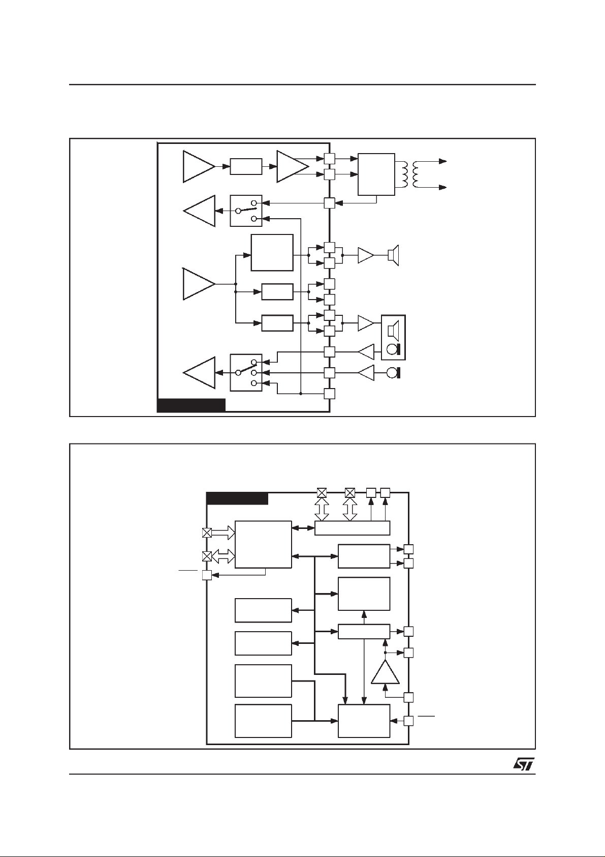
III - BLOCK DIAGRAMS
III.1- Analog Interface
TXA1
MUTEDAC
15
14
TXA2
HYBRID
Line
ADC
DAC
ADC
ST75C530/540
III.2 - InternalBlock Diagram
[0..-30]dB
Step 3dB
ST75C530/540
MUTE
MUTE
MUTE
11
76
77
78
79
10
Pins 48-49
Pins 52 to 57
RXA
1
2
SPK1
SPK3
SPK2
9
MIC2
8
MIC1
MIC3
GIO0[0..7]
Pins 60 to 67
GIO1[10..17]
45 46
RELAY0
RELAY1
75C53002.EPS
8/84
Pins 34 to 40
SA[0..6]
Pins 22 to 29
SD[0..7]
SINTR
GIO ANDRELAY
DUAL
PORT RAM
42
Data Bus
RAM
6144 WORDS
ROM
16368 WORDS
PROM
26624
INSTRUCTIONS
AUTOTEST
AUTOTEST
1024
1024
INSTRUCTIONS
INSTRUCTIONS
Bus
Instruction
EYE DAC
ANALOG
FRONT
END
TIME BASE
ST18932
DSP
(24Mips)
OSC
16
17
68
72
73
47
EYEX
EYEY
EYEY
CLKOUT
XTAL
EXTAL
RING
75C53003.EPS
ST75C530- ST75C540
IV- ELECTRICALSPECIFICATIONS
IV.1 - MaximumRatings (AGND= DGND= RGND= 0V,all voltageswith respectto 0V)
Symbol Parameter Value Unit
AV
DV
I
I
V
V
V
IDGPIO
T
oper
T
P
Warning : Operation beyond these limits may result in permanent damage to the device. Normal operation isnot guaranted atthese extremes.
IV.2 - RecommendedOperatingConditions
(AGND= DGND = RGND= 0V,all voltageswith respect to 0V)
Symbol Parameter Min. Typ. Max. Unit
V
I
P
P
V
I
CM
Note 1 : DCcurrent only. If dynamic loadexists, the VCMoutputmust be buffered or the performances of ADCs andDACs will be degraded.
Analog Power Supply -0.3, 6.0 V
DD
Digital Power Supply -0.3, 6.0 V
DD
I
Input Current per Pin (except supply pins and RELAY0and RELAY1) -10, +10 mA
I
Output Current per Pin (except supply pins and RELAY0and RELAY1) -20, +20 mA
O
Output Current per Pin RELAY0or RELAY1 (respect toRGND) -40, 0 mA
O2
Analog Input Voltage -0.3, AVDD+ 0.3 V
IA
Digital Input Voltage -0.3, DVDD+ 0.3 V
ID
Digital Input Voltage at GPIO 5.25 V
Operating Temperature 0, +70 °C
Storage Temperature - 40, +125 °C
stg
Maximum Power Dissipation 1500 mW
tot
Supply Voltage 4.75 5 5.25 V
DD
Supply Current ST75C530
DD
Low Power 30 mW
DLP
Power ST75C530
D
Common Mode Voltage Output (refer to AVDD/2) -5 +5 %
CM
ST75C540
ST75C540
130
145
650
725
Common Mode Current (see Note 1) 100 µA
150
165mAmA
790
866mWmW
9/84
ST75C530- ST75C540
IV- ELECTRICALSPECIFICATIONS (continued)
IV.3 - Digital Interface
=DVDD= 5V,AGND= DGND= RGND = 0V) exceptXTAL, EXTAL,RING.
(AV
DD
Symbol Parameter Min. Typ. Max. Unit
V
V
V
V
I
LEAK
I
I
OH
I
I
I
OLRELAY
CRYSTAL OSCILLATOR
High Level Input Voltage 2.2 V
IH
Low LevelInput Voltage -0.3 0.8 V
IL
High Level Output Voltage (I
OH
Low LevelOutput Voltage (I
OL
load
load
= -2mA, I
= 2mA, I
= -4mA for SD[7..0]) 2.4 V
load
= 4mA forSD[7..0]) 0.4 V
load
Input Leakage Current -10 10 µA
Low LevelOutput Current (except RELAY0 and RELAY1, andSINTR)
OL
(0 < V
OL<VOLMax.
)
-2 mA
High Level Output Current (except RELAY0 and RELAY1, and SINTR)
(0 < V
OL<VOLMax.
GIO ThreeState Input Leakage Current (GND < VO<VDD) -50 0 50
OZ
SD Three State InputLeakage Current (GND < VO<VDD) -50 0 50 µA
OZ
)
Low LevelOutput Current RELAY0or RELAY1(VOL= 0.8V) -10 0 mA
2mA
A
µ
V
V
I
High Level Input Voltage 3.5 V
IH
Low LevelInput Voltage 1.5 V
IL
High Level Input Current -20 µA
H
I
Low LevelInput Current 20
L
RING (this input have hysteresis)
V
V
I
High Level Input Voltage 2.4 2.8 V
IH
Low LevelInput Voltage 1 1.2 V
IL
High Level Input Current -20
H
I
Low LevelInput Current 20 µA
L
A
µ
A
µ
10/84
ST75C530- ST75C540
IV- ELECTRICALSPECIFICATIONS (continued)
IV.4 - Modem Analog Interface
=DVDD=5V,T
AV
DD
Measurementbandwidthis flat from 100Hz to 4800Hz ;Load impedance10kΩ, 20pF
Fordifferentialoutput (TxA1/TxA2) : 0dBr = 1.77V
Forsingle input(RxA) : 0dBr= 886mV
Symbol Pin Name Parameter Min. Typ. Max. Unit
Rxrin RxA Input Impedance 100 kΩ
Rxmac Maximum AC Input Voltage = 0dBr 2.5 V
Rxdc DC Reference Voltage 2.5 V
Rxsndr Signalto (Noise + Distortion), at -6dBr 75 dB
Rxin Idle Noise -81 dBr
Rxov DC Offset Voltage (Input = V
TxAdrl TxA1/TxA2 Minimum Differential Load 10 kΩ
TxAcl Maximum Differential Load 20 pF
TxArout Output Impedance 100
TxAmac Maximum AC Differential Output = 0dBr 5 V
TxAdc DC Reference Voltage 2.5 V
TxAov DC Offset Voltage -200 200 mV
TxAsndr Signal to (Noise + Distortion), at -6dBr 79 dB
TxAin Idle Noise -85 dBr
amb
=25oC
1kHzsinwave (equivalentto 5VPP).
RMS
1kHzsinwave (equivalent to 2.5VPP).
RMS
) -50 100 mV
CM
PP
Ω
PP
IV.5 - AudioAnalogInterface
AV
=DVDD=5V,T
DD
amb
=25oC
Measurementbandwidthis flat from 100Hz to 4800Hz ;Load impedance10kΩ, 20pF
Fordifferentialoutput (SPK1N/SPK1P,SPK2N/SPK2P,SPK3N/SPK3P): 0dBr = 1.77V
(equivalentto 5V
Forsingle input(MIC1, MIC2, MIC3) : 0dBr = 886mV
Symbol Pin Name Parameter Min. Typ. Max. Unit
RArin MIC1,
RAmac Maximum AC Input Voltage = 0dBr 2.5 V
RAdc DC Reference Voltage 2.5 V
RAdis Distortionat -6dBr 2 %
RAin Idle Noise -81 dBr
RAov DC Offset Voltage (Input = V
TAdrl SPK1N/SPK1P,
TArout Output Impedance 100
TAmac Maximum AC DifferentialOutput = 0dBr 5 V
TAdc DC Reference Voltage 2.5 V
TAov DC Offset Voltage -200 200 mV
TAdis Distortion at -6dBr 1 %
TAin Idle Noise -81 dBr
).
PP
MIC2,
MIC3
SPK2N/SPK2P,
SPK3N/SPK3P
1kHz sinwave (equivalent to 2.5VPP).
RMS
Input Impedance 100 kΩ
) -50 50 mV
CM
Minimum Differential Load 10 kΩ
1kHzsinwave
RMS
PP
Ω
PP
11/84
ST75C530- ST75C540
IV- ELECTRICALSPECIFICATIONS (continued)
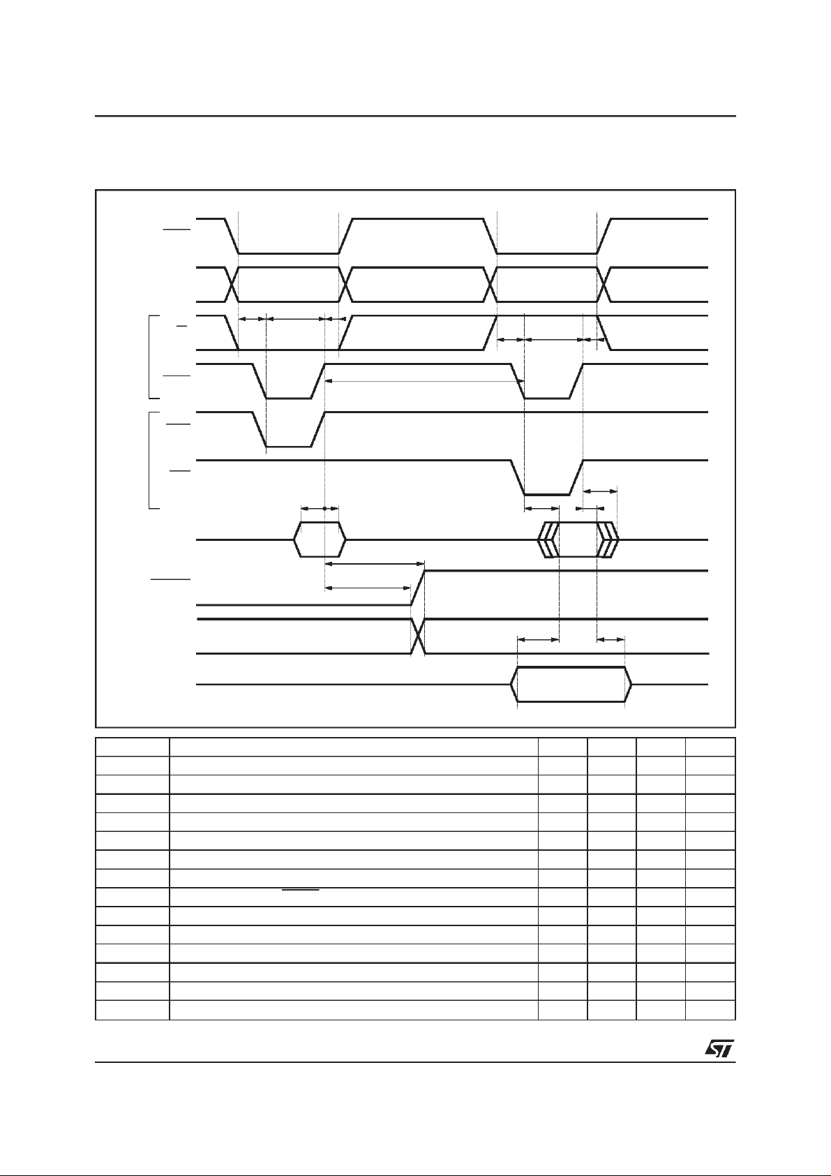
IV.6 - AC ElectricalCharacteristics
WRITE CYCLE READ CYCLE
SCS
SA[0..6]
SR/W
SDS
Motorola mode
WR
RD
Intel mode
SD[0..7]
SINTR
GIO(out),
RELAY
GIO(in)
132
67
8
9
5
142
11
10
13 14
12
OUTIN
75C53004.EPS
Number Description Min. Typ. Max. Unit
1 Address and Control Set-up Time 5 ns
2 Address and Control Hold Time 20 ns
3 Write Enable Low State 45 ns
4 Read Enable Low State 45 ns
5 Access Inhibition High State 70 ns
6 Data Set-up Time 10 ns
7 Data Hold Time 5 ns
8 GIO Output, Relay, SINTR Clear Delay 50 ns
9 GIO Output Hold Time 0 ns
10 Read Data Access Time 35 ns
11 Data Valid to Tristate Time 15 ns
12 Data Hold Time 5 ns
13 GIO Input Delay Time 40 ns
14 GIO Input Hold Time 0 ns
12/84

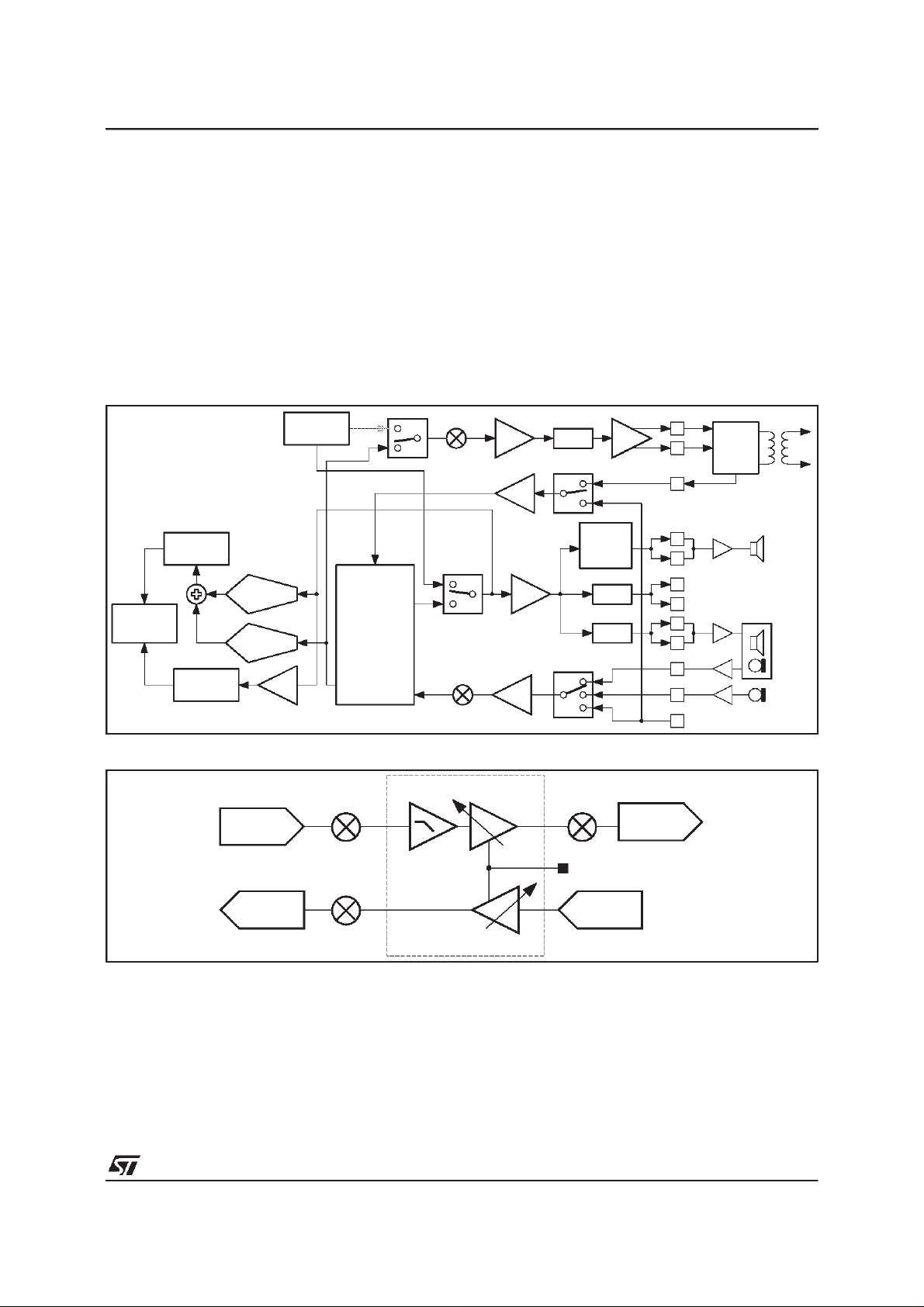
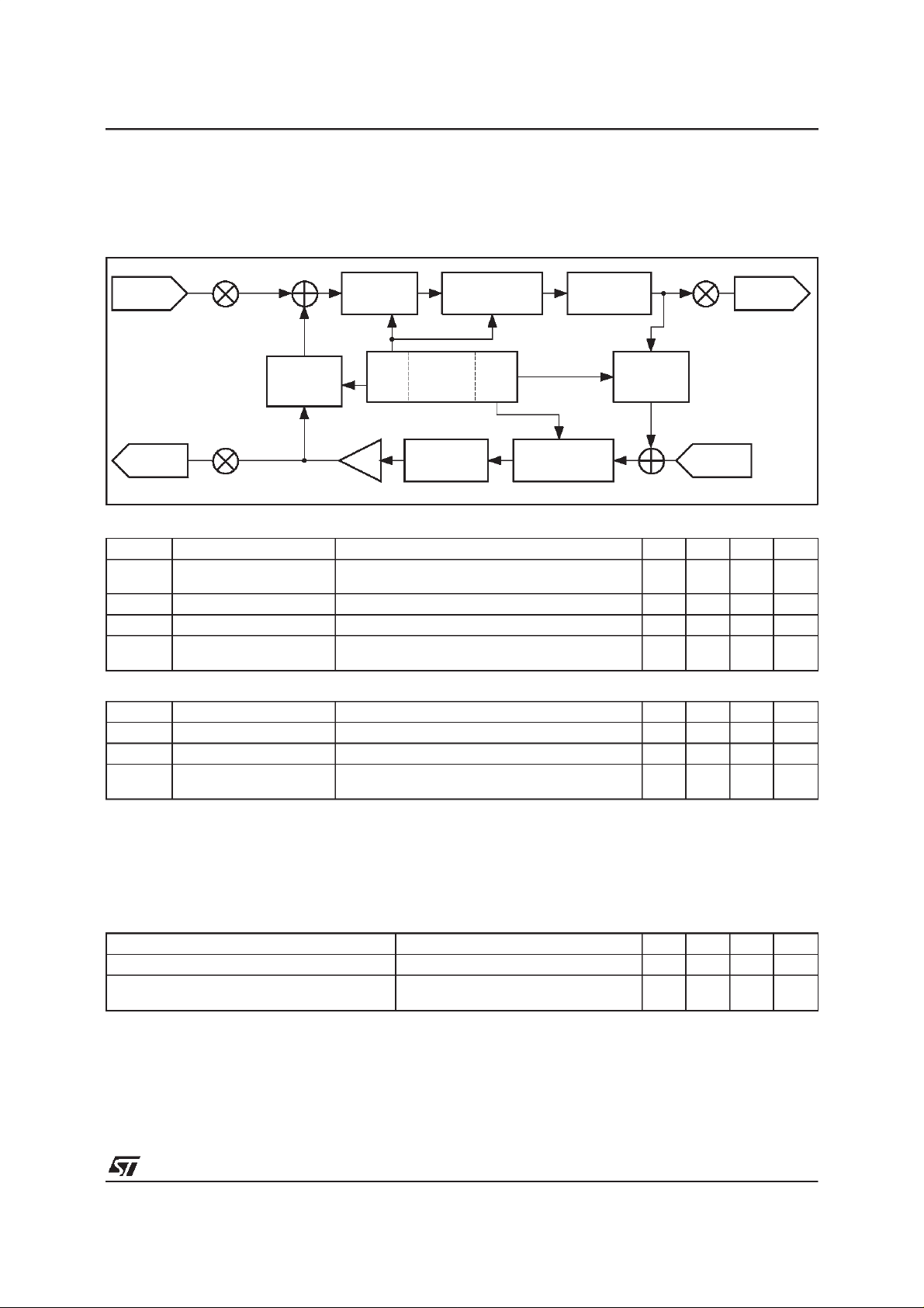
V - FUNCTIONALDESCRIPTION
V.1 - System Architecture
Thechipallowsthe designofa completeFAX,Data
Modem, Hands-Free Telephone and Answering
Machinesystem.A versatile dual port RAM allows
an easy interfacewith most micro-controllers.
V.2 - Modes of Operation
Referto AppendixA for BlockDiagrams.
V.3 - Operations
V.3.1 - Modem TransmitterDescription
The signal pulses are shapedin a dedicated filter
further combined with a compromise transmit
equalizersuited fortransmissionover stronglydistortedlines.3 differentcompromiseequalizersare
availableand can be selectedby software.
V.3.2 - Modem Receiver Description
Thereceiver section handlescomplex signals and
uses a fractionallyspacedcomplex equalizer. It is
able to copewith distant modem timing driftsup to
-4
asspecified in the ITU-Trecommendations.It
10
also compensatesfor frequency drift up to 10Hz
and for phase jitter at multiple and simultaneous
frequencies.
V.3.3 - Tone GeneratorDescription
Fourtonescanbesimultaneouslygeneratedby the
ST75C530/540. These tones are determined by
theirfrequenciesandbytheoutputamplitudelevel.
A set of specific commandsare also available for
DTMFgeneration.Anyof the4 tonegeneratorscan
be output independentlyeither on the Audio DAC
or the line DAC.
V.3.4 - Tone DetectorDescription
During TONE (respectively TONECID) Mode sixteen (respectively eight) tones can be simultaneouslydetected by the ST75C530/540.Each of the
tonesto be detectedis defined by the coefficients
ofa 4th orderprogrammableIIR. Detectionthresholdsare programmablefrom -51dBmupto -6dBm.
These primary detectors can detect tone up to
3.3kHz(sampling rate 7.2kHz in all modes). They
also have a programmable internalwiring feature
(seeChapter IX).
Inallmodes,exceptHandset(HANDSET)andFull
Duplex V.32bis/V.32/V.22bis/V.22 (Modem)
modes, 4 additional tone detectors (each of them
being a 4th order programmable IIR) are concurrently running. In Handset mode only 2 additional
tone detectorsare available. Detection thresholds
areprogrammablefrom-51dBmup to-6dBm.This
secondary programmable detector can detect
tones up to 1.8kHz by default set-up with a sam-
ST75C530- ST75C540
pling rate at 4.8kHz. But this 4 additional tone
detectorscan also detect tonesup to 3.3kHz with
a samplingrate at 9.6kHz. In order to avoid wrong
detectgion,relativedetectgionis also provided.
V.3.5- V.21Channel2 FlagDetectorDescription
InalltheReceiveFAXModes,includingV.21Channel 2 Mode, the ST75C530/540 processes a V.21
Flag“7E” detector,eitherin the idle state,the train
sequenceor the data mode. The detection timeis
3 consecutive flags to detect and 1 byte to loose
the detection.
V.3.6 - HDLC Description
In all FAXModes (MODEM), including V.21 Channel 2 Mode, and also Full Duplex
V.32bis/V.32/V.22bis/V.22 (Modem) modes, a
HDLC framing and deframing is supported by the
ST75C530/540. The number of transmitted flags
canbe programmed.
V.3.7 - UART Description
In Full Duplex V.32bis/V.32/V.22bis/V.22 Modem
ModesandTONECIDV.23receivemode,aparallel
UART is performed by the ST75C530/540. This
UARTmanagethe Break signaleitherat thetransmit and the receive bit stream. The Data format
supportedare7 and 8 bit of Data;even, odd orno
Parity,1 or 2 stop bits.
V.3.8 - DTMF Detector Description
ADTMF Detectoris includedin theST75C530/540,
it allows detection of valid DTMF Digits. A valid
DTMF Digit is defined as a dual tone with a total
powerhigher than -43dBm,a durationhigher than
40msanda differentialamplitudewithin±8dB.This
DTMF Detector is enabled in all modes except in
Fax Modem,Data Modem and Handset modes. It
is also enabledin V.21 Channel 2 ReceiveMode.
The DTMF thresholds and duration can be
changed from they default value by overwriting
DSP’s RAM locations. In the default setup, this
detectoris compliantwith the NET4standard.The
frequencydeviationcan bechangedby overwriting
the default DTMF’s filterscoefficients.
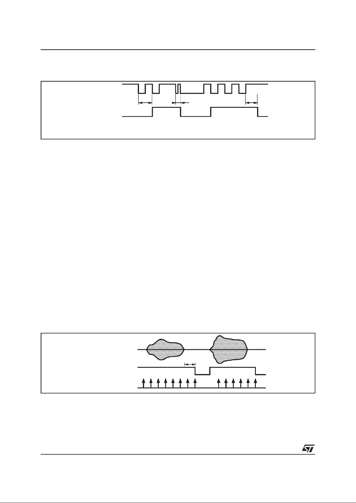
V.3.9 - Ring Detector
This detector detects RING signal from 15Hz to
68Hz, it can be programmed to expand the minimum and maximum detection frequency up to
12Hz(formin)and 144Hz (formax). The detection
time is equal to one period of the ring signal, and
theloosetimeto the minimum between oneperiod
of the ring signal and the inverse of the minimum
frequency.
Theassociated STA_RINGstatus is asFigure 1.
13/84
ST75C530- ST75C540
V - FUNCTIONALDESCRIPTION (continued)
Figure1
RING
T1
STA_RING
1/Fmax prog. < T1< 1/Fmin prog.
T2 < 1/Fmaxprog.
T3
1/Fmin prog.
≈
T2 T3
75C53005.EPS
V.3.10 - VOCODER Description
The Vocoder mode allows the implementation of
an answering machine function. In the CODER
mode the received samples from one of the two
analog inputs, Line or Audio, are compressedby
the ST75C530/540and written into the dual port
RAM Vocoder Buffer (VOCxxx). At the same time
the ST75C530/540 is looking for an incoming
DTMFtone and 4 different programmabletones.
In the DECODER mode thecompressedsamples
are read from the dual port RAM, decompressed
and transmitted to one of the two analog output,
Line or Micx. The ST75C530/540 synthesises an
estimation of its echo and subtracts it from the
received signal. At the same time the
ST75C530/540 is looking for an incoming DTMF
tone and 4 differenttones.
Twoalgorithmsof voicecoding are implemented:
- Low bitrate speech coder (4800bps or 5300bps
with forwarderrorcorrection).
- ADPCM (STproprietaryalgorithm)at 32, 24 and
16Kbps.
If the low bit rate coder algorithm is selected the
ST75C530/540has the capability to slow down or
speed up the DECODER flow up to
±50%. This
Figure2
functionallows a quick message listening if speed
up is used,or at the opposite if slowdown is used,
an enhancementof the voice intelligibility.
V.3.11- VoiceActivity Detector (VAD)
In CODER Mode, for both of the Voice Coding
algorithms, a Voice Activity Detector is implemented while coding by the ST75C530/540. The
STA_109 bit and STA_109Fbit reflect thestate of
the VAD.After the CONF command the VADis on
(assume voice). The default time-out to detect silenceis2 secondsandtheset-uptimeto detectthe
voiceis 15ms. This VADinformationis alsocopied
into the Receive Buffer Status Word MSB (VOCSTA bit7). This detector is fully programmable in
levelsensitivity(down to -60dBm),hysteresis, and
variouscriteria.
An optional silence suppressor is implemented in
the Coder section to suppress long silence in the
incoming message. When enabled (CONF_SUPSILequal1) if a long silenceis detected(STA_109
equal0) theST75C530/540stopsgeneratingBuffer Interrupts.After that if a voiceis againdetected
theST75C530/540will resume the BufferInterrupt
mechanism.
14/84
Rx Signal
STA_109
(or VOCSTA bit 7)
Interrupt (IT1)
2s
75C53006.EPS
V - FUNCTIONALDESCRIPTION (continued)
V.3.12 - TelephonyFunctions
ST75C530/540 telephony software provides both
handset and handsfree modes. ST75C530/540is
connected to the phone line through a D.A.A.,
handset and loudspeaker are connected to
ST75C530/540through amplifiers.
Though the D.A.A. hasto comply withmodem/fax
regulationsin most of the applications,the microphone and the earphone amplifier gains will be
adjustedin compliance with the telephony regula-
Figure3 : Handset/HandsfreeMode Operation
ST75C530- ST75C540
tions.Thesoftwareimplementedin ST75C530/540
allows functionssuch as softclipping,AGC in both
modes,andfullduplexmodein handsfree(seeFigure 3).
V.3.12.1 - HandsetMode
In handsetmode, all the attenuations(_SPKGAIN,
_TXGAIN, _MIKGAIN) are f rom 0dB to -inf
(32768steps).AGC andsoftclipping functions can
beenabledanddisabledbysoftware(seeFigure4).
CODER
AGC
DUAL
RAM
INTERFACE
2 TONE
DETECTORS
AGC
Figure4 : HandsetMode
MIC2
SPK2_1
SPK2_2
2 TONE
GENERATOR
DG
HANDSFREE/
HANDSET
ALGORITHMS
_MIKGAIN
_SPKGAIN
ATT_TX
ATT_MIC
AGC= F(I
Softclipping
AGC= F(I
ADC
ADC
LINE
LINE
DAC
)
)
MUTEDAC
MUTE
[0..-30]dB
Step 3dB
_TXGAIN
DP_RING
RxA
MUTE
MUTE
TxA1
TxA2
TxA1
15
14
TxA2
11
RxA
1
2
SPK1
76
SPK3
77
78
79
SPK2
9
MIC2
8
MIC1
10 MIC3
HYBRID
Line
75C53007.EPS
75C53008.EPS
15/84
ST75C530- ST75C540
V - FUNCTIONALDESCRIPTION (continued)
Tx Characteristics
Symbol Parameter Test Conditions Min. Typ. Max. Unit
Gtx Transmit Gain _MIKGAIN=7FFF,_TXGAIN=7FFF, AGC disabled
Ntx Transmit noise 2kΩbetween MIC2 and GND -73 dBmp
Mmic Microphone mute V
VLpeak Transmit softclipping
level on TxA1-TxA2
Dtx Transmit distortion _MIKGAIN=7FFF,_TXGAIN=7FFF, AGC disabled
MIC2
_MIKGAIN=7FFF,_TXGAIN=7FFF, AGC disabled
see Figure 3, V
see Figure 3, V
= -21dBV
V
MIC2
= -9dBV
V
MIC2
= -21dBV 60 dB
= -9dBV
MIC2
= -9dBV
MIC2
Rx Characteristics
Symbol Parameter Test Conditions Min. Typ. Max. Unit
Grx Receive Gain _SPKGAIN=7FFF,AGC disabled, V
Nrx Receive noise -79 dBmp
Mrx Mute V
Dtx Receive distortion
(SPK2 output)
= dBV 60 dB
RXA
_SPKGAIN=7FFF,AGC Disabled,V
= -16 dBV 6 dB
RXA
= -16dBV 2 %
RXA
18
8
2.5 Vpp
2%
dB
dB
AGC
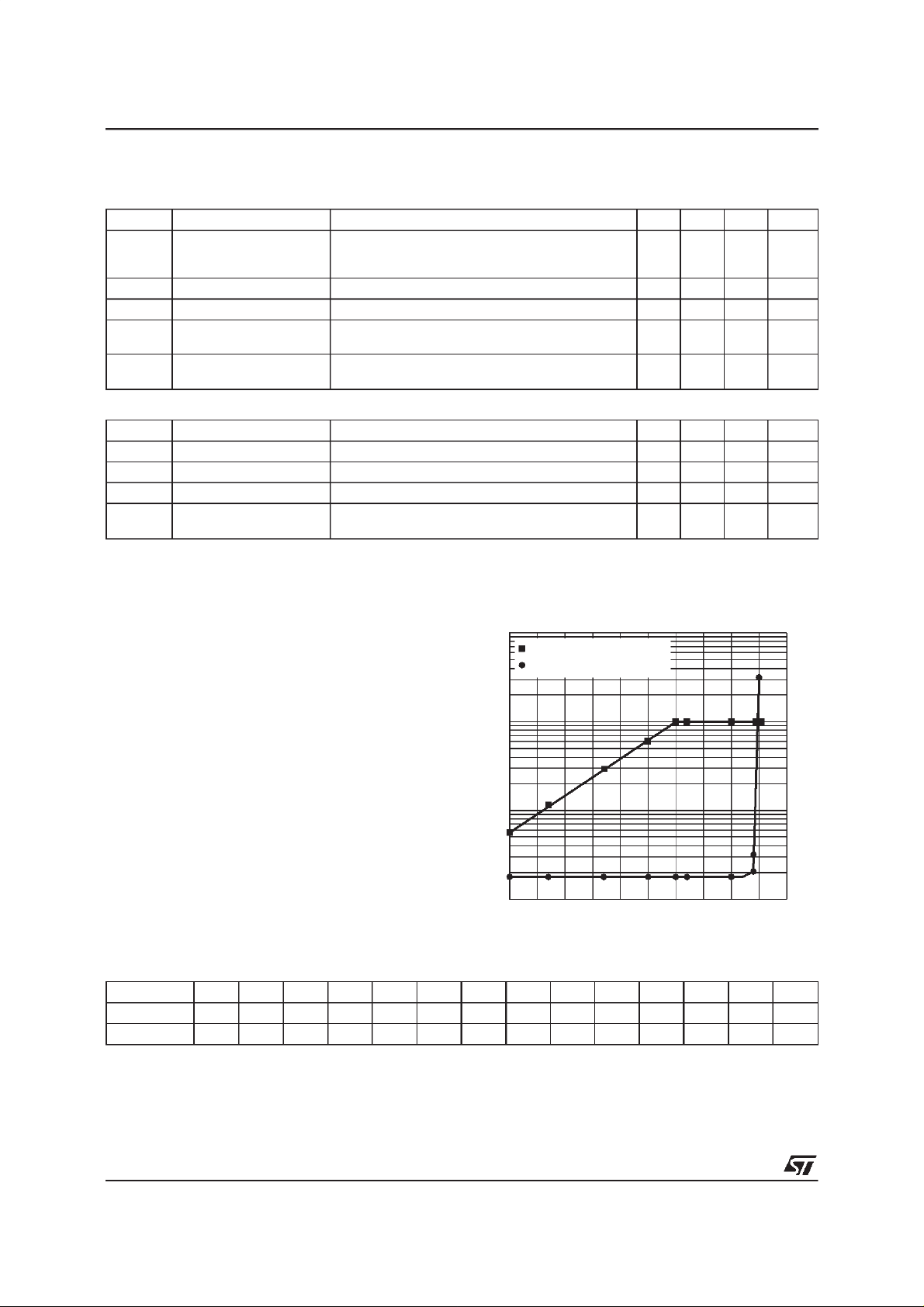
The line current information is coming from the
D.A.A.onDP_RINGpin (frequencycoded information using by example a TS555 general purpose
timer).The AGChas a 6dBdepth. Theattenuation
table can be loaded to comply with each country
regulation.Thedefault table has the followingval-
Figure 5 : SoftclippingStatic Gain
Tx Softclipping and Distortion
(mV
10
) D(%)
RMS
4
VTxA1-TxA2(V
RMS
)
Distortion
ues. The value of the AGC gainis applied to both
Txand Rx path(see Table1).
3
The address of the table is given in the register
10
@_TABLE.
The table length is 53. The AGC is enabled using
CONF or MODC command (see paragraph ”VII COMMANDSETDESCRIPTION”.
Oncethe AGCisrunning,it ispossibletofreezethe
10
2
AGC gain with the register AGC_FRZ.
Softclipping
Thesoftclippingintroducesa 12dBgainand has a
18dBdepth.
The sof tclipp ing value is half digital range
(4000 Hex) (see Figure 5).
10
V
MICX
10
(mV
2
)
RMS
10
Table 1 : AGCGain versus PeriodInformation
Period (ms) <9 10 10.8 11.6 14.5 13.3 14.1 15.5 16.6 17.5 18.3 19.1 20 >20
Table Index <13 13 14 15 16 17 18 19 20 21 22 23 24 >24
Gain (dB) 0 0.7 1.5 2.2 3 3.4 4 4.5 4.8 5.1 5.4 5.6 5.8 6
12
10
8
6
4
2
0
3
75C53009.EPS
16/84
ST75C530- ST75C540
V - FUNCTIONALDESCRIPTION (continued)
V.3.12.2- HandsfreeMode
The handsfree uses a MIC1 and a SPK1 as microphone and loudspeaker interface (see Figure 6).
Figure6 : HandsfreeMode: Full Duplex
MIC1
SPK1P
SPK1N
_MIKGAIN
_SPKGAIN
+
-
ADAPTIVE
FIR
FILTER
ACOUSTIC
FILTER
NLMS
Softclipping
ATTENUATOR
CONTROL
AGC = F(I
ADAPTIVE
NLMS
)
L
AGC = F(I
ADAPTIVE
ATTENUATOR
L
ADAPTIVE
FILTER
)
_TXGAIN
TxA1
TxA2
FIR
RxA
+
Tx Characteristics
Symbol Parameter Test Conditions Min. Typ. Max. Unit
Gtx Transmit Gain _MIKGAIN=7FFF,_TXGAIN=7FFF ,AGCdisabled,
= -21dBV
V
MIC1
24 dB
Ntx Transmit noise 2kΩbetween MIC1 and GND -70 dBmp
Mmic Microphone mute V
Dtx Transmit distortion _MIKGAIN=7FFF,_TXGAIN=7FFF,AGC disabled,
= - dBV 60 dB
MIC1
= -9dBV
V
MIC1
2%
Rx Characteristics
Symbol Parameter Test Conditions Min. Typ. Max. Unit
Grx Receive Gain _SPKGAIN=7FFF, AGC disabled, V
Mrx Mute 60 dB
Dtx Receive distortion
_SPKGAIN=7FFF, AGC disabled, V
(SPK1 output)
= -33dBV 24 dB
RXA
= -33dBV 2 %
RXA
75C53010.EPS
AGC
TheAGC hasthe samebehaviorasin Handsetmode.Furthermore,the maximumgainadded by AGCcan
be fixed by using the RX_GAINMAXand TX_GAINMAXregisters.
Softclipping
SeeFigure 7.
SystemStability
Parameter Test Conditions Min. Typ. Max. Unit
Loop attenuation in Rx RxA to TxA1-TxA2 Speaker gain is12dB, Mike gain is14dB 20 dB
Loop attenuation in Tx MICx to SPK1P-SPK1N Analogique sidetonenot used
20 dB
(see DAA schematics)
It is possible to add some gain switching in the Tx and Rx path (to reduce the gain of the loop) by using
the GAIN_RCV and GAIN_XMTregisters.
17/84
ST75C530- ST75C540
V - FUNCTIONALDESCRIPTION (continued)
Figure7 : SPK1Distortion versusRxA
Rx Softclippingand Distortion
(mV
10
10
10
Figure8 : Speakerand LineTxPower Spectrums
Fxd Y O
Note : Acoustic echo from speaker to microphone input with no
) D (%)
RMS
3
2
VSPK1 (V
RMS
)
Distortion
2
10
(mV
V
MIC2
POWER SPEC1
POWER SPEC2
0.0
0.0
dBm
RMS
V2
dB
RMS
Vv2
-80.0
-80.0
local speech. Receiving speechon line input.
64Avg
64Avg
Speaker Output
Line Tx
)
RMS
0%Ovlp
0%Ovlp
Hz 5k
Ftop
Ftop
10
12
10
8
6
4
2
0
3
V.3.13 - Low Power Mode
Sleepstatecanbeattainedby aSLEEPcommand.
Whenin sleepmode,thedualportRAMis unavailable and the clocksare disabled.
When entering the low power mode, the
ST75C530/540stopsits oscillator,all theperipheralsof theDSPcore arestoppedin orderto reduce
the power consumption. The dual port RAM is
madeinaccessible.
The ST75C530/540can be awakenedby a hardware reset,a RINGsignal or a dummywrite atany
locationin the dual portRAM.
There is a maximum time of 20ms to restart the
oscillator after waking up and an additional 5ms
after the interrupt to be able to accept any commandcoming from the host.
V.3.14 - Reset
After a hardware reset, or an INIT command, the
ST75C530/540 clears all its internal memories,
clearsthe wholedual port RAM andstarts to initialize the delta sigma analog converters.As soon as
75C53011.EPS
these init ializations are complete d, t he
ST75C530/540 generates an interrupt IT6 (commandacknoledge)andis programmedtosendand
receivetones,thesampleclockare programmedto
9600Hz.Thetotal durationofthe resetsequenceis
about 5ms. After that time the ST75C530/540 is
readytoexecutecommandssentbythehostmicrocontroller.Thedurationoftheresetsignalshouldbe
greaterthan700ns.
V.4- Modem Interface
V.4.1 - AnalogInterface
Referto BlockDiagram on page 7.
V.4.2 - General I/O and Relay Interface
16 pins are dedicatedto the generalI/O port. Two
75C53012.EPS
arededicatedto Relaydriver.Theequivalentschematic is as follows: seeFigure 9.
Figure9
IODIR0[x]
IODATA0[x]
IODATA0[x]
18/84
(write)
(read)
GIO0[x]
QD
IORELAY[y]
(write)
QD
RELAY[y]
N
IORELAY[y]
(read)
RGND
75C53013.EPS
V - FUNCTIONALDESCRIPTION (continued)
V.4.3 - Crystal
The crystal frequency must be 44.2368MHz for
ST75C530and 49.152MHzfor ST75C540withan
accuracybetterthat±100 ppm. When using a third
harmoniccrystal the schematicmust beas follow:
seeFigure 10.
Thecrystal featuresare :
- third harmonic,
- parallel, loadcapacitance= 10pF,
- æ 100ppm from 0
<50Ω,
-R
S
o
Cto70oC,
- ATcut(example : SM55-10 MATEL).
Figure10
ST75C540
EXTALL XTALL
*
**
XTAL H3: 44.2368MHz (ST75C530)
73 72
XTAL H3 **
C2
27pF
COG
C1
10pF
COG
Wire wound inductor recommanded (Example : SIGMA-SC30)
Thrird harmonic (Example : MATEL-SM55-10)
49.152MHz(ST75C540)
L*
H (ST75C530)
0.82
µ
0.68µH(ST75C540)
Cb
10nF
V.4.4 - TypicalApplicationSchematic
TheFigure 11is a blockdiagramdesignedtoallow
transmission of fax signals up to +0dBmand sine
waveup to +6dBmon the telephoneline. It allows
receptionoffaxsignalsupto0dBmandsinewaves
upto +6dBm.Figure12isablockdiagramdesigned
ST75C530- ST75C540
to allow transmission of Modem signal up to 10dBmand receptionup to -10dBm.TheOPAmps
are +12/0V powered. With this application schematictheoutofbandtransmitspectrum(from4kHz
to 50kHz) is below-72dBm.
Figures13and14areexamplesofapplicationschematicswhichrespectsgainvalue(respectivelyforfax
and voice application and for Modem application)
andtheminimumdifferentialloadonTxA1andTxA2.
V.4.5 - Host Interface
Thehost interface is seen by the microas a 128x8
RAM, withadditional registers accessiblethrough
an8-bit address space. Aselection Pin (INT/MOT)
allowsto configurethe hostbus foreither INTELor
MOTOROLAtype control signals.
Figure 11
Figure 12
75C53014.EPS
TxA1
TxA2
RxA
V
CM
TxA1
TxA2
RxA
V
CM
2.2nF
2.2nF
+8dB
-10dB
0dB
0dB
600
Ω
-1/2
600Ω 1:1
-1/2
1:1
Line
75C53015.EPS
Line
75C53016.EPS
19/84
ST75C530- ST75C540
V - FUNCTIONALDESCRIPTION (continued)
Figure13 : FaxMode
56.2kΩ 1%
270pF
18.2kΩ 1%
TxA1
TxA2
470nF
470nF
18.2kΩ1%
470pF
+12V
GND
47.5kΩ
560Ω
470nF
30kΩ 1%
1:1 *
22nF
RxA
VCM
Figure14 : DataMode
470nF
TxA1
TxA2
470nF
RxA
VCM
1.2kΩ
2.2nF
18.2kΩ 1%
18.2kΩ 1%
470pF
1.2kΩ
2.2nF
+6V+6V
+6V+6V
+12V
GND
10kΩ 1%
24kΩ 1%
270pF
GND
47.5kΩ
+12V
GND
+12V
6.21kΩ 1%
+6V
24.3kΩ 1% 470nF
560Ω
470nF
30kΩ 1%
6.21kΩ 1%
+6V
24.3kΩ 1%
470nF
+6V +6V
* Insertion loss = 2.5dB between 0 and 3.4kHz
+6V +6V
+6V470nF
1:1 *
22nF
+6V470nF
75C53017.EPS
20/84
33kΩ 1%
* Insertion loss = 2.5dB between 0and 3.4kHz
75C53018.EPS

VI- USER INTERFACE
VI.1- Dual Port Ram Description
The dual port RAM is the standard interface between the hostcontroller and the ST75C530/540,
for either commandsor data. This memory is addressedthrougha7-bitaddressbus. The locations
from$00 to $3Fare RAM location,while locations
from $40 to $60 are control registers dedicatedto
the interrupt handling and the generalIO port and
Relayoutput.
Severalfunctionalareasaredefinedin thedualport
RAMmapping :
- the commandarea,
- the report area,
- the status area,
- the optionalstatus area,
- the data bufferarea,
- the interruptcontrol area,
- the generalI/Oand Relay Outputarea.
VI.1.1 - Mapping
VI.1.1.1- CommandArea
The command area is located from $00 to $04.
Address $00 holds the command byte COMSYS,
and the next four locations hold the parameters
COMPAR[0..3].Thecommandparametersmustbe
enteredbeforethecommandwordis issued.Once
thecommandhasbeenentered,thecommandbyte
isresetandanacknowledgereportisissued.Anew
command shouldnot be issuedbeforetheacknowledgecounterCOMACK is incremented.
VI.1.1.2- Report Area
The report area is located from address $05 to
address$07. Location$05holdstheacknowledge
counter COMACK. Each time a command is acknowledged, the report bytes COMREP[0..1] (if
any) are written by the ST75C530/540 into locations$06 and$07, and the content ofCOMACKis
incremented. This counter allows the
ST75C530/540 to accurately monitor the commandprocessing.
VI.1.1.3- Status Area
Thestatusareaislocatedfromaddress$08to$0B.
TheerrorstatuswordSYSERRislocatedat address
$08.Thiserrorstatuswordisupdatedeachtime an
errorconditionoccurs. An optionalinterruptionIT0
mayadditionallybetriggeredinthe caseofanerror
condition. Locations$09 and $0A hold the general
statusbytesSTATUS[0..1].Themeaning ofthebits
dependsonthemodeof operation,andisdescribed
inChapter VIII.The thirdbyteat address$0B holds
theQualityMonitorbyte STAQUA.
ST75C530- ST75C540
VI.1.1.4- OptionalStatus Area
The user can program (through the DOSR command) the four locations STAOPT[0..3]of the Optional Status Area ($0C to $0F) for the real time
monitoring of fourarbitrary memory locations.
VI.1.1.5- Data Buffer Area
The data area is made of four 8-byte buffers
(see ParagraphVI.1.3“Host InterfaceSummary”).
Two are dedicated to transmission and the two
others to reception. Each of the four buffers is
attachedto astatusbyte.the meaningof thestatus
byte depends on the selected format of transmission. Within eachbuffer,D0 representsthe firstbit
in time.
VI.1.1.6- VOCODERBuffer Area
(VOCODERMode)
Thisareais made ofa 18+2byte buffer.Thisbuffer
contains the VOCODER frame. The first 18 bytes
VOCDATAcontain the coded frame and the other
2 bytes VOCCORR the Error corrections bit (only
valid in low bit ratemode).
In theReceiveMode (CODER)the ST75C530/540
codesthe received samplesand writes the correspondingbytes in thebuffer.If thelow bitratemode
is selected,the ST75C530/540computesthe Error
corrections2 bytesand writesthem in the buffer.
In the Transmit Mode (DECODER) the
ST75C530/540reads the 18codedbytes decodes
themand sendsthe signaltothe analogoutput.In
the low bit rate mode if the Error Correction is
enabled, prior the decoding, the ST75C530/540
reads the 2 Error Correction Bytes and, if any,
correctsthe first 18 bytes.
A mechanism of flags to share the buffer access
betweentheST75C530/540and thehostcontroller
is controlledby the VOCSTAbyte :
- In CODER mode, when the ST75C530/540 has
finis-hed writing the VOCDATA and VOCCORR
bytes, it writes$14 in VOCSTAand generate an
InterruptIT1. The host must read the Data buffer
then clear the VOCSTAbyte.
- In DECODER mode, the host must feed the
VOCDATAand, optionaly,the VOCCORRbytes,
then write $14 (if lowbit rate) or$12 (if ADPCM)
in VOCSTA. The ST75C530/540 will read the
VOCDATA and VOCCORR bytes, clear the
VOCSTA and generate an Interrupt IT1. A silence frame can be generated, in either low bit
rate or ADPCM mode, by writing 00 in all the
VOCDATAbuffer, including the Error Correction
Bytes VOCCORR.
21/84

ST75C530- ST75C540
VI - USER INTERFACE (continued)
VI.1.1.7- InterruptControlArea
Theinterrupt area, that start afterthe address$40
controls the behaviour of the Interrupts mechanism. Register ITSRCR definesthe source of the
interrupt,the registerITMASK allowsindependent
enabling or disabling of any of the interrupt’s
source, registers ITREST0 to ITREST6 reset the
correspondinginterrupt source.
Theseregistersarenotaffectedby aINITcommand,
theyareonlyresetedbya Hardware RESETsignal.
VI.1.1.8- GeneralIO and RelayOutput Area
A set of 5 registers is directly accessible by the
controller to program the General IO pins and
Relay Outputs (see Paragraph VI.1.3 “Host Interface Summary”). Two registers IODIR0 and IODIR1 define the type of the IO pin, either Input or
Output (0 = input, 1 = output), and two registers
IODATA0and IODATA1 define the IO pin signals.
The fifth registerdefines the Relay output signals.
Theseregistersarenotaffectedby aINITcommand,
theyareonlyresetedbya Hardware RESETsignal.
The general IO are setup as input after the power
up or an hardware RESET. The relay output are
openafter powerup or an hardware RESET.
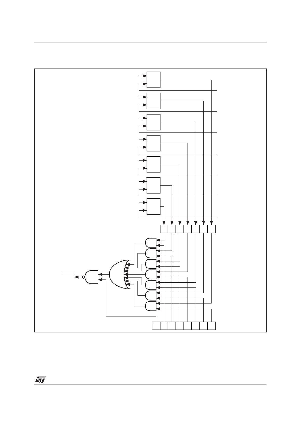
VI.1.2- Interruptions
The ST75C530/540 can generate 7 interruptsfor
the controller. The interrupt handling is made with
a setof registerslocatedfrom $40 to $5F.
The interruptions generated by the ST75C530/540
come from several sources. Once the
ST75C530/540raisesan interrupt,a signal(SINTR)
is sent to the controller. The controller has thento
processtheinterruptandclearit.Theinterruptsource
can be examined in the interrupt source register
ITSRCR located a $50. According to the ITSRCR
bits, the interrupt source can be determined. Then
writing a zero at one of the memorylocation$40 to
$46 (Reset InterruptRegister ITRES[0..6]) will reset the correspondinginterrupt (and thus acknowledgeit).The sourceoftheinterruptcanbe masked
globally or individually using the Interrupt Mast
register ITMASK located at $4F.
Theinterrupt sources are :
- IT0 : Error
This signifiesthat an error has occurred and the
error code is available in the error status byte
SYSERR.Thisbytecanbe selectivelyclearedby
the CSE command.
- IT1 : VOCODERBuffer
Each time the ST75C530/540 have coded a
frame (CODER Mode) or decodeda frame (DECODERMode) this interrupt is generated.
- IT2 : TxBuffer
Each timethe ST75530/C540freesa databuffer,
this interruptis generated.
- IT3 : Rx Buffer
Each time the ST75C530/540 has filled a data
buffer,this interrupt is generated.
- IT4 : StatusByte
This signifies that the status byte has changed
and must be checkedby thecontroller.
- IT5 : Low Power Mode
TheST75C530/540hasbeenawakenedfromthe
low power mode by a low level on theRING pin
or a dummywrite issued bythe host.
- IT6 : CommandAcknowledge
This signifies that the ST75C530/540 has read
the last command entered by the host, incremented the command counter COMACK, and is
readyfora new command.
Note: Interrupt registers are clearedaftera Hardware RESET. These registers are not affectedby
a INIT Command.
22/84
VI- USER INTERFACE(continued)
Figure15 : FunctionalSchematic
ST75C530- ST75C540
ITREST 0
(write only)
ITREST 1
(write only)
ITREST 2
(write only)
ITREST 3
(write only)
ITREST 4
(write only)
ITREST 5
(write only)
ITREST 6
(write only)
R
Q
S
IT0 : Error
R
Q
S
IT1 : VOCODER
R
Q
S
Buffer
IT2 : Tx Buffer
R
Q
S
IT3 : Rx Buffer
R
Q
S
IT4 : Status
R
Q
S
IT5 : Low Power
R
Q
S
IT6 : Command
SINTR
(open drain)
ITSRCR
(read only)
ITMASK
(read write)
0123456
01234567
75C53019.EPS
23/84
ST75C530- ST75C540
VI - USER INTERFACE (continued)
VI.1.3- Host Interface Summary
Address (hex) Description Size (Byte) Mnemonic
COMMAND AREA
$00 Command 1 COMSYS
$01-$04 Command Parameters 4 COMPAR[0..3]
REPORT AREA
$05 Acknowledge Counter 1 COMACK
$06-$07 Report 2 COMREP[0..1]
STATUS AREA
$08 Error Status 1 SYSERR
$09-$0A General Status 2 STATUS[0..1]
$0B Quality Monitor 1 STAQUA
$0C-$0F Optional Report 3 STAOPT[0..3]
DATA BUFFER AREA (FAX Modes andData Modes)
$1C Data Rx Buffer 0 Status 1 DTRBS0
$1D-$24 Data Rx Buffer 0 8 DTRBF0[0..7]
$25 Data Rx Buffer 1 Status 1 DTRBS1
$26-$2D Data Rx Buffer 1 8 DTRBF1[0..7]
$2E Data Tx Buffer 0 Status 1 DTTBS0
$2F-$36 Data Tx Buffer 0 8 DTTBF0[0..7]
$37 Data Tx Buffer 1 Status 1 DTTBS1
$38-$3F Data Tx Buffer 1 8 DTTBF1[0..7]
VOCODER BUFFER AREA (VocoderMode)
$1C Vocoder Buffer Status 1 VOCSTA
$1D-$2E Vocoder Buffer Data 18 VOCDATA
$2F-$30 Vocoder Buffer Corrector 2 VOCCORR
INTERRUPT AREA
$40-$46 Reset Interrupt Register 7 ITREST[0..6]
$4F Interrupt Mask Register 1 ITMASK
$50 Interrupt Source Register 1 ITSRCR
GENERAL IO AND RELAY
$60 I/O Direction 0 1 IODIR0
$61 I/O Direction 1 1 IODIR1
$62 I/O Data 0 1 IODATA0
$63 I/O Data 1 1 IODATA1
$64 I/O Relay Register 1 IORELAY
Note : Registers which address is higheror equal to $40 are not affectedby a INIT Command or a Low Power wake-up. They are reseted
only by a HardwareRESET.
24/84

VI - USER INTERFACE (continued)
VI.2 - CommandSet
The Command Set has the following attractive
features:
- user friendlywith easyto remembermnemonics,
- possibility of straightforwardexpansionwith new
commands to suit specific customer requirements,
- easy upgrade of existingsoftwareusingprevious
modembased SGS-THOMSONproducts.
Thecommandsethasbeendesignedtoprovidethe
necessaryfunctionalcontrolon theST75C530/540.
Eachcommand is classifiedaccordingto its syntax
and the presence/absence of parameters. In the
case of a parametriccommand, parameters must
first be written into the dual port RAM before the
command isissued.Acknowledgeand errorreport
isissuedfor each commandentered.
VI.2.1- CommandSet Summary
VI.2.1.1- OperationalControl Commands
INIT Initialize. Initialize the modem engine.
Setall parameterstotheirdefaultvalues
and wait for commands of the control
processor.Non parametric command.
IDT Identify.Returnthe productidentification
code. Non parametriccommand.
SLEEP Turn to low power mode, the
ST75C530/540 enters the low power
mode and stops its crystal oscillator to
reducepowerconsumption.Inthismode
all the clocks are stopped and the dual
RAM is unreachable.
HSHK Handshake. Begins the handshake
sequence.Themodemenginegenerates
all the sequences defined in the ITU-T
recommendations. A status report
indicatesto thecontrolprocessorthestate
of the handshake. This command only
applies to modes where a handshake
sequence is defined.A CONFcommand
musthavebeen issuedpriorto theuseof
HSHK. Nonparametriccommand.
STOP FAX Sto p. Stop FAX Half-duplex
transmitter.Non parametric command.
RTRA Retrain. Begin a retrain sequence in
V.32bis/V.32 or V.22bis modes as
described in the ITU-T
recommendations(ST75C540only).
ST75C530- ST75C540
SYNC FAXSynchronize.Start/StopofFAXHalf-
duplexreceiver. Parametriccommand.
CSE Clea rStatu sEr r o r.Selectivelyclear stheError
statusbyteSYSERR.Par a m etri ccomman d.
SETGN Set Gain.This command sets theglobal
gainfactor,whichis usedforthetransmit
samples.Parametriccommand.
VI.2.1.2- Data CommunicationCommands
XMIT Transmit Data. Start/stop the
transmission of data. After a XMIT
command,theST75C530/540sendsthe
data contained in its dual port RAM.
FORM Selects the Transmission Format. This
command configures the data interface
for both re ceiver and transmitte r
according to the selected data format.
Parametric command (HDLC, UART or
synchronous).
VI.2.1.3- MemoryHandlingCommands
MWI
MWLO
MW
MRI
MRLO
MR
CR Complex Read. This command allows
MemoryWrite Indirect
MemoryWrite Low Word
MemoryWrite.This commandis usedto
write an arbitrary 16-bit value into the
writable memory lo cation currently
specified by a parameter. Parametric
command.
MemoryRead Indirect
MemoryRead Low Word
MemoryRead.Thiscommandallowsthe
controller to read any of the ERAM or
CROM (ST75C530/540 memory
spaces)locationwithout interrupting the
processor. Parametric command.
the controller to read at the same time
the realand imaginary partof acomplex
valuestoredinadoubleERAMor
CROM location. This feature is very
interesting for eye pattern software
control and for equalization monitoring.
This commandinsures that the real and
imaginary parts are sampled in the
memory at the same time (integrity).
Parametric command.
25/84
ST75C530- ST75C540
VI - USER INTERFACE (continued)
VI.2.1.4- Configuration Control Commands
ASEL Select the Analo g path option, like
Microphone input, Speaker attenuation.
Parametriccommand.
CONF Configure. This commandconfiguresthe
modemengine fordatatransmissionand
handshakeprocedures (if any) in any of
the supported modes. The transmission
parametersare set totheirdefaultvalues
and can be modified with the MODC
command.Parametric command.
MODC Modify Configuration. This command
allows mod ification of some of th e
parameters which have been set up by
theCONF command.It canalso be used
to alter the mode of operations (short
train).Parametriccommand.
DOSR Define Optional Status Report. This
command allows the modification of the
optionalstatusreportlocatedinthestatus
areaof the dualport RAM. One can thus
select a particular parameter to be
monitoredduring all modes of operation.
Parametriccommand.
DSIT Define Status Interrupt. This command
allows the programming of the status
word bit that will generate an Interrupt to
thecontroller.Parametric command.
VI.2.1.5- Tone Generation Commands
TONE SelectTone .Progr amsthetonegenerator ( s)
for the desired default tone(s ) . Additi onal
mnemonics provide quick progra m m i ng of
DTMF tonesor other currently used tones.
Parametriccommand.
DEFT Define Tone. Programs the tone
generator(s)for arbitrary tone synthesis.
Parametriccommand.
TGEN Tone Generator Control. Enabl es or
disables the tone generator(s).
Parametriccommand.
VI.2.1.6- Tone Detection Commands
TDRC Read Tone Detector Coefficient. Read
one Tone Detect or Coefficient.
Parametriccommand.
TDWC Write Tone Detector Coefficient. Write
one Tone Detect or Coefficient.
Parametriccommand.
TDRW Read Tone Detector Wiring. Read one
Tone Detector Wiring connection.
Parametriccommand.
TDWW Write Tone Detector Wiring. Write one
Tone Detector Wiring connection.
Parametriccommand.
TDZ Clear Tone Detector Cell. Clear internal
variable s of a Ton e Det ect or Ce ll.
Parametriccommand.
VI.2.1.7- MiscellaneousCommands
CALL Call a Subroutine. Call a subroutinewith
one Parameter.Parametriccommand.
JSR Call a Low Level Subroutine. Call an
internal subroutine with one parameter.
Parametriccommand.
VI.3- CommandSet Short Form
CCI Command
Mnemonic Value Description
XMIT 0x01 Transmit Data
SETGN 0x02 Set Transmit Gain
SLEEP 0x03 Power DowntheST75C530/540
HSHK 0x04 FAX Start Transmitter
RTRA* 0x05 Retrain(V.32bis/V.32andV.22bis)
INIT 0x06 Initialize (Software Reset)
CSE 0x08 Clear Error StatusWord
FORM 0x09 Define Data Format
DOSR 0x0A Define Optional StatusReport
ASEL 0x0B Select the Analog Path Options
TONE 0x0C Generate Predefined Tones
TGEN 0x0D Enable Tone Generator
DEFT 0x0E Define Arbitrary Tone
MR 0x10 Memory Read
CR 0x11 Complex Read
MW 0x12 Memory Write
DSIT 0x13 Define Status Interrupt
IDT 0x14 ReturnProductIdentificationCode
JSR 0x18 Call a Low Level Routine
CALL 0x19 Call a Routine
TDRC 0x1A Tone Detector Read Coefficient
TDRW 0x1B Tone DetectorRead Wiring
TDWC 0x1C Tone Detector Write Coefficient
TDWW 0x1D Tone DetectorWrite Wiring
TDZ 0x1E Tone DetectorClear Cell
CONF 0x20 Configure
MODC 0x21 Modify Default Configuration
STOP 0x25 FAX Stop Transmitter
SYNC 0x26 FAX Synchronize Receiver
MRI 0x28 Memory Read Indirect
MRLO 0x29 Memory Read Low Word
MWI 0x2A Memory Write Indirect
MWLO 0x2B Memory WriteLow Word
* ST75C540 only.
26/84
 Loading...