

SGS Thomson Microelectronics ST75C185CTR, ST75C185CN, ST75C185CDR, ST75C185CD, ST75C185BTR Datasheet
...
MULTIPLE RS-232 DRIVERS AND RECEIVERS
■ MEETS STANDAR DEIA-232-E
■
SINGLECHIPWITHINTERFACEBETWEEN
UARTAND SERIALPORTCONNECTOR
■
LESSTHAN 20mW QUIESCENTPOWER
CONSUMPTION
■ WIDEDRIVERSUPPLYVOLTAGE:7TO13.2V
■
DRIVEROUTPUTSLEWRATE LIMITEDTO
30V/µsMAX
■ RECEIVERINPUTHYSTERESIS:1.1TYP
■ PUSH-PULLRECEIVEROUTPUTS
■ ONCHIPRECEIVER1µsNOISEFILTER
■
FUNCTIONALLY INTERCHANGEABLEWITH
STMST75185
■ ESDPROTECTION:
MODEL
DESCRIPTION
The ST75C185 is low power BICMOS device
containing three independent drivers and five
receivers that is used to interface data terminal
equipment (DTE) with data circuit-terminating
equipment (DCE). This device has been
designed to conform to Standards
ANSI/EIA-232-E. The drivers have a controlled
output slew rate that is limited to a maximum of
30V/µs and the receivers have filters that reject
input noise pulses that are shorter than 1µs. Both
±10KVHUMANBODY
ST75C185
LOW POWER
TARGET DATA
(Micro Package)
(PlasticPackage)
(TSSOPPackage)
these features eliminate the need of external
components.
The ST75C185 hasn’t a power sequence fault
condition. It has been designed using low-power
techniquesin a BICMOStecnology.
In most application the receivers contained in this
device will interface to single inputs peripheral
devices such as ACEs, UARTs or
microprocessors. By using sampling, such
peripheral devices are usuallly insensitive to the
transition times of the input signals. If this is not
the case, or for other uses, it is recommended
that the ST75C185 receiver outputs be buffered
by single gates of the HCMOS, ALS or 74F logic
families.
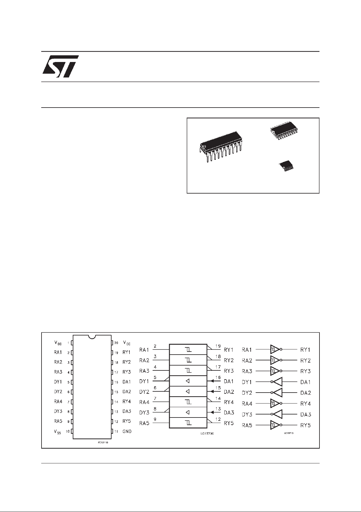
PIN CONNECTION IEC LOGICSYMBOL AND LOGIC DIAGRAM
June 2000
1/13
ST75C185
ORDERCODES
Typ e Temp era t u re Rang e Packag e Commen ts
ST75C185CN 0 to 70
ST75C185CD 0 to 70
ST75C185CDR 0 to 70
ST75C185CTR 0 to 70
ST75C185BN -40to 85
ST75C185BD -40to 85
ST75C185BDR -40 to 85
ST75C185BTR -40 to 85
PIN DESCRIPTION
PIN No SYMBOL NAME AND F UNCTION
1V
2 RA1 First Receiver Input
3 RA2 Second Receiver Input
4 RA3 Third Receiver Input
5 DY1 First Driver Output
6 DY2 Second Driver Output
7 RA4 FourthReceiver Input
8 DY3 Third Driver Output
9 RA5 Fifth Receiver Input
10 V
11 GND Ground
12 RY5 Fifth Receiver Output
13 DA3 Third Driver Input
14 RY4 Fourth Receiver Output
15 DA2 Second Driver Input
16 DA1 First Driver Input
17 RY3 Third Receiver Output
18 RY2 Second Receiver Output
19 RY1 First Receiver Output
20 V
o
C DIP-20 20 parts per tube / 50 tubes per box
o
C SO-20 (Tube) 40 parts per tube / 25 tubesper box
o
C SO-20 (Tape & Reel) 1000 parts per reel
o
C TSSOP20 (Tape & Reel) 2500 parts per reel
o
C DIP-20 20 parts per tube / 50 tubes per box
o
C SO-20 (Tube) 40 parts per tube / 25 tubesper box
o
C SO-20 (Tape & Reel) 1000 parts per reel
o
C TSSOP20 (Tape & Reel) 2500 parts per reel
DD
SS
CC
Supply Voltage (+12V)
Supply Voltage (-12V)
Supply Voltage (+5V)
2/13
ST75C185
ABSOLUTE MAXIMUM RATINGS OVER OPERATING FREE-AIRTEMPERATURE RANGE
(unlessotherwise specified)
Symb o l Parameter Value Uni t
V
V
V
V
V
V
V
I
T
T
T
AbsoluteMaximum Ratingsarethosevaluesbeyond whichdamageto thedevicemayoccur. Functionaloperationunderthesecondition isnotimplied.
NOTE1:All voltages arewithrespect tothenetwork ground terminal.
RECOMMENDED OPERATING CONDITIONS
Symb o l Parameter Mi n TYP Max Unit
V
V
V
V
I
OH
I
T
NOTE 2: The algebraic convertion, where the more positive (less negative) limitis designed as maximum, isused in this datasheet for logic levels only,
e.g.if-10Visa maximum,thetypicalvalueisa morenegativevoltage.
Supply Voltage (Note 1) 15 V
DD
Supply Voltage (Note 1) -15 V
SS
Supply Voltage (Note 1) 7 V
CC
Input Voltage Range (DRIVER) -0.3 to (VCC+0.3) V
I
Input Voltage Range (RECEIVER) -30 to 30 V
I
Output Voltage Range (DRIVER) (VSS-6) to (VDD+6) V
O
Output Voltage Range (RECEIVER) -0.3 to (VCC+0.3) V
O
Receiver Low Level Output Current 20 mA
O
Operating Free-Air Temperature Range -40 to 85
A
Storage Temperature Range -65 to +150
stg
Lead Temperature 1.6mm from case for 10 sec 260
L
Supply Voltage 7 12 13.2 V
DD
Supply Voltage -7 -12 -13.2 V
SS
Supply Voltage 4.5 5 5.5 V
CC
Input Voltage (Note 2) DRIVER 0V
IN
CC
RECEIVER -25 25
High Level Output Current RECEIVER -1 mA
Low Level Output Current RECEIVER 3.2 mA
OL
Operating Free-Air Temperature -40 25 85
A
o
C
o
C
o
C
V
o
C
3/13
ST75C185
SUPPLYCURRENTS
= 12V, VSS= -12V,VCC= 5V, unlessotherwise specified)
(V
DD
Symbol Parameter Test Cond itions Value Uni t
Min. Typ. Max.
Supply Current from V
I
DD
Supply Current from V
I
SS
Supply Current from V
I
CC
DD
SS
CC
No load. All inputs at 2 or 0.8V 115 500
No load. All inputs at 2 or 0.8V -115 -500 µ
No load. All inputs at 0 or 5V 950 1500
A
µ
A
A
µ
DRIVERELECTRICALCHARACTERISTICS OVER OPERATINGTEMPERATURE RANGE
= 12V, VSS=-12V, VCC=5V±10%, unlessotherwise specified)
(V
DD
Symbol Parameter Test Cond itions Value Uni t
Min. Typ. Max.
High Level Output Voltage VIL=0.8V
V
OH
R
=3K
L
Ω
(See Figure 1)
V
Low Level Output Voltage
OL
(Note 3)
VIH= 1.9 V
=3K
R
Ω
L
(See Figure 1)
V
High Level Input Voltage 2 1.4 V
IH
Low Level Input Voltage 1.4 0.8 V
V
IL
High Level Input Current VI= 5 V (See Figure 2) 1 µA
I
IH
Low Level Input Current VI= 0 V (See Figure 2) -1 µA
I
IL
I
High Level Short Circuit
OS(H)
Output Current (Note 4)
I
Low Level Short Circuit
OS(L)
Output Current (Note 4)
Output Resistance VO=-2to2V VSS=VCC=VDD= 0V 300 450
R
O
NOTE3: The algebraic convention, where themore positive (less negative) limit is designated as maximum, isused in thisdatasheet forlogic levels only
(e.g.if-10Visa maximum,thetypicalvalueis a morenegative voltage).
NOTE4: Notmorethanoneoutputs shouldbeshorted atonetime.
VI=0.8V VO=0VorV
(See Figure 1)
VI=2V VO=0VorV
(See Figure 1)
V
= 7V, VSS= -7V 5 6.3 V
DD
= 12V, VSS= -12V 10 10.8 V
V
DD
V
= 7V, VSS= -7V -6.3 -5 V
DD
V
= 12V, VSS= -12V -10.8 -10 V
DD
SS
SS
-6 -20 -60 mA
63560mA
Ω
DRIVERSWITCHING CHARACTERISTICS
= 12V, VSS=-12V, VCC=5V TA=25oC)
(V
DD
Symbol Parameter Test Cond itions Value Uni t
Min. Typ. Max.
Propagation Delay Time, Low
t
PLH
to High Level Output
t
Propagation Delay Time High
PHL
to Low Level Output
Transition Time Low to High
t
TLH
Level Output
t
Transition Time High to Low
THL
Level Output
SR Output Slew Rate (Note 5)
=3to7KΩCL=1000pF
R
L
(See Figures 3)
=3to7KΩCL=1000pF
R
L
(See Figures 3)
=3to7KΩCL=1000pF
R
L
(See Figures 3)
=3to7KΩ CL=1000pF
R
L
(See Figure 3)
R
=3to7K
L
= 50 to 2500 pF
C
L
Ω
0.53 2 3.2
0.53 2 3.2 µs
(See Figure 3)
NOTE5: Measuredbetween-3Vand3Vpointsofoutputwaveform(EIA-232-Econditions), allunusedinputstied eitherhighorlow.
4/13
1.9 4
µ
1.6 4 µs
µ
41130V/
s
s
s
µ

ST75C185
RECEIVERELECTRICAL CHARACTERISTICS OVER OPERATINGTEMPERATURERANGE
= 12V, VSS=-12V, VCC=5V±10%, unlessotherwise specified)
(V
DD
Symbol Parameter Test Cond itions Value Uni t
Min. Typ. Max.
Positive Going Threshold
V
T+
Voltage
Negative Going Threshold
V
T-
Voltage
Input Hysteresis (VT+-VT-)
V
hys
(Note 6)
High Level Output Voltage
V
OH
(Note 7)
Low Level Output Voltage VI=3V IOL=3.2mA
V
OL
High Level Input Current VI= 25 V (See Figure 6) 3.6 4.5 8.3 mA
I
IH
Low Level Input Current VI= -25 V (See Figure 6) -3.6 -4.4 -8.3 mA
I
IL
I
Short-Circuit Output Current
OS(H)
at High Level
I
Short-Circuit Output Current
OS(L)
at Low Level
AlltypicalvaluesareatTA=25oC,
NOTE6: Hysteresis is thedifference between the positive going input threshold voltage, V
NOTE7: Ifthe inputs are letfunconnected, the receiver interprets thisas an input low, and the receiver outputs willremain in the high state.
(See Figure 6) 1.6 2.1 2.55
(See Figure 6) 0.65 1 1.25 V
0.6 1.1
IOH= 0.75mA or Input Open
= -1mA (See Figure 6)
I
OH
3.5 4.8 V
0.2 0.4 V
(See Figure 6)
= 3 V (See Figure 6) 0.43 0.55 1
V
I
= -3 V (See Figure 6) -0.4 -0.55 -1
V
I
VI=0.75V VO=0V
-13 -30 mA
(See Figure 5)
VI=V
CC
VO=V
CC
35 60 mA
(See Figure 5)
, and the negative going input threshold voltage VT-.
T+
V
V
RECEIVER SWITCHINGCHARACTERISTICS
= 12V, VSS= -12V,VCC=5V±10% TA=25oC)
(V
DD
Symb ol Parameter Test Co n d iti ons V al u e Unit
Min. Typ. Max.
Propagation Delay Time, Low
t
t
t
t
t
W(N)
PLH
to High Level Output
Propagation Delay Time High
PHL
to Low Level Output
Transition Time Low to High
TLH
Level Output
Transition Time High to Low
THL
Level Output
Pulse Duration of longest
pulse rejection as noise
=5KΩ CL=50pF
R
L
(See Figure 6)
=5KΩCL=50pF
R
L
(See Figure 6)
=5KΩCL=50pF
R
L
(See Figure 6)
=5KΩ CL=50pF
R
L
(See Figure 6)
=5KΩCL=50pF
R
L
(See Figure 6)
(Note8)
NOTE8:Thereceiverignoresanypositiveor negativegoingpulsethatis lessthantheminimumvalueoft
pulsegreater thanthemaximum oft
W(N)
.
andaccepts anypositiveornegative going
W(N)
3.2 4
2.6 4 µs
30 100 ns
10 50 ns
1 2.3 4
µ
µ
s
s
5/13

ST75C185
APPLICATION CIRCUITS
TTL LEVEL
DCD 38
DSR 37
RXD 21
UART
(16550)
RTS 32
TXD 11
CTS 36
DTR 33
RI 39
To CPU BUS
100nF
Vdd
+12 V
ST75C185
Vcc
20
Rout1
19
Rout2
18
Rout3
17
Din1
16
Din2
15
Rout4
14
Din3
13 8
Rout5
12
GND
11
Vdd
Rin1
Rin2
Rin3
Dout1
Dout2
Rin4
Dout3
Rin5
Vss
1
2
3
4
5
6
7
9
10
Vss
-12V
Vcc
+5 V
100nF
CL
100nF
RS232 LEVEL
PC Serial Port
1
DCD
DSR
RXD
RTS
CL
TXD
CTS
DTR
CL
RI
GND
6
2
7
3
8
4
9
5
DB9S EIA232-E
Serial Port
Connector
FIGURE1: Driver Test Circuit for VOH,VOL,
and I
I
SO(H)
6/13
SO(L)
FIGURE2: Driver Test Circuit for IIHand I
IL

ST75C185
FIGURE3:
DriverTest Circuit
FIGURE5: Receiver Test Circuit for I
OS
FIGURE4:
Driver VoltageWaveforms
FIGURE6: Receiver Test Circuit forVT,VOH,V
OL
FIGURE7: Receiver Test Circuit FIGURE8: Receiver Voltage Waveforms
NOTEA:Thepulsegenerator has thefollowingcharacteristics:t
NOTEB:C
includesprobeandjigcapacitance.
L
=25µs,PRR=20KHz,ZO=50Ω,tr=tf<50ns.
W
7/13

ST75C185
DriverVoltage Transfer Characteristics
DriverShort Circuit OutputCurrent vs Free-Air
Temperature
DriverOutput Current vs OutputVoltage
DeviceSupply Current vs Temperature
ReceiverThresholdvs Temperature
8/13
ReceiverThresholdvs SupplyVoltage

ST75C185
APPLICATION INFORMATION: DIODESON POWER SUPPLY
Diodes placedin serieswith theV
and VSSleads protectthe ST75C185in the fault condition in which
DD
the devices output are shorted to±15V and the power supplies are at low state and provide
low-impedancepath to ground (see Figure below). Any idle transmitterinput mustbe connectedto GND
. This deviceis not sensitiveto power supply sequence.
or V
CC
+Vdd
Output
ST75C185
Output shorted
to ±15V
Output
ST75C185
-Vss
9/13

ST75C185
Plastic DIP-20 (0.25)MECHANICAL DATA
DIM.
MIN. TYP. MAX. MIN. TYP. MAX.
a1 0.254 0.010
B 1.39 1.65 0.055 0.065
b 0.45 0.018
b1 0.25 0.010
D 25.4 1.000
E 8.5 0.335
e 2.54 0.100
e3 22.86 0.900
F 7.1 0.280
I 3.93 0.155
L 3.3 0.130
Z 1.34 0.053
mm inch
10/13
P001J

SO-20 MECHANICAL DATA
ST75C185
DIM.
MIN. TYP. MAX. MIN. TYP. MAX.
A 2.65 0.104
a1 0.10 0.20 0.004 0.007
a2 2.45 0.096
b 0.35 0.49 0.013 0.019
b1 0.23 0.32 0.009 0.012
C 0.50 0.020
c1 45 (typ.)
D 12.60 13.00 0.496 0.512
E 10.00 10.65 0.393 0.419
e 1.27 0.050
e3 11.43 0.450
F 7.40 7.60 0.291 0.299
L 0.50 1.27 0.19 0.050
M 0.75 0.029
S 8 (max.)
mm inch
P013L
11/13

ST75C185
TSSOP20 MECHANICAL DATA
DIM.
mm inch
MIN. TYP. MAX. MIN. TYP. MAX.
A 1.1 0.433
A1 0.05 0.10 0.15 0.002 0.004 0.006
A2 0.85 0.9 0.95 0.335 0.354 0.374
b 0.19 0.30 0.0075 0.0118
c 0.09 0.2 0.0035 0.0079
D 6.4 6.5 6.6 0.252 0.256 0.260
E 6.25 6.4 6.5 0.246 0.252 0.256
E1 4.3 4.4 4.48 0.169 0.173 0.176
e 0.65 BSC 0.0256 BSC
K0
o
o
4
o
8
o
0
o
4
8
L 0.50 0.60 0.70 0.020 0.024 0.028
o
A
PIN 1 IDENTIFICATION
12/13
A2
A1
b
e
K
c
L
E
D
E1
1

ST75C185
Information furnished isbelieved to be accurate and reliable. However, STMicroelectronics assumes no responsibility for the consequences
of use of such information nor for any infringement of patents or other rights of third parties which may result from its use. No license is
granted by implication or otherwise under any patent or patent rights of STMicroelectronics. Specification mentioned in this publication are
subject to change without notice. Thispublication supersedes andreplaces all information previously supplied. STMicroelectronics products
are not authorized for use as critical components in lifesupport devices or systems withoutexpress written approval of STMicroelectronics.
The ST logo is a registered trademark of STMicroelectronics
2000 STMicroelectronics – Printed in Italy – All RightsReserved
STMicroelectronics GROUP OF COMPANIES
Australia - Brazil -China - Finland - France - Germany - Hong Kong - India - Italy- Japan- Malaysia - Malta - Morocco
Singapore - Spain - Sweden - Switzerland - United Kingdom - U.S.A.
http://www.st.com
.
13/13
 Loading...