

SGS Thomson Microelectronics ST75C185CTR, ST75C185CN, ST75C185CDR, ST75C185CD, ST75C185BTR Datasheet
...
MULTIPLE RS-232 DRIVERS AND RECEIVERS
■ MEETS STANDAR DEIA-232-E
■
SINGLECHIPWITHINTERFACEBETWEEN
UARTAND SERIALPORTCONNECTOR
■
LESSTHAN 20mW QUIESCENTPOWER
CONSUMPTION
■ WIDEDRIVERSUPPLYVOLTAGE:7TO13.2V
■
DRIVEROUTPUTSLEWRATE LIMITEDTO
30V/µsMAX
■ RECEIVERINPUTHYSTERESIS:1.1TYP
■ PUSH-PULLRECEIVEROUTPUTS
■ ONCHIPRECEIVER1µsNOISEFILTER
■
FUNCTIONALLY INTERCHANGEABLEWITH
STMST75185
■ ESDPROTECTION:
MODEL
DESCRIPTION
The ST75C185 is low power BICMOS device
containing three independent drivers and five
receivers that is used to interface data terminal
equipment (DTE) with data circuit-terminating
equipment (DCE). This device has been
designed to conform to Standards
ANSI/EIA-232-E. The drivers have a controlled
output slew rate that is limited to a maximum of
30V/µs and the receivers have filters that reject
input noise pulses that are shorter than 1µs. Both
±10KVHUMANBODY
ST75C185
LOW POWER
TARGET DATA
(Micro Package)
(PlasticPackage)
(TSSOPPackage)
these features eliminate the need of external
components.
The ST75C185 hasn’t a power sequence fault
condition. It has been designed using low-power
techniquesin a BICMOStecnology.
In most application the receivers contained in this
device will interface to single inputs peripheral
devices such as ACEs, UARTs or
microprocessors. By using sampling, such
peripheral devices are usuallly insensitive to the
transition times of the input signals. If this is not
the case, or for other uses, it is recommended
that the ST75C185 receiver outputs be buffered
by single gates of the HCMOS, ALS or 74F logic
families.
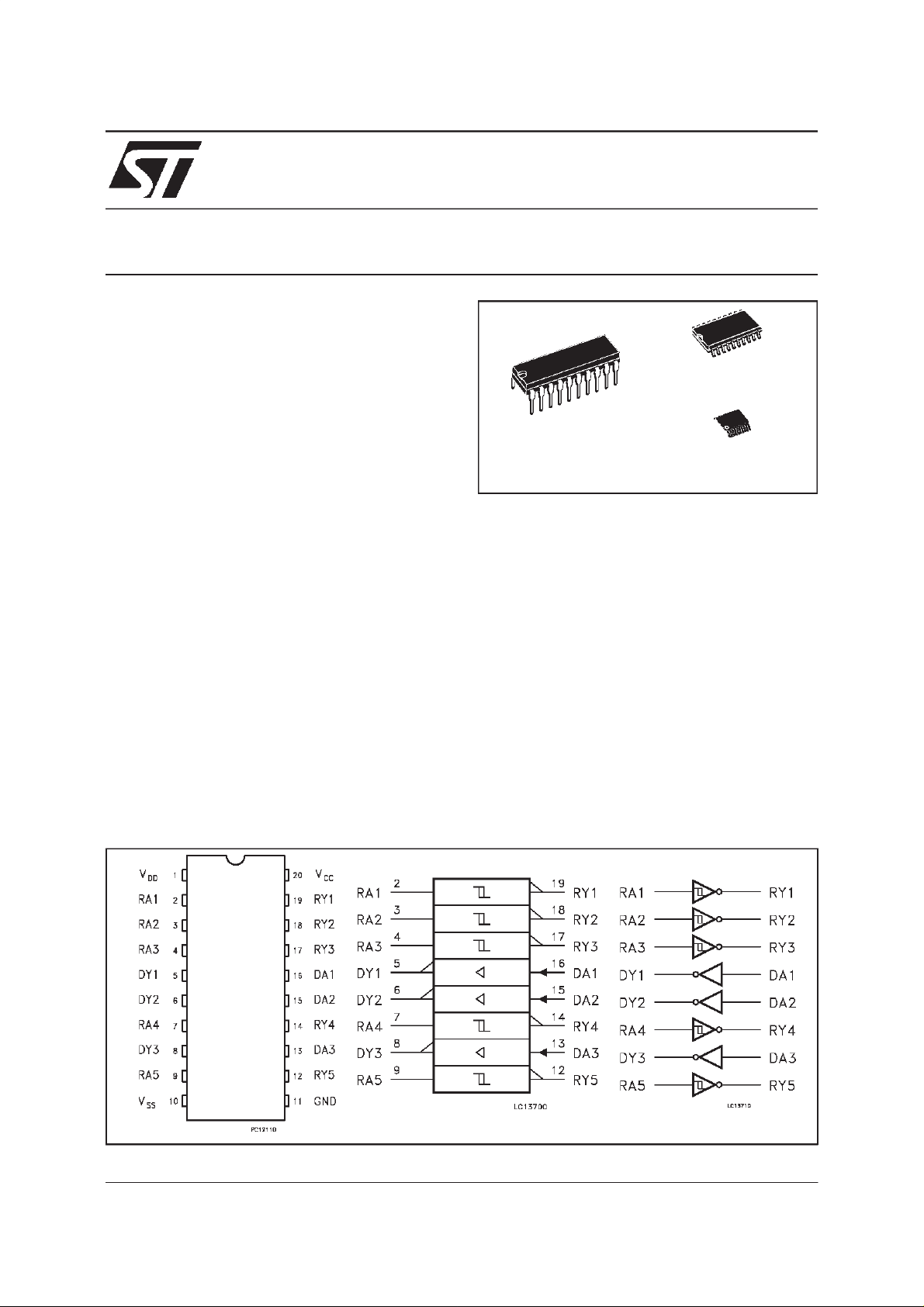
PIN CONNECTION IEC LOGICSYMBOL AND LOGIC DIAGRAM
June 2000
1/13
ST75C185
ORDERCODES
Typ e Temp era t u re Rang e Packag e Commen ts
ST75C185CN 0 to 70
ST75C185CD 0 to 70
ST75C185CDR 0 to 70
ST75C185CTR 0 to 70
ST75C185BN -40to 85
ST75C185BD -40to 85
ST75C185BDR -40 to 85
ST75C185BTR -40 to 85
PIN DESCRIPTION
PIN No SYMBOL NAME AND F UNCTION
1V
2 RA1 First Receiver Input
3 RA2 Second Receiver Input
4 RA3 Third Receiver Input
5 DY1 First Driver Output
6 DY2 Second Driver Output
7 RA4 FourthReceiver Input
8 DY3 Third Driver Output
9 RA5 Fifth Receiver Input
10 V
11 GND Ground
12 RY5 Fifth Receiver Output
13 DA3 Third Driver Input
14 RY4 Fourth Receiver Output
15 DA2 Second Driver Input
16 DA1 First Driver Input
17 RY3 Third Receiver Output
18 RY2 Second Receiver Output
19 RY1 First Receiver Output
20 V
o
C DIP-20 20 parts per tube / 50 tubes per box
o
C SO-20 (Tube) 40 parts per tube / 25 tubesper box
o
C SO-20 (Tape & Reel) 1000 parts per reel
o
C TSSOP20 (Tape & Reel) 2500 parts per reel
o
C DIP-20 20 parts per tube / 50 tubes per box
o
C SO-20 (Tube) 40 parts per tube / 25 tubesper box
o
C SO-20 (Tape & Reel) 1000 parts per reel
o
C TSSOP20 (Tape & Reel) 2500 parts per reel
DD
SS
CC
Supply Voltage (+12V)
Supply Voltage (-12V)
Supply Voltage (+5V)
2/13
ST75C185
ABSOLUTE MAXIMUM RATINGS OVER OPERATING FREE-AIRTEMPERATURE RANGE
(unlessotherwise specified)
Symb o l Parameter Value Uni t
V
V
V
V
V
V
V
I
T
T
T
AbsoluteMaximum Ratingsarethosevaluesbeyond whichdamageto thedevicemayoccur. Functionaloperationunderthesecondition isnotimplied.
NOTE1:All voltages arewithrespect tothenetwork ground terminal.
RECOMMENDED OPERATING CONDITIONS
Symb o l Parameter Mi n TYP Max Unit
V
V
V
V
I
OH
I
T
NOTE 2: The algebraic convertion, where the more positive (less negative) limitis designed as maximum, isused in this datasheet for logic levels only,
e.g.if-10Visa maximum,thetypicalvalueisa morenegativevoltage.
Supply Voltage (Note 1) 15 V
DD
Supply Voltage (Note 1) -15 V
SS
Supply Voltage (Note 1) 7 V
CC
Input Voltage Range (DRIVER) -0.3 to (VCC+0.3) V
I
Input Voltage Range (RECEIVER) -30 to 30 V
I
Output Voltage Range (DRIVER) (VSS-6) to (VDD+6) V
O
Output Voltage Range (RECEIVER) -0.3 to (VCC+0.3) V
O
Receiver Low Level Output Current 20 mA
O
Operating Free-Air Temperature Range -40 to 85
A
Storage Temperature Range -65 to +150
stg
Lead Temperature 1.6mm from case for 10 sec 260
L
Supply Voltage 7 12 13.2 V
DD
Supply Voltage -7 -12 -13.2 V
SS
Supply Voltage 4.5 5 5.5 V
CC
Input Voltage (Note 2) DRIVER 0V
IN
CC
RECEIVER -25 25
High Level Output Current RECEIVER -1 mA
Low Level Output Current RECEIVER 3.2 mA
OL
Operating Free-Air Temperature -40 25 85
A
o
C
o
C
o
C
V
o
C
3/13
ST75C185
SUPPLYCURRENTS
= 12V, VSS= -12V,VCC= 5V, unlessotherwise specified)
(V
DD
Symbol Parameter Test Cond itions Value Uni t
Min. Typ. Max.
Supply Current from V
I
DD
Supply Current from V
I
SS
Supply Current from V
I
CC
DD
SS
CC
No load. All inputs at 2 or 0.8V 115 500
No load. All inputs at 2 or 0.8V -115 -500 µ
No load. All inputs at 0 or 5V 950 1500
A
µ
A
A
µ
DRIVERELECTRICALCHARACTERISTICS OVER OPERATINGTEMPERATURE RANGE
= 12V, VSS=-12V, VCC=5V±10%, unlessotherwise specified)
(V
DD
Symbol Parameter Test Cond itions Value Uni t
Min. Typ. Max.
High Level Output Voltage VIL=0.8V
V
OH
R
=3K
L
Ω
(See Figure 1)
V
Low Level Output Voltage
OL
(Note 3)
VIH= 1.9 V
=3K
R
Ω
L
(See Figure 1)
V
High Level Input Voltage 2 1.4 V
IH
Low Level Input Voltage 1.4 0.8 V
V
IL
High Level Input Current VI= 5 V (See Figure 2) 1 µA
I
IH
Low Level Input Current VI= 0 V (See Figure 2) -1 µA
I
IL
I
High Level Short Circuit
OS(H)
Output Current (Note 4)
I
Low Level Short Circuit
OS(L)
Output Current (Note 4)
Output Resistance VO=-2to2V VSS=VCC=VDD= 0V 300 450
R
O
NOTE3: The algebraic convention, where themore positive (less negative) limit is designated as maximum, isused in thisdatasheet forlogic levels only
(e.g.if-10Visa maximum,thetypicalvalueis a morenegative voltage).
NOTE4: Notmorethanoneoutputs shouldbeshorted atonetime.
VI=0.8V VO=0VorV
(See Figure 1)
VI=2V VO=0VorV
(See Figure 1)
V
= 7V, VSS= -7V 5 6.3 V
DD
= 12V, VSS= -12V 10 10.8 V
V
DD
V
= 7V, VSS= -7V -6.3 -5 V
DD
V
= 12V, VSS= -12V -10.8 -10 V
DD
SS
SS
-6 -20 -60 mA
63560mA
Ω
DRIVERSWITCHING CHARACTERISTICS
= 12V, VSS=-12V, VCC=5V TA=25oC)
(V
DD
Symbol Parameter Test Cond itions Value Uni t
Min. Typ. Max.
Propagation Delay Time, Low
t
PLH
to High Level Output
t
Propagation Delay Time High
PHL
to Low Level Output
Transition Time Low to High
t
TLH
Level Output
t
Transition Time High to Low
THL
Level Output
SR Output Slew Rate (Note 5)
=3to7KΩCL=1000pF
R
L
(See Figures 3)
=3to7KΩCL=1000pF
R
L
(See Figures 3)
=3to7KΩCL=1000pF
R
L
(See Figures 3)
=3to7KΩ CL=1000pF
R
L
(See Figure 3)
R
=3to7K
L
= 50 to 2500 pF
C
L
Ω
0.53 2 3.2
0.53 2 3.2 µs
(See Figure 3)
NOTE5: Measuredbetween-3Vand3Vpointsofoutputwaveform(EIA-232-Econditions), allunusedinputstied eitherhighorlow.
4/13
1.9 4
µ
1.6 4 µs
µ
41130V/
s
s
s
µ
 Loading...