


ISDN HDLC AND GCI CONTROLLER
MONOLITHIC ISDN ORIENTED HDLC AND
GCI CONTROLLER.
GCI ANDµW/DSI COMPATIBLE.
FULLY CONTROLLING GCI AND GCI-SCIT
M & C/I CHANNELS MANAGEMENT.
FULLY SUPPORTINGLAPBANDLAPDPRO-
TOCOL ON B OR D CHANNEL.
EASILY INTERFACEABLE WITH ANY KIND
OF STANDARD NON MULTIPLEXED OR
MULTIPLEXEDBUS MICROPROCESSOR.
DMAACCESS WITH MULTIPLEXEDBUSµP
CAN HANDLE AND STORE AT THE SAME
TIME TWO FRAMES IN TRANSMISSION
(64bytes FIFO Tx) AND EIGHT FRAMES IN
RECEPTION (64bytesFIFO Rx)
COMPATIBLE WITH ALL THE STMicroelectronics ISDN PRODUCTFAMILY.
ST5451
SO28
ORDERING NUMBER: ST5451D
GENERAL DESCRIPTION
ST5451 HDLC and GCI controller is a CMOS circuit fully developed by STMicroelectronics and
diffused in advanced 1.2 µm HCMOS3 technology.
The device is intendedto be used mainly in ISDN
applications, in Terminal (TE) and in Line Terminations (LT).
ST5451 can handle HDLC packets either on
16Kbit/s D channel or 64 Kbit/s B channel; it can
work witha wide range of PCM signals going from GCI (General Circuit Interface) to DSI
(Digital System Interface) to any PCM-like
stream.
ST5451 is a complete GCI controller designed to
comply with the GCI and GCI-SCIT (Special Circuit Interface for Terminal) completely handling
Monitor (M) and Command/Indicate (C/I) channels.
ST5451 can be easily controlled by many different kind of microprocessors or microcontrollers
having either non-multiplexed or multiplexed bus
structure.
ST5451 can be used in connection with ST5420/1
S Interface Devices (SID-µW and SID-GCI) and
ST5080 Programmable ISDN Combo (PIC) in
Terminals and with ST5410 U Interface Device
(UID) in Line Terminations.
March 2000
PIN CONNECTION(Top view)
1/34
T is advancedinformation on a new product now in development or undergoing evaluation. Details are subject to change without
ST5451
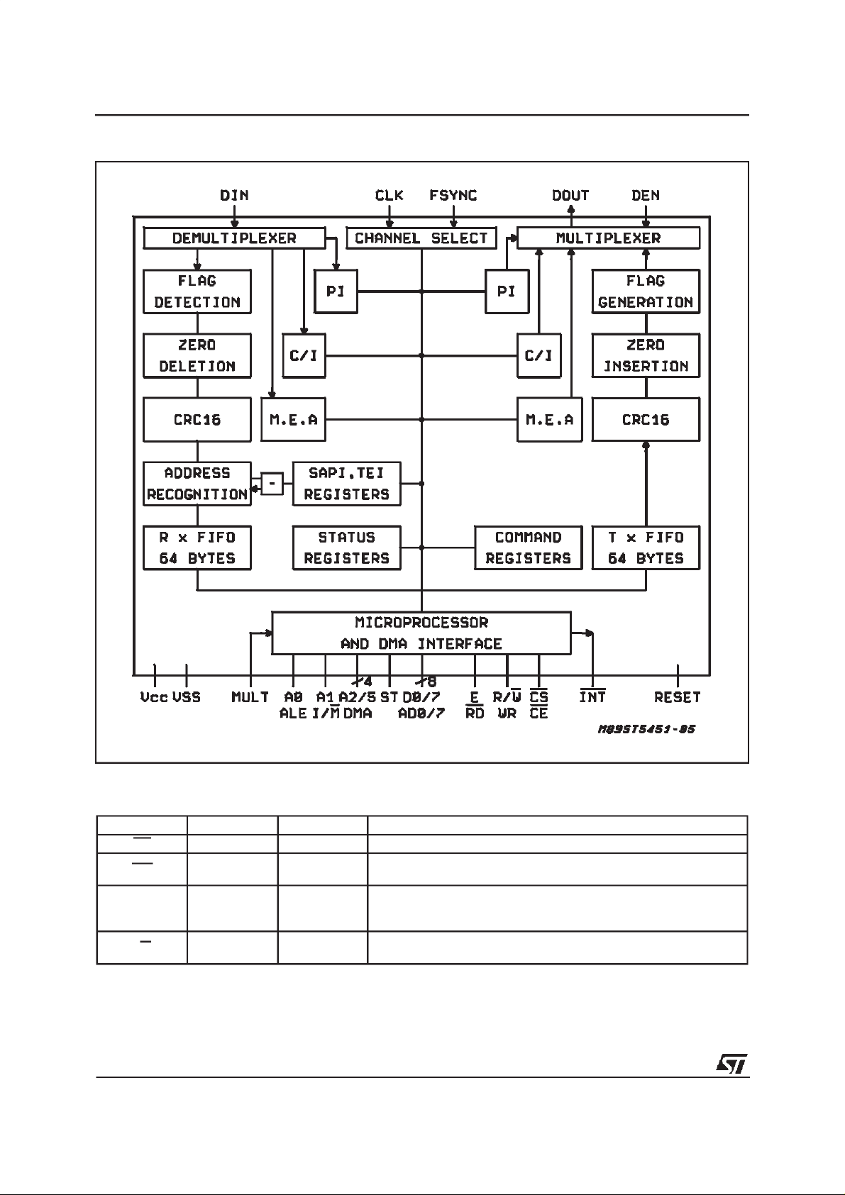
BLOCK DIAGRAM
PIN DESCRIPTION
NAME PIN TYPE FUNCTION
CS 1 I Chip Select. A lowlevel enables ST5451 forread/write operations.
INT 25 O
MULT 2 I
I/M 4 I
2/34
Interrupt request is asserted by ST5451 when it request aservice.
Open drain output.
Multiplexed Bus. Indicates the
MULT = 1: multiplexed bus andDMA available.
MULT = 0: address and data bus separated.
Intel/Motorola. When MULT = 1 this pin selects either Intel or
Motorola 6805 bus.
P bus interface selected.
µ

DEMULTIPLEXED MICROPROCESSOR BUS INTERFACE (MULT = 0)
NAME PIN TYPE FUNCTION
A0/A5 3-8 I Address Bus. To transfer addresses from
D0/D7 17-24 I/O Data Bus. To transfer data between
R/W 27 I Read/Write. ”1” indicates a read operation; ”0” a write operation.
E26I
Enable. Read/write operations are synchronized with thissignal; its
falling edge marks the end of an operation.
µP to ST5451.
P and ST5451.
µ
MULTIPLEXEDMICROPROCESSORBUS INTERFACE (MULT = 1 I/M=1)
NAME PIN TYPE FUNCTION
AD0/AD7 17-24 I/O
WR 27 I Write. This signal indicates a write operation.
RD 26 I Read. This signal indicates a read operation.
ALE 3 I Falling edge latches the address from the external A/D Bus.
Address Data Bus. To transfer addresses and data between
and ST5451.
MULTIPLEXEDMICROPROCESSORBUS INTERFACE (MULT = 1;I/M=0)
NAME PIN TYPE FUNCTION
AD0/AD7 17-24 I/O
R/W 27 I Read/Write. ”1” Indicates a write operation; ”0” a write operation.
DS 26 I
AS 3 I
Address Data Bus. To transfer addresses and data between
and ST5451.
Data Strobe. Read/Write operations are synchronized with this
signal: its falling edge marks the end ofan operation.
Address Strobe. Fallingedge latches the address from the external
A/D Bus.
ST5451
µP
P
µ
DMA (directmemory access): only when MULT = 1
NAME PIN TYPE FUNCTION
DMA REQ X
DMA REQ R
DMA ACK X
DMA ACK R
7
5
8
6
O
O
I
I
Direct Memory Access Requests: these outputs are asserted by
the device to request an exchange of byte from the memory.
Direct Memory Access Acknowledge: these inputs are asserted by
the DMA controller to signal to the HDLC controller that a byte is
being transferred in response to a previous transferrequest.
GCI INTERFACE
NAME PIN TYPE FUNCTION
D
OUT
D
IN
C
LK
FS 13 I
DEN 10 I
15 I/O
12 I/O
11 I
Data output for Band D channels. In GCI mode it outputs B1,
B2, M and C/I channels. InTE mode (GCI-SCIT) it can invert to
input data for M’ and C/I’ channels (See Table 2).
Data input for B and D channels. In GCI mode it inputs B1, B2, M
and C/I channels. In TE mode (GCI-SCIT) itcan invert tooutput
data for M’ and C/I’ channels (See Table 2).
Data Clock. It determines the data shift rate for GCI channels on
the module interface.
Frame synchronization. This signal is a 8 kHz signal for frame
synchronization. The front edge gives the time reference of the first
bit in theframe.
Data Enable. In TE mode, this pin is a normally low input pulsing
high to indicate the active bit times for D channel transmit at DOUT
pin. It is intended to be gated with CLK to control the shifting of
data from HDLC controller to S interface device.
3/34
ST5451
NON GCI INTERFACE
NAME PIN TYPE FUNCTION
Data output. Digital output for serial data. Three modes:
D
OUT
D
IN
C
LK
FS 13 I
DEN 10 I Data Enable. When high, enable the data transfer. on D
15 O
12 I Data input. Digital input for serial data. Three modes (See D
11 I
OTHERS
NAME PIN TYPE FUNCTION
V
DD
V
SS
R
ST
ST 9 I Special Test. (Reserved) must be tied to V
28 I Positive power supply = 5V +5%
14 I Signal ground
16 I Reset
- HDLC Protocol multiplexed link
- HDLC Protocol non multiplexed link
- Non HDLC protocol (transparent Mode).
Data Clock. It determines the data shift rate. Two modes: Single or
double bit rate.
Frame synchronization. Used in mode HDCL protocol multiplexed
link. Don’t care in other modes. The rising edge gives the time
reference of the first bit of the frame.
SS
OUT
OUT
).
2 - FUNCTIONS
2 - 1 - Basic HDLC Functions
2 - 1 - 1 - In Receive Direction:
- Channel selection
In GCI channel B1 or B2 or D may be selected.
B1 or B2 may be selected without M and C/I
channels
- Flag detection
A zero followedby six consecutiveones and another zero is recognizedas a flag
- Zerodelete
A zero, after five consecutive ones within an
HDLC frame, is deleted
- CRC checking
The CRC field is checked according to the generator polynomial
16+X12+X5
X
+1
- Check for abort
Seven or more consecutiveones are interpreted
as an abort flag
- Check for idle
Fifteen or more consecutive ones are interpretedas ”idle”
- Minimumlenght checking
HDLC frames with less than n bytes between
start and end flag are ignored: allowed values are3 ≤
n ≤ 6.
This value is set by aprogrammable register
- Address Field recognition
4 SAPI and/or 3 TEI may be recognized. Several programmableregisters indicate the recognized address types.
2 - 1 - 2 - In TransmitDirection:
- Shift control in TE mode
D channeldata are signalled by DEN pin.
- Flag generation
A flag is generated at the beginning and at the
end of every frame.
- Zero insert
A zero is inserted after five consecutive ones
within an HDLC frame
- CRC generation
The CRC field of the transmittedframe is generated according to the generatorpolynomial
16+X12+X5
X
+1
- Abort sequencegeneration
An HDLC frame may be terminated with an
abort sequence under microprocessorcontrol
- Interframetime fill
Flags or idle (consecutive ones) may be transmitted during the interframe time. A programmable bitselects the mode.
4/34

ST5451
2 - 2 - FIFO Structure
2 - 2 - 1 - Receive FIFO Structure
In receive direction, a 64 byte FIFO memory is
used. It is divided in 8 blocks of 8 bytes automatically chained.
In case of a frame length of 64 bytes or less,the
whole frame can be stored in the FIFO. After the
first 32 bytes have been received µP is interrupted and may read the availabledata.
In case of frames longer than 64 bytes, the µPis
interruptedto read out the FIFO by 32 byte block.
In caseof several shortframes, up to eight may be
storedinside the FIFO.Afteran interrupt, one frame
is available for the µP. The eventual other seven
framesare queuedand transferredoneby one.
2 - 2 - 2 - TransmitFIFO Structure
In transmit direction, a 64 byte FIFO memory is
TABLE 1
- ST5451 Internal Registers
Address Hexa Read Write
00 Receive FIFO Transmit FIFO
1F - 20 ISTA0 ISTA0
21 ISTA1 ISTA1
22 ISTA2 ISTA2
23 STAR CMDR
24 MODE MODE
25 RFBC TSR
26 CA CA
27 CB CB
28 CC CC
29 CD CD
2A CE CE
2B CF CF
2C CIR1 CIX1
2D CIR2 CIX2
2E MONR1 MONX1/0
2F - MONX1/1
30 MONR2 MONX2/0
31 - MONX2/1
32 - MASK0
33 - MASK1
34 - MASK2
3E CCR CCR
used, structured in 2 blocksof 32 bytes. ST5451
is requested to transmit after 32 bytes have been
written into the FIFO.
If a transmission request does not include a message end, the HDLC controller will request the
next data blockby an interrupt.
2 - 3 - MicroprocessorInterface
Three types of microprocessor interfaces are
available (MULT and I/M control pins set the desired interface).
- Motorola non multiplexedfamilies.
- Motorola multiplexed family (6805 type)
- Intel family.
You can connect ST5451 to a Direct Memory Ac-
cessController as MC68440 or MC6450 (dual or
quad channels).
A programmable register indicates DMA Interface
enabling.
5/34
ST5451
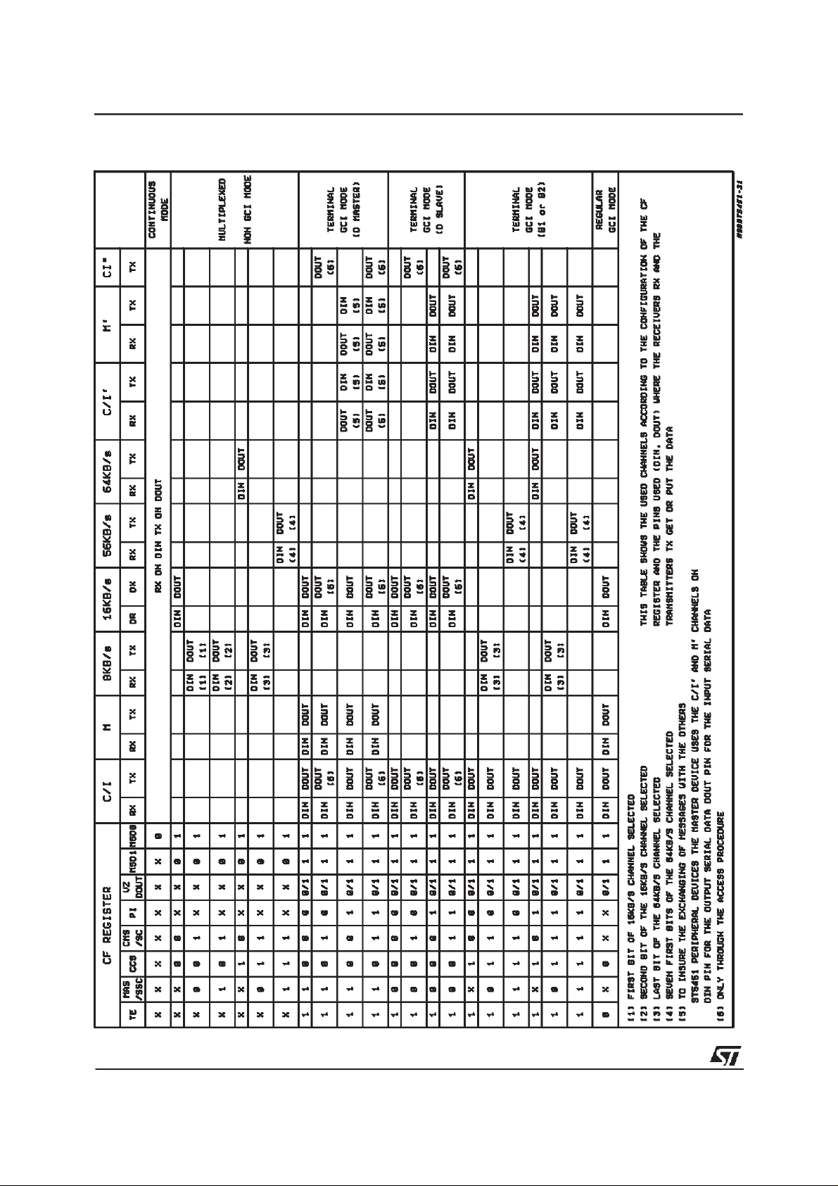
TABLE 2 - CHANNEL ASSIGNMENTSELECT
6/34

ST5451
3 - REGISTERDESCRIPTION
For all the register pictures MSB is on the left and
LSB on the right
Ifnototherwisestatedbitareconsideredactiveat1.
FIFOS
RFIFO (read), XFIFO (write).
The address range of the two FIFOs are identical.
All the 32 addresses give access to the ”current”
FIFO location.
When the closing Flag of a receive frame is detected, a status byte is available in the RFIFO.
This byte has the following format:
RBC RDO CRC RAB 0 0 0 0
RBC ReceiveByte Count.
The length of the received frame is n
time 8 bits (n=3,4,5,...)
RDO Receive Data Overflow
A part of the frame has not been lost
becausethe receiveFIFO was full
CRC CRC Check
ThereceivedCRCbyteswerenotcorrect
RAB Receive Abort
The received framewas not aborted
A status byte equal to D0H indicates a correctly
received frame
enteredinto the XFIFO.
XDU TransmitData Underrun
A transmitted frame was terminated
with an abort sequence because no
data were available for transmission in
XFIFO and no XME command was issued. It is not possible to transmit
frame when that interrupt remains unacknowledgedand XRES has not been
set.
EXI2 Extended Interrupt2
The interruptreason is indicated in register ISTA2
EXI1 ExtentedInterrupt1
The interruptreason is indicated in register ISTA1.
ISTA1 InterruptStatus Register 1
After RESET 01H
(GCI mode only)
0 0 CIC1 EOM1 XAB1 RMR1 RAB1 XMR1
CIC1 Comman/IndicateChange
A change in the value of CIR1 is detected
EOM1 End of Message1 (monitorchannel)
MON1 has received an end of message.
XAB1 MonitorTransmit ABORT
The received byte has not been detectedin two successiveframes.
MON1 has sent an ABORT (A bit) to
the remote transmitter.
ISTA0
InterruptStatus Register 0
AfterRESET 10H
RME RPF RFO XPR XDU EXI2 EXI1 0
RME
ReceiveMessage End
One complete frame of length less than
or equal to 32 bytes, or the last part of
a frame of length greater than 32 bytes
is stored in the RFIFO.
RPF ReceivePool Full
32 bytes of a frame are in RFIFO. The
frame is not yet completelyreceived.
RFO ReceiveFrame Overflow
A complete frame was lost because no
storage space was available in the
RFIFO.
XPR Transmit Pool Ready
One data block (32 bytes max) may be
RMR1 ReceiveMonitor Register1 ready
A byte has been received in register
MONR1.
RAB1 ReceiveAbort
MON1 received an ABORT from the remote receiver.
XMR1 Transmit Monitor Register 1 ready
A byte can be stored in register
MONX1
ISTA2
InterruptStatus Register 2
After RESET 01H
(GCI and TE modeonly)
0 0 CIC2 EOM2 XAB2 RMR2 RAB2 XMR2
CIC2 Command/IndicateChange
A change in the value of CIR2 is detected.
7/34

ST5451
EOM2 End of Message2 (monitor channel)
MON2 has received an end of message.
XAB2 Monitor Transmit ABORT
The received byte has not been detectedin two successive frames.
MON2 has sent an ABORT (A bit) to
the remote transmitter.
RMR2 Receive Monitor Register2 ready
A byte has been received in register
MONR2.
RAB2 ReceiveABORT
MON2 received an ABORT from the remotereceiver.
XMR2 TransmitMonitor Register 2 ready
A byte can be stored in register
MONX2.
MASK0, MASK1, MASK2
After Reset FF; the three mask registers MASK0,
MASK1, MASK2 are associated respectively to
the three interrupt registers ISTA0, ISTA1,and
ISTA2.
Each interrupt source in ISTA registerscan be selectively masked by setting to ”1” the corresponding bit in MASK1. Interrupt sources (masked or
not) are indicated when ISTA is read by the microprocessor. When an interrupt source is not
masked, INT goes low.
STAR Status Register
AfterReset 48H
XDOV XFW IDLE RLA DCIO 0 0 0
XDOV TransmitData Overflow
More than 32 bytes have been written
into the XFIFO.
XFW XFIFOWrite enable
Data can be entered into the XFIFO.
IDLE IDLE State
15 or more consecutive ones have
been detectedon the input data line.
RLA Receive Line Active
Frames or interframe flags are being
received
DCIO D and C/I Channels are occupied
CMDR CommandRegister
After Reset 00
XHF XME RMC RMD RHR XRES M2RES M1RES
XHF HDLCframe transmission can start.
XME Transmit MessageEnd
The last part of the frame was entered
in XFIFOand can be sent.
RMC Receive Message Complete
Reaction to RPF or RME interrupt. The
received frame (or one pool of data)
has been read and the corresponding
RFIFOis free.
RMD Receive Message Delete
Reaction to RPF or RME interrupt. The
entire frame will be ignored. The part of
frame already stored is deleted.
RHR Reset HDLC receiver
XRES Reset HDLC transmitter
XFIFO is cleared and the transmitted
frame (if any) is aborted.
M2RES Monitor2 Reset
Reset MONITOR and C/I channels (TX
and RX).
M1RES Monitor1 Reset
Reset MONITOR and C/I channels (TX
and RX).
* For the four first bits (XHF, XME, RMC,
RMD), the reset is done by the device;
the other bits level sensitive
MODE HDLC Mode Register
After Reset 00
DMA FL1 FL0 ITF RAC CAC NHF FLA
DMA DMA Interfaceactivation
FL1/0 Frame Length
Minimum framelength accepted
FL1 FL0
3 bytes
4 bytes
5 bytes
6 bytes
0
0
1
1
0
1
0
1
ITF InterframeTimeFill
ITF= 1 : Flags are transmitted
ITF= 0 : IDLE is transmitted
8/34
RAC RAC=1 : ActivateRX
RAC= 0 : deactivateRX

ST5451
CAC ChannelActivation
CAC= 1 : Activate RX and TX
CAC= 0 : deactivate RX and TX
NHF HDLC Function Select
NHF = 1 :disable HDLC function
FLA Flag
FLA = 1 : transmitshared flags
FLA = 0 : transmittwo flags between
consecutiveframes.
RFBC ReceiveFrame Byte Counter
Afterreset 00
RDC7 RDC6 RDC5 RDC4 RDC3 RDC2 RDC1 RDC0
RDC 0/7 ReceiveData Count
Total number of bytes of received
frame without CRC.
RDC 0/4 Indicate the number of bytesin the cur-
rent block available in RFIFO.
RDC 5/7 Indicate the number of 32 bytes blocks
received. If the frame exceeds 223
bytes, RDC 5/7 hold the value ”111”,
only RDC 4/0 continueto count modulo
32.
See Table3.
The contents of the register are valid after an
RME interrupt. The µP must read N+1 bytes to
transfer the number of bytes received and the
status byte into the memory.
MONX1 Monitor Transmit Register 1
After reset FFH
(GCI only)
M1 M2 M3 M4 M5 M6 M7 M8
The value written in MONX1 is transmitted in the outgoing Monitor channel
according to GCI transfer protocol.
XMR1 interrupt indicates when MONX1
is again available.
MONR1
MonitorReceive Register 1
After reset FFH
(GCI only)
M1 M2 M3 M4 M5 M6 M7 M8
The value read from MONR1 gives the
value of the byte received in the monitor channel according to GCI transfer
protocol. RMR1 interrupt indicates
when a new byte is available in
MONR1register.
CIX2 Command/IndicateTransmitRegister 2
After Reset FFH
(GCI and TE modeonly)
1 1 P1 P2 P3 P4 P5 P6
P1/P6 Code transmitted permanently in the
2nd GCI C/I channel.
CIX1 Command/IndicateTransmitRegister1
Afterreset FFH
(GCIonly)
1 1 1 1 C1C2C3C4
C1, C2, C3, C4:
Code to be transmitted permanently
in the outgoing GCI C/I channel.
CIR1
Command/IndicateReceiveRegister 1
Afterreset FFH
(GCIonly)
1 1 1 1 C1C2C3C4
C1, C2, C3, C4:
Incoming GCI C/I channel.
CIR2 Command/IndicateReceive Register 2
After reset FFH
(GCI and TE modeselected only)
1 1 P1 P2 P3 P4 P5 P6
P1/P6 The contents of the 2nd C/I channel;
they are the different requests received
from TE peripheral devicesto µP.
Six peripherals can make a simultaneous request.
MONX2
MonitorTransmit Register 2
After reset FFH
(GCI and TE modeonly)
The value written in MONX2 is transmitted in the 2nd GCI M channel to a
peripheral(if PI= 1; registerCF).
9/34

ST5451
TABLE 3
N (number of bytes in the
frame received without CRC)
Nnmn
1 Min 000 00001 0
2 000 00010 0
3 000 00011 0
30 000 11110 0
31 000 11111 0
32 001 00000 1
33 001 00001 1
62 001 11110 1
63 001 11111 1
64 010 00000 2
222 110 11110 6
223 110 11111 6
224 111 11111 7
256 111 00000 7
257 111 00001 7
- 111 - 7
Counter n (number of 32 bytes blocks
765 43210
received )
MONR2
Monitor ReceiveRegister 2
Afterreset FFH
(GCIand TE mode only)
The value read from MONR2 gives the
value of the byte received from M
channel in 2nd GCI channel.
TSR Time Slot Register
Afterreset 00
TSR7 TSR6 TSR5 TSR4 TSR3 TSR2 TSR1 TSR0
In GCI mode (MDS1= 1 in CF Register)
a) CCS=1in CFReg. (64 Kbit/s)
Then: TSR2 indicatesB1 or B2
TSR4/7indicate positionof
GCI channel
b) CCS=0in CF Reg. (16 Kbit/s)
Then: TSR4/7indicate positionof
GCI and its D channel
In Multiplexed Mode
(MDS1=0in CF Register)
a) CCS=1 in CF Reg. (64 Kbit/s)
Then: TSR2/7 indicatechannel
positionin the 64 timeslots
multiplex
b) CCS=0 in CF Reg. (16 Kbit/s)
Then: TSR0/7 indicatechannel
positionin the 256 timeslots
multiplex.
CA ConfigurationnRegister A
After reset 00
CA7 CA6 CA5 CA4 CA3 CA2 CA1 CA0
CA0 SAPI 0 is recognized CA0 = 1
CA1 SAPI 63 CA1 = 1
CA2 SAPI x CA2 = 1
CA3 SAPI y CA3 = 1
CA4 TEI 127 CA4 = 1
CA5 TEI z CA5 = 1
CA6 TEI t CA6 = 1
CA7 Address filter active CA7 = 1
CB ConfigurationregisterB
After reset 00
Contentof CBindicate SAPI x value
HighOrder 6 Bits
SAPI 0 0
CC ConfigurationRegister C
After reset 00
Contentof CCindicate SAPI y value
HighOrder 6 Bits
SAPI 0 0
10/34
ST5451
CD ConfigurationRegister D
Afterreset 00
Contentof CD indicateTEI z value.
7 High Order Bits
TEI 0
CE ConfigurationRegisterE
Afterreset 00
Contentof CE indicateTEI t value.
7 High Order Bits
TEI 0
CF Configuration RegisterF
After00
TE MAS/SSC CCS CMS/SC PI VZDOUT MDS1 MDS0
TE TE mode
TE = 1 : the frame is constitued by
three GCI channels (GCI-SCIT)
MAS/SSCIf CCS= 0, TE = 1, MDS0and MDS1= 1
(i.e. GCI mode, TE mode, 16 Kbit/s)
MAS/SScis MAS and:
MAS = 0 means ”Slave device”
MAS = 1 means ”Master device”
If SC = 1 (i.e. a sub-channel is selected)MAS/SSC is SSC; if 16Kb is selected SSC chooses between first on
second bit of the stream while, if 64Kb
is selected SSC chooses between first
or last seven bits of the stream (see
TABLE 2 and CMS/SC)
CCS ChannelCapacity Selection
CCS= 1: 64 Kb/s
CCS= 0: 16 Kb/s.
CMS/SC If CCS= 0, TE= 1,MDS0andMDS1= 1
(i.e. GCI mode, TE mode, 16Kbit/s)
CMS/SC is CMS (Contention mode selection)and:
CMS = 1 means ”D and C/I channel
accessprocedure active”
CMS = 0 means ”D and C/Z channel
accessprocedure active”
If CCS = 1 and TE = 1 CMS/SC is SC
(Subchannel)and:
SC = 0 means ”16Kbit/sor 64Kbit/sis
used”
SC = 1 means ”an 8Kbit/s or 56Kbit/s
subchannelinside a 16Kbit/sor
64kbit/sisused”(seeMAS/SSC)
PI PeripheralInterface (only if TE=1)
PI = 1: CIX2, CIR2, MONX2, MONR2,
active
VZDOUT When level 1 device is inactive (i.e.
CIR1 = DI = 1111) and GCI has to be
wakenup (i.e. TIM = 0000 in CIX1),
DOUT is set to zero requiring FS
and CLK if VZ DOUT=1.
MDS1 Mode Bit 1
MDS1 = 1:GCImode
MDS1 = 0: Multiplexed mode
MDS0 Mode Bit 0
MDS0 = 1: Multiplexer and Demultiplexer are active.
MDS=0No multiplexer.
CCR ConfigurationRegister 00
After reset 00
TLP ADDR AD3 AD2 AD1 AD0 CRS TRI
TLP Test Loop
TLP = 1: The transmitter is internally
connected to the receiver; the transmit
output is not activated.The digital interface must be activated to provide the
bit clock and frame Synchro.
ADDR Address Recognized
If TE= 1 and PI = 1
ADDR = 1: The first byte received in
MONR2 is compared with AD0/3. If
equal the message is accepted, otherwise is ignored.
ADDR = 0: The message is always accepted.
AD0/3 When PI = 1, is the component ad-
dress.
AD0/2 Address bit used to access D and C/I
channels (TE = CMS =1, CCS = 0).
CRS ClockRate Selection
CRS = 1: Clock frequency is twice the
data rate (GCI).
CRS = 0: Clock frequency and data
rate are identical.
TRI Tristate
TRI = 1: DOUT in tristate
TRI = 0: DOUT in open drain.
11/34
 Loading...