

ST52T301/E301
8-Bit OTP/EPROM DuaLogic
MCUs WITHADC,
UART,TIMER, TRIAC & PWM DRIVER
ADVANCED DATA SHEET
HighSpeeddedicatedstructuresforFuzzyLogic
(3.5µs to computea4 Inx 1 Outrule)
Cap ability to pe rfor m simple boolean and
arithmetic operations
Up to4Input,2OutputConfigurableVariablesfor
each Fuzzy Algorithm and up to 300 Rules
Up to16 Triangularand TrapezoidalMembership
Functionsfor each Input variable
Up to 256 Singleton Membership Functions for
all Consequents
Programand DataEPROM:2 Kbytes
16 ge neral purpose registers available as
RegisterFile
Working ClockFrequencies:5, 10and 20MHz
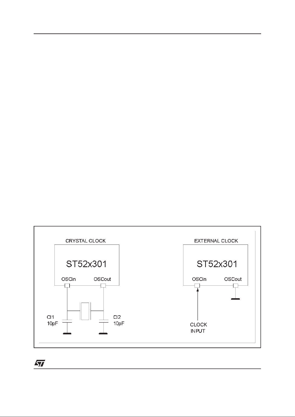
On-Chip Clock Oscillator driven by Quartz
Crystal or CeramicResonator
One externalinterrupt
StandardTTL compatibleinput
CMOScompatibleoutput
4 channel8 bitAnalogto DigitalConverter
Bandgapreference2.5V
Digital 8 bitI/O port indepedentlyprogrammable
with handshakesignal
Serial Communic ation Interface with
asynchronousprotocol (UART)
ProgrammableTimer with internalPrescaler
Internal Power Fuzzy Control to drive external
Triac (up to 25mA source,50 mA sink current)
Internal Fuzzy controlled PWM to drive an
external powerdevice
Softwaretools and Emulatorsavailability
Windowed and One Time Programmable(OTP)
Memory parts available for prototyping and
production phases
44 pinPlastic(PLCC44)andCeramicWindowed
LeadedChip Carrier (CLCC44-W)
July 1998
CLCC44-W
PLCC44
1.1 GENERAL DESCRIPTION
ST52E301
(1)
and ST52T301
(1)
devices are
membersof the W.A.R.P.familyof 8-bit
DuaLogic
microcontrollers. They are able to perform, in an
efficientway,both booleanand fuzzyalgorithms,in
order to reach thebest performancesthat the two
methodologiesallow.
TheST52E301istheerasableEPROMversionand
the ST52T301 is the OTPversion.
The ST52x301 is completely developed and
producedby STMicroelectronicsusing the reliable
high performanceCMOSM5E(O.7µm) process.
Thanks to Fuzzy Logic, ST52x301 allows to
describea problemusing alinguisticmodelinstead
ofa mathematicalmodel.Inthiswayitisveryuseful
and easy to modelize complex system with very
high accuracy.
The linguistic approach is based on a set of
IF-THEN rules, describing the control behaviour,
and on MembershipFunctions associatedto input
and output variables.
Fuzzy Inference is a set of operations which
computes the output values according with the
truthvalues of the involvedrules.
Note: (1) Formerly W.A.R.P.3TC
1/99
The flexible I/O configurationof ST52x301 allows
to interface with a wide rangeof external devices,
likeD/A converters, powercontroldevices(SCRs,
TRIACs) and externalsensors.
TheOTP (OneTimeProgrammable)deviceis fully
compatible with the EPROM windowed version,
which may be used to create prototype systems
and for the pre-productionphases.
The Fuzzy Core includes the fuzzifier (ALPHA
calculator),the inferenceunit and thedefuzzifier.
It allowsto manage up to 300Rules(4 Inputs and
1 Output).The rules could be shared in different
fuzzy subroutines that can be activated by user
defined conditions.
The I/O capabilities, demanded from
micro con troller applications, a re f ulfilled by
ST52x301with 4 AnalogInputs, an asynchronous
Peripheral interface (UART) and an 8-bit I/O
communicationport inorderto transferdatafrom/to
the on-chip RegisterFile.
The voltage reference provides biasing to the
analogportion ofthe internal circuitry. Theinternal
referenceis a 2.5V Bandgapreference.
The voltage referencecan supply up to0.1 mA of
currentto power externalcircuitry.
ST52x301 includesan 8-bitsampling Analogto
Digital (A/D) Converter with a 4 analog
channel fast multiplexer (32µs conversion
time/channel ).
It is possibleto perform operationson data stored
in the RegisterFile (16bytes),allowing to manage
newinputs and feedbackoutputs.
The TRIAC/PWM Driver peripheral allows to
manage directly power devices, implementing
three different operating modes: Burst Mode
(i.e.Thermal Applications), Phase Angle
Partialization (i.e.Motors Control by TRIACs) and
high frequency PWM controls.
A programmable Timer with Internal Prescaler,
using both internal or externalclock, is available.
The microcontroller configuration is stored in the
internalEPROM.
A powerful development environment,
FUZZYSTUDIO 3.0, consisting of a boa rd
and software tools, allows an easy
configuration and use of ST52x301.
ST52x3 01 is f ully sup por ted by
FUZZYSTUDIO3.0 software tools allowing
to graphically design a projectand obtainan
optimizedmicrocode.
ST52x301 exploits a SGS-THOMSON patented
strategyto store the MFs in its internal memory.
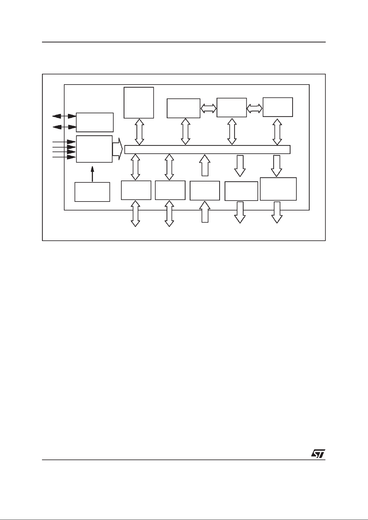
OSCILLATO R
ALU
-
FUZZY
CORE
SYSTEM
REGISTERS
CONTROL
UNIT
REGISTER
FILE
PARALLEL
I/O PORT
2kBytes
EPROM
TRIAC/PWM
DRIVER
PROG.TIMER
WITH
PRESCALER
SCI
A/D
CONVERTER
BAND-GAP
REFERENCE
Figure1.ST52x301ArchitecturalBlock Diagram
2/99
ST52T301/E301
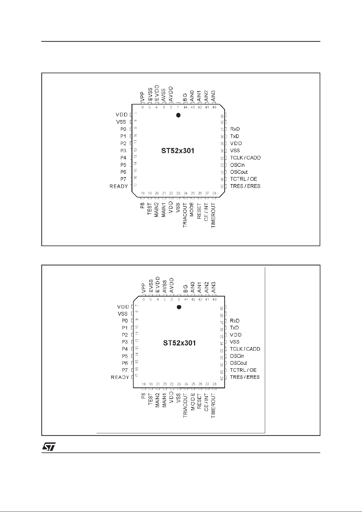
Figure 2.CLCC44-W Pin Configuration
Figure3.PLCC44 Pin Configuration
3/99
ST52T301/E301

PIN NAME TYPE Programming Phase Working Phase
1 not connected - -
2 AV
DD
Analog V
DD
Analog V
DD
3 AV
SS
Analog Ground Analog Ground
4 EV
DD
EPROM Digital Power Supply EPROM Digital PowerSupply
5 EV
SS
EPROM Digital Ground EPROM DigitalGround
6 V
PP
EPROM Programming
Powersupply (12V
±5%)
EPROMV
DD
(5V ±10%)
7 V
DD
Digital Power Supply Digital Power Supply
8 V
SS
Digital Ground Digital Ground
9 P0 I/O I/O EPROM Data Digital I/O
10 P1 I/O I/O EPROM Data Digital I/O
11 P2 I/O I/O EPROM Data Digital I/O
12 P3 I/O I/O EPROM Data Digital I/O
13 P4 I/O I/O EPROM Data Digital I/O
14 P5 I/O I/O EPROM Data Digital I/O
15 P6 I/O I/O EPROM Data Digital I/O
16 P7 I/O I/O EPROM Data Digital I/O
17 READY O I/O port Handshaking Signal
18 P8 O Digital Output
19 TEST I (must be set to 0) (must beset to 0)
20 MAIN2 I/O Zero Crossing/Prescaler Output
21 MAIN1 I Zero Crossing
22 V
DD
Digital Power Supply Digital Power Supply
23 V
SS
Digital Ground Digital Ground
24 TRIACOUT O Triac/PWM DriverOutput Pulses
25 MODE I Functionment Mode Selector Functionment Mode Selector
26 RESET I General Reset General Reset
27 CE/INT I Chip Enable EPROM External Interrupt
28 TIMEROUT O Output Timer
29 ERES / TRES I EPROM Address Counter Reset External TimerReset
30 OE / TCTRL I EPROM OutputEnable Timer Start/Stop Signal
31 OSCout I/O Oscillator Output Oscillator Output
32 OSCin I Oscillator Input Oscillator Input
33 CADD /TCLK I EPROM Change Address Clock Timer External Clock
34 V
SS
Digital Ground Digital Ground
35 V
DD
Digital Power Supply Digital Power Supply
36 TxD O SCI Output
37 RxD I SCI Input
38 not connected - -
39 not connected - -
40 AIN3 Ainp Analog Input
41 AIN2 Ainp Analog Input
42 AIN1 Ainp Analog Input
43 AIN0 Ainp Analog Input
44 BG Aout Band Gap Output
Table1.PLCC44 and CLCC44-WPin Configuration
4/99
ST52T301/E301

1.2 PIN DESCRIPTION
V
DD,EVDD,VSS
,
EV
SS,AVDD
,AV
SS,VPP
.
In order to
avoidnoise disturbances,the power supplyof the
digitalpartis keptseparatedfromthepowersupply
of the analogpart.
V
DD.
MainPowerSupply Voltage(5V 10%).
V
SS
.Digitalcircuit Ground.
EV
DD.
EPROM Main Power Supply Voltage (5V
10%).
EV
SS
.EPROMDigitalcircuit Ground.
AV
DD
. Anal og VDDof the Analog to Digital
Converter.
AV
SS
.AnalogVSSoftheAnalogtoDigitalConverter.
Must be tiedto VSS.
VPP. Main Power Supply for the internal EPROM
(12.5V5%).
OSCin and OSCout. These pins are internally
connected with the on-chip oscillator circuit. A
quartz crystal or a ceramic resonator can be
connectedbetweenthesetwopinsinordertoallow
the correct operations of ST52x301 with various
stability/cost trade-offs. An external clock signal
canbe appliedtoOSCin,in thiscaseOSCoutmust
be grounded.
RESET
.Thissignalis used torestart ST52x301at
thebeginningof itsprogram.Italsoallowsto select
the program mode forthe EPROM.
INT
. External interrupt active on rising or falling
edge.
AIN0-AIN3. These 4 lines are connected to the
inputs of the analog multiplexer. They allow to
acquire4 analoginputs.
BG
.A Voltageequalto 2.5Visavailableonthispin.
It can be used forAnalogsignal conditioning.
P0-P7.These8 lines areorganizedas oneI/Oport.
During the Programmingphase such port is used
forthe EPROM data read/write.
READY.Handshakesignal of the parallelport.
P8.Digital output.
TxD. Serial data output of the SCI transmitter
block.
RxD
. Serial data input of the SCI receiver
block.
TRES,TCLK,TCTRL, TIMEROUT.These pins are
relatedwith the internalProgrammableTimer.The
Timer can be reset externally by using TRES. In
Working Mode, TRES resets the address counter
of the Timer.TRES is active atlowlevel
The Timer Clock can be the internal clock or can
be supplied externally by using the pin TCLK.
AnexternalStart/Stopsignalcanbeusedto control
theTimerthroughthepinTCTRL.TheTimeroutput
is availableon thepin TIMEROUT.
MAIN1,MAIN2,TRIACOUT
. ST52x301 is able to
drive a TRIAC in two different modes:Burst mode
or Phase AnglePartializationcontrolmode.
The Burst mode is usedforthermal regulation.
MAIN1 and MAIN2 signals are used to detect the
zero crossingof the main voltage.
ThepulsetodrivetheTRIACis givenbyTRIACOUT
pin.
It is possible to use the samepins to implement a
PWM Driver. In this case it is possible to fix the
periodof PWMand to changethe dutycycleon fly.
ThePWM output isgiven by TRIACOUT pin.
CE,OE,ERES,CADD,V
PP
. These pins are used
to manage the EPROM during the Programming
phase. During the Programming phase
(programming) V
PP
must be set at 12V. In the
Working phase V
PP
mustbe equalto VDD.
ERES in Programming Mode resets the address
counterof the EPROM;it is active athigh level.
Inthe Workingphase OE,CE andCADDare used
likehandshakingsignalsfor the parallelport.
MODE
. It selects the function ment mo de
(Programmingor Working mode).
TEST.It enablesthe testing functionalities;during
theProgrammingandWorkingphaseitmustbeset
to 0.
5/99
ST52T301/E301
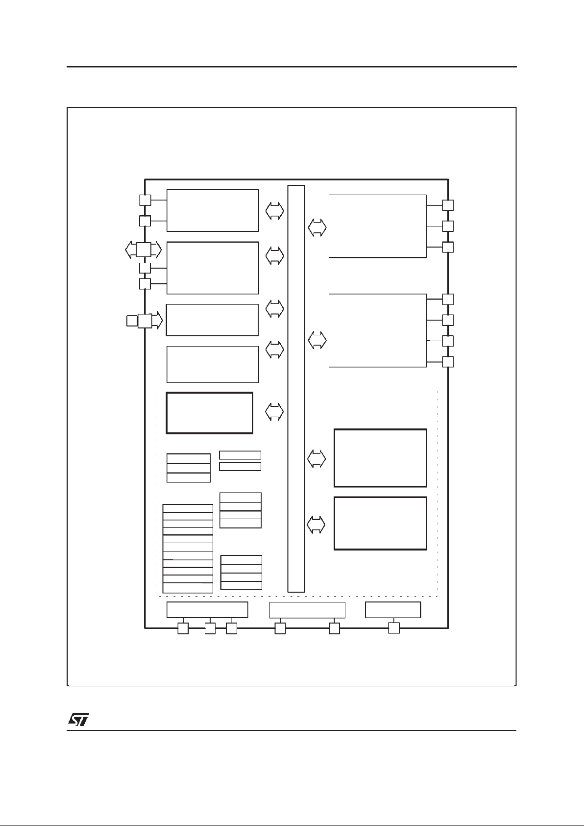
2 INTERNAL ARCHITECTURE
ST52x301is made up by the followingblocksand
peripherals:
Control Unit
Fuzzy Core
ALU
EPROM
Clock Oscillator
Analog Multiplexerand A/D Converter
PrescalerTimer
Bandgap
Triac/ PWMDriver
Digital I/O port
Serial Communication Interface
ST52x301Operating Modes
ST52x301works in twomodes,Programmingand
Working Modes,dependingon the controlsignals
levelRESET, TESTand MODE.
The Operatingmodes are selected by setting the
control signal level as specified in the Control
SignalsSettingtable.
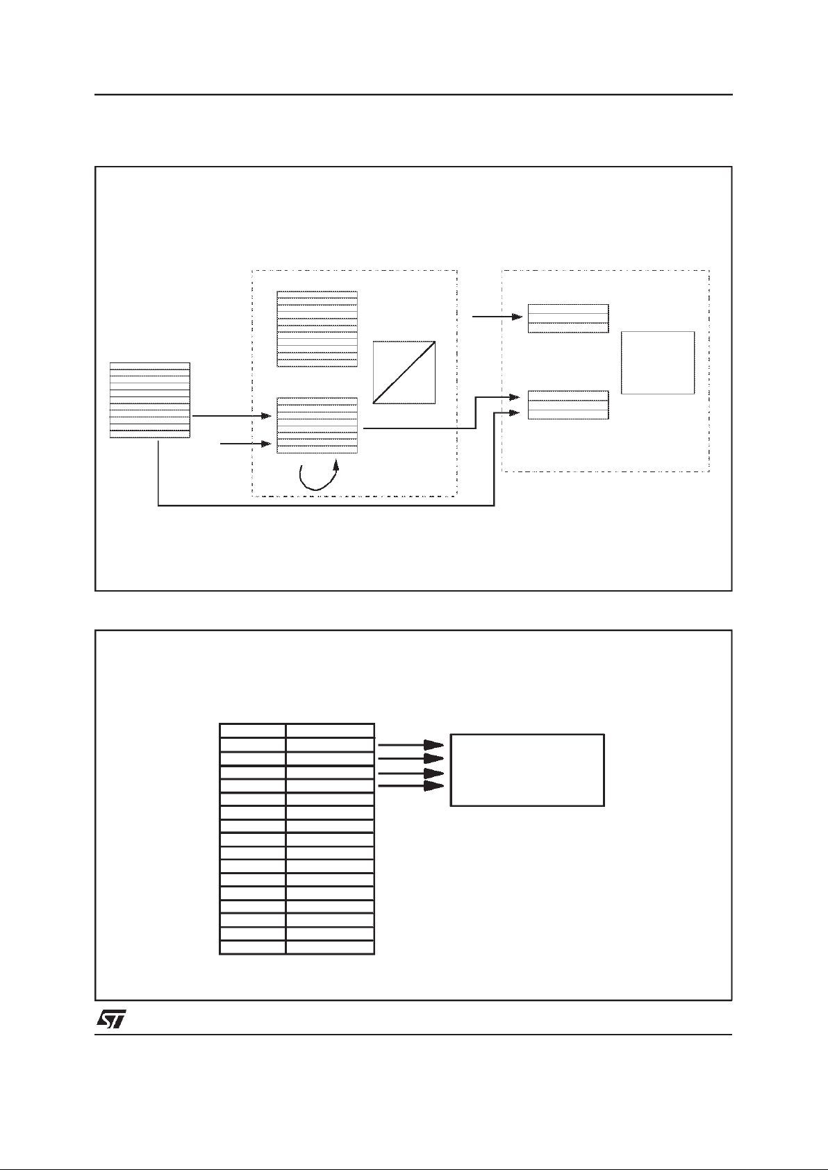
2.1 CONTROL UNIT
The Control Unit (CU) manages: Registers File,
Input Registers, Configuration Registers, ALU,
Accumulatorand Multiplexerinputs.Moreoverthe
CU drives the Fuzzy Core and the peripherals
(Triac/PWM Driver andTimer).
The CU reads the stored instructions on the
EPROM (Fetch) and decodifies them. If the
instructions are arithmetic or logic, the CU runs
them directly, sending the control signals to the
related blocks. If there is a STOP instruction, the
CU transfersthe control to the FuzzyCore.
The Fuzzy Core (FC) will read thenext instruction
(thatmustbeafuzzyinstruction)fromthe EPROM.
The FC mantains the control of the program until
the next STOP instruction. Then the FC transfers
the control to the CU.
Thesecharacteristicsallowto mixfuzzy algorithms
withmathematicaland logic instructions.
Figure2.1 showsa flow-chartreasumingthe logic
behaviourof the instructions management.
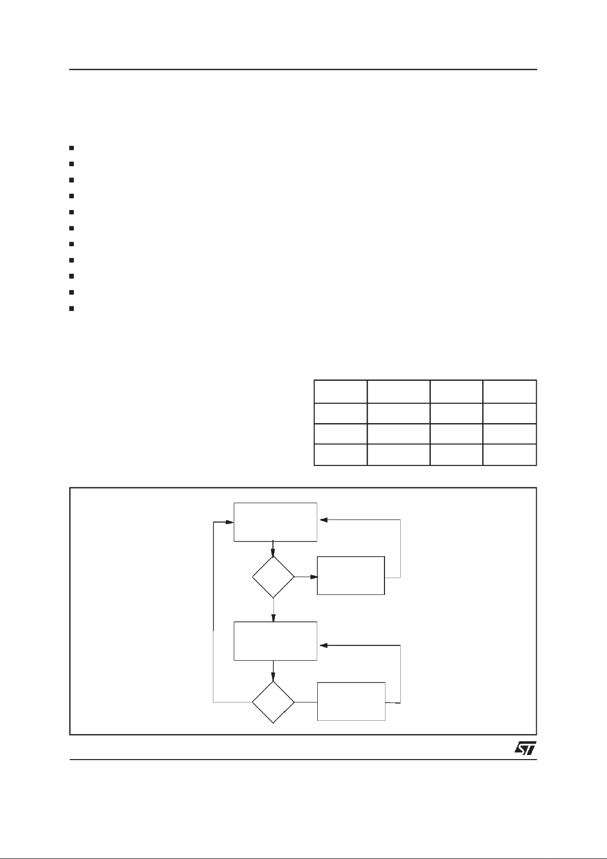
Control
Signal
Programming Reset Working
RESET
001
TEST
000
MODE
100
Table2.1.Control Signals setting
CU
Readsfromthe EPROM
and
Decodifies the instruction
CU
executesinstruction
FuzzyCore
Readsfromthe EPROM
and
Decodifies the instruction
STOP?
STOP?
No
No Fuzzy Core
executesinstruction
Yes
Yes
Figure2.1.ComputationAlgorithm FlowChart
6/99
ST52T301/E301
8 BIT
A/D CONVERTER
EPROM
2 KBytes
TIMER
TRES
TCLK
TIMEROUT
FUZZY CORE
I/O
PARALLEL PORT
P0..P7
AIN0..AIN3
POWER SUPPLY
OSCILLATOR
RESET
TRIAC/PWM
DRIVER
MAIN1
MAIN2
TRIACOUT
CONTROL
UNIT
RESETOSCinVSSVDD
ALU
PC
Register File
Input
Registers
INP_PORT
SCI_IN
SCI_ST
FUZZY_OUT_0
FUZZY_OUT_1
ADC_OUT_0
ADC_OUT_1
ADC_OUT_2
ADC_OUT_3
TMR_OUT
TMR_ADC_ST
VPP
Reg 0
Reg 15
Reg 1
REG_CONF0
REG_CONF15
REG_CONF1
Configuration
Registers
SCI
(UART)
TxD
TCTRL
RxD
FLAGS
P8
READY
OSCout
Peripheral
Register
PERIPH_REG_0
PERIPH_REG_1
PERIPH_REG_2
Figure2.2.ST52x301BlockDiagram
7/99
ST52T301/E301

It isnot possibileto stopthe fuzzy inferencebefore
theendof thedefuzzificationof one output.Aset of
26 different arithmetic and logic instructions is
available.Eachinstructionrequiresfrom4 to7clock
pulsesto be performed.
2.1.1 ProgramCounter
TheProgramCounter(PC) is a 11-bit register that
containsthe address of the next memory location
tobe processed bythe core.This memory location
maybe anopcode,an operandoranaddressof an
operand.
The 11-bit length allows the direct addressing
modeof 2048 bytes in the program space.
After having read the current instruction address,
the PC value is incremented. To execute relative
jumpsthe PCand theoffset are shiftedthroughthe
Fuzzy Core or theALU, where they will be added.
The result ofthis operationis shifted backinto the
PC.
The PC can be changedin thefollowing ways:
JP (Jump) instruction PC= JumpAddress
Interrupt PC= InterruptVector
RETI instruction PC =Pop(stack)
Reset PC= Reset Vector
Normal Instruction PC= PC + 1
2.1.2 Flags
TheST52x301coreincludestwopairsof flagsthat
correspondto 2 differentmodes:normal mode and
interruptmode.Each pair consistof a CARRY flag
anda ZEROflag.Onepair (CN,ZN) is usedduring
normal operation and one is used during the
interruptmode (CI,ZI).
The ST52x301 core uses the pair of flags that
correspond to the actual mode: as soon as an
interruptis generated,the ST52x301core usesthe
interruptflagsinsteadof thenormalflags.Whenthe
RETI instruction is executed the normal flags are
restoredif theMCUwas in the normal modebefore
the interrupt. It shouldbe observed that each flag
setcan onlybe addressedin its ownroutine.
The flags are not cleared during the context
switching and remain in the state they were at the
exitof the last routine switching.
The Carry flag is set when a carry or a borrow
occursduring arithmeticoperations,otherwiseit is
cleared.
The switching between the two sets of flags is
automatically performed when an interrupt or a
RETI instructionoccur.
2.2 ADDRESS SPACES
W.A.R.P3TChas four separateaddressspaces:
RegisterFile:16 8-bitregisters
Input Registers:11 8-bit registers
ConfigurationRegisters:16 8-bit registers
PeripheralRegisters:3 8-bit registers
Programmemory up to 2K Bytes
The Program memory will be described in further
detail in the MEMORYsection
2.2.1 Register File
The Register File (RF) consists of 16 general
purpose8-bit registers Reg0 to Reg15.
Allthe registersin theRF can be specifiedby using
a decimal address,
e.g. 0 identify the first register of the RF, called
Reg0.
Reg0:3 are directly connectedto the FC input. It
meansthat the input values of the fuzzyalgorithm
mustbe loadedinto theseregisters bythe user.
These registers are used as temporary registers
duringthe macros’computation.
8/99
ST52T301/E301
Input Registers
ALU
LDRI
Register File
FUZZY
CORE
LDPR
LDRR
LDRC
LDCF
CORE ON-CHIP PERIPHERALS
P e r iph er al Reg ister s
Configuration
Registers
Program Mem ory
PERIPHERAL
BLOCK
LDCFCRi,x
(1)
Figure2.3. AddressSpaces description
RegisterFile
Reg0
Reg1
Reg2
Reg3
Reg4
Reg5
Reg6
Reg7
Reg8
Reg9
Reg10
Reg11
Reg12
Reg13
Reg14
Reg15
FUZZY_IN_0
FUZZY_IN_1
FUZZY_IN_2
FUZZY_IN_3
Free
Free
Free
Free
Free
Free
Free
Free
Free
Free
Fuzzy Core
Register Description
Free
Free
Figure2.4. RegisterFiledescription
9/99
ST52T301/E301
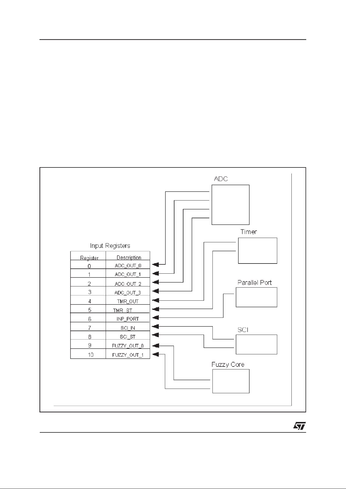
Figure2.5.Input Registers Bench description
2.2.2 Input Registers Bench
TheInput Registers(IR)bench consistsof 118-bit
regis ters co n tai ni ng dat a or statu s of t he
peripherals.
Alltheregisterscanbespecifiedbyusinga decimal
address,e.g.0 identifiesthe firstregister of theIR.
The first four registers (ADC_OUT_0:3) of the IR
are dedicated to the 4 converted values coming
fromthe ADC.
TMR_OUTregisters containsthe current counted
value by the internal Timer; whereas TMR_ST is
the Timer status. For details about TMR_ST,
pleaserefer toTimer description.
Data read by the Parallel I/O Port are stored
automaticallyin the 6-th register, INP_PORT.
Data read by the SCI are stored automatically in
the7-thregisterSCI_IN and SCI status is storedin
the SCI_ST register. For details about SCI_ST,
pleasereferto SCI description.
TheFuzzyCorewritesthe computedoutputvalues
in theFUZZY_OUT_0:1 registers.
10/99
ST52T301/E301
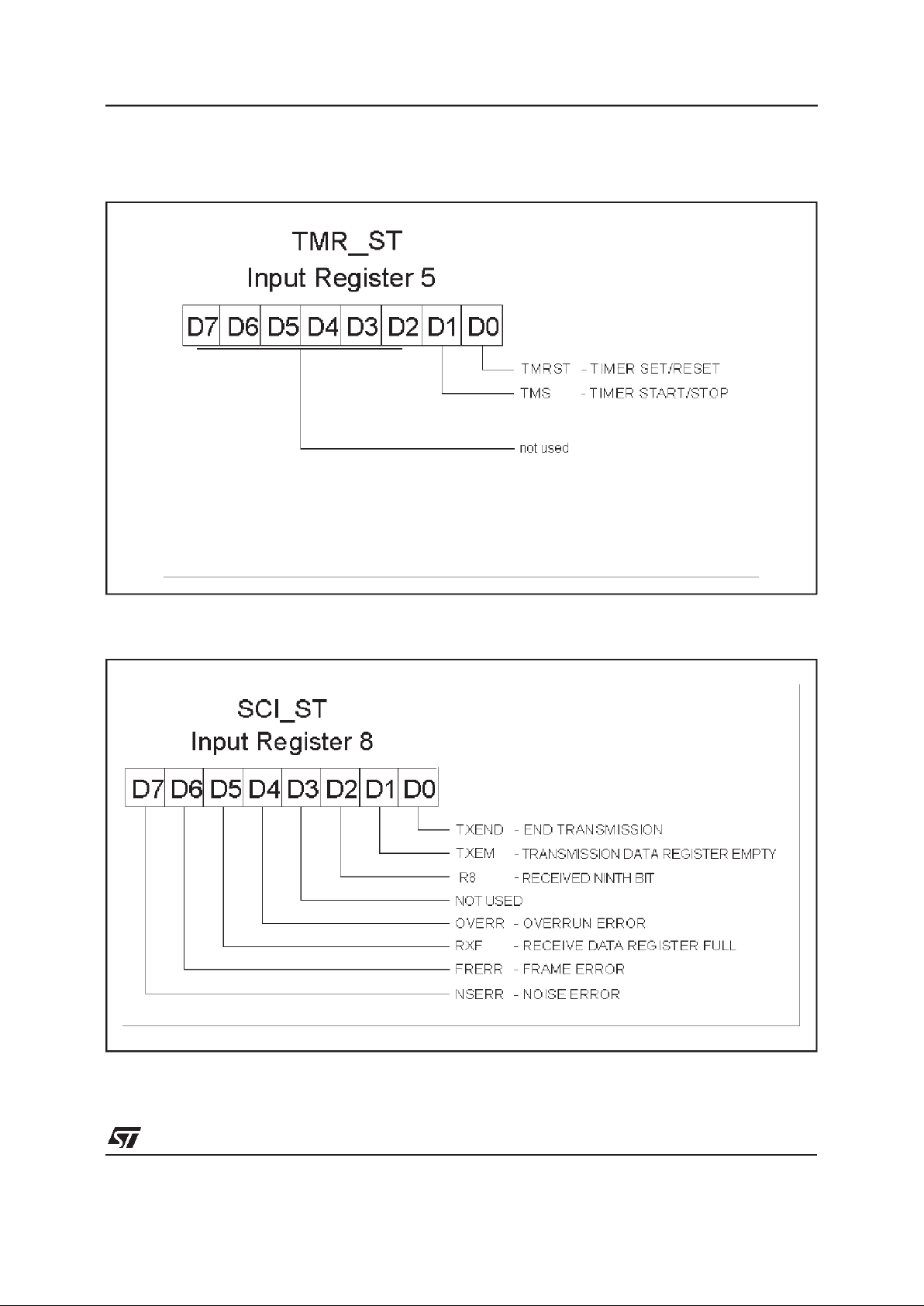
Figure2.6. TMR_ADC_STRegisters
Figure2.7.SCI_STRegisters
11/99
ST52T301/E301

2.2.3 Configuration Registers
The ST52x301 setting permits to configure all
blocks.Table2.2describestherelatedblocktoeach
bit of the ConfigurationRegisters.
Useandmeaningof eachregisterwillbedescribed
in furtherdetails in the corresponding section.
Register Peripheral Bit 7 Bit 6 Bit 5 Bit 4 Bit 3 Bit 2 Bit 1 Bit 0
REG_CONF0
PARALLEL
PORT
IO7 IO6 IO5 IO4 IO3 IO2 IO1 IO0
REG_CONF1
SCI, CORE,
I/O PORT
RDRF OVR BRK TDRE TXC ECKF P8 OUT
REG_CONF2
ADC
not used IADD 1 ADRST
REG_CONF3
SCI
BRSL T8 M RE TE
REG_CONF4
TIMER
TMLSB
REG_CONF5
TIMER
TMMSB
REG_CONF6
TIMER
notused POL TMS CKSL TMEL IESL TMST TMRST
REG_CONF7
TIMER
not used FZSL INPSL INTR INTF INTSL
REG_CONF8
TRIAC
TCLSB
REG_CONF9
TRIAC
TCMSB
REG_CONF10
TRIAC
IOSL PSF CKSL MODE TCST TCRST
REG_CONF11
TRIAC
INTSL TCMSK TCTRS POL
REG_CONF12
TRIAC
FZSL INPSL UTPMSB
REG_CONF13
TRIAC
UTPLSB
REG_CONF14
INTERRUPT
EXTI not used MSKTC MSKTM MSKSCI MSKAD MSKE
REG_CONF15
INTERRUPT
INT4 INT3 INT2 INT1
Table 2.2. ConfigurationRegistersdescription
12/99
ST52T301/E301

2.2.4 PeripheralRegisters
Peripheral Registers contain the initialization
valuesforthe Timer,Triac/PWM DriverandParallel
Port.
The peripheral initialization value is kept from a
location of the Register File, by using a LDPR
instruction , or from FUZZY_OUT_0/1 Input
Register according with the related Configuration
Registers.
Table 2.3 describes therelated peripheral to each
ConfigurationRegister.
Useandmeaningof eachregisterwillbedescribed
in furtherdetails in the corresponding section.
Peripheral Register Peripheral
PERIPH_REG_0
Timer
PERIPH_REG_1
Triac/PWM Driver
PERIPH_REG_2
ParallelPort
Table2.3.Peripheral Register description
13/99
ST52T301/E301
2.4 FUZZY CORE
ST52x301Fuzzy Coremain featuresare:
Up to 4 Inputswith 8-bitresolution
Up to 16 Membership Functions(Mbfs) for each
Input (64 possibleMbfs)
Up to 2 Outputswith 8-bit resolution
Possibility to process fuzzy rules with a max.
numberof 8 antecedents
2.4.1 Internal Structure
The block diagram shown in figure 2.9 describes
thestructureofST52x301FuzzyCore.Inthisfigure
wecandistinguishdifferentfunctionalblocks:Alpha
Calculator, InferenceUnit and Defuzzifier. These
blocks allow to perform a MAMDANI type fuzzy
inferencewith crisp consequents.It is importantto
underline that the fuzzyinferenceis performedby
usingasinputsthe first4 locationsof theRegisters
File.
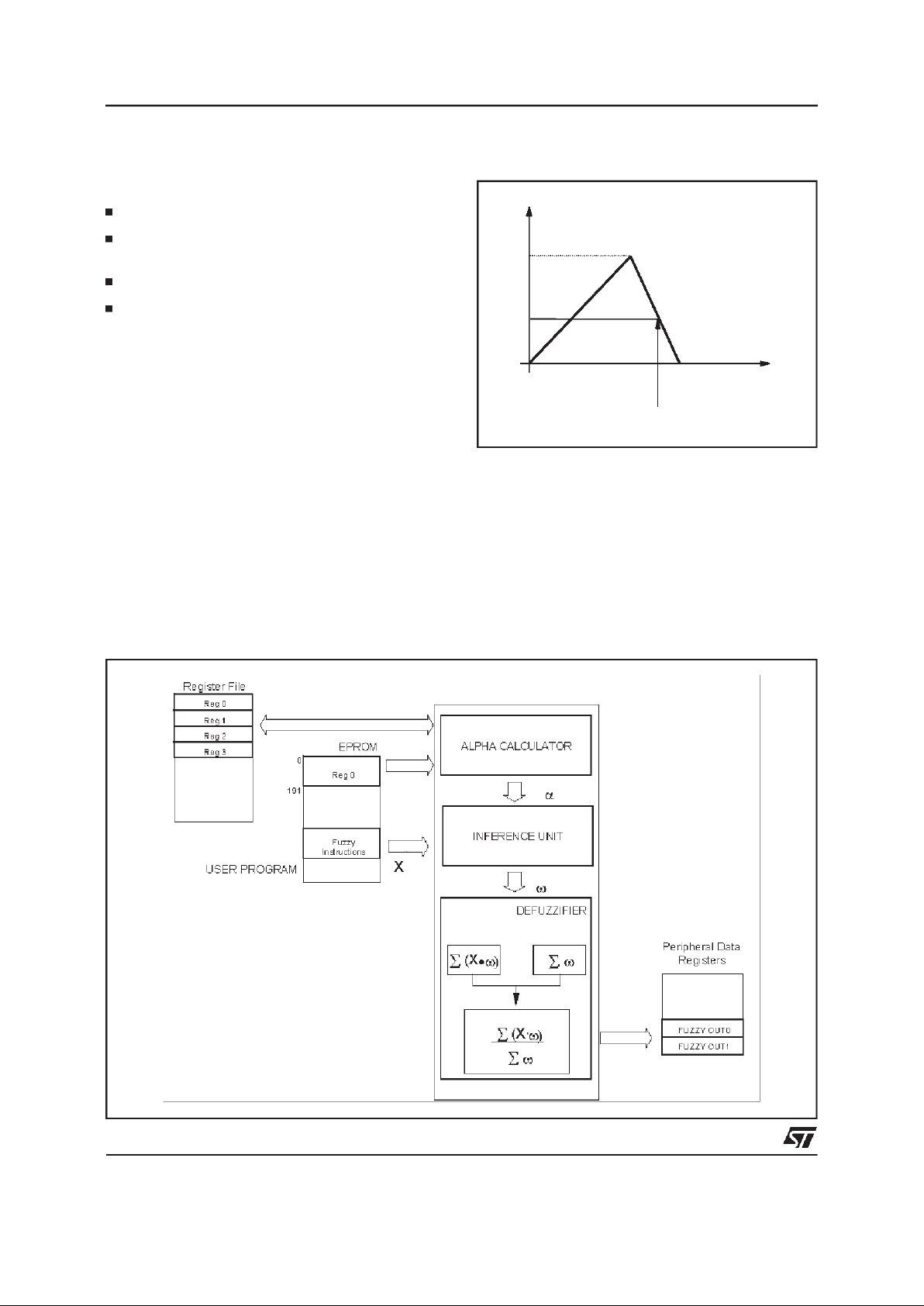
2.4.2 Alpha Calculator Unit
Thisblockperformstheintersection(alpha weight)
betweenthe input values and the relatedMbfs(fig.
2.8).
1
InputValue
α
ij
j-thMbf
i-th INPUT VARIABLE
Figure2.8.Alpha Weigthcalculation
Figure2.9.Fuzzy Core Block Diagram
Notice that the inputs for this blockcome from the
firstfourlocationsof the RegisterFile;it means the
user, to evaluate a fuzzy function, must load the
input valuesin theseregisters.
Alpha Calculator performs what is called
fuzzification
: the input data are transformed in
activationlevel (alpha weight) ofthe Mbfs.
14/99
ST52T301/E301
2.4.3 InferenceUnit
ItmanagesthealphaweightsobtainedbytheAlpha
CalculatorUnit to computethe truth value( ω ) for
each rule.
This is a calculation of the maximum (for the OR
operator) and/or minimum (for the AND operator)
performedon alpha valuesaccordingto the logical
connectivesof fuzzyrules.
It is possibileto linktogetherup to eight conditions
by linguistic connectives AND/OR, NOT operator
and brackets.
Each rule can have at maximum 8 alpha weights
(howevertheyare connected).
The truth value ω and the related output singleton
are passed to the Defuzzifier to complete the
inferencecalculation.
Input 1
X1
α1
Input 2
X2
α2
OR = Max
IF INPUT 1 IS X1 OR INPUT 2 IS X2 THEN.......
Input 1
X1
α1
Input 2
X2
α2
IF INPUT 1 IS X1 AND INPUT 2 IS X2 THEN.......
Figure2.10.
2.4.4 Defuzzifier
This block consists of a Multiplier,two Addersand
one Divider. It generates the output crisp values
implementingthe consequentpart ofthe rules.
In this phase each consequent Singleton X
i
is
multipliedby its weightvaluesω
i
, calculatedbythe
InferenceUnit in order to computethe upper part
of the defuzzification.
Eachoutputvalue(FUZZY_OUT0,FUZZY_OUT1)
is deduced from the consequentcrisp values (X
i
)
by using the defuzzificationformula:
Y
i
=
∑
X
ijωij
j
N
∑
ω
ij
j
N
where:
i = 0,1 identifies the current output variable
N= numberof theactiveruleson thecurrentoutput
ω
ij
=weigthof the j-th singleton
Xij= abscissaof the j-thsingleton
The two fuzzy outputsare stored in the location9
and 10 of the Input Registers (FUZZY_OUT_0,
FUZZY_OUT_1).
1
i-th OUTPUT
VARIABLE
0
X
ij
X
i0
X
in
ω
i0
ω
ij
ω
in
j-th Singleton
Figure 2.11.
15/99
ST52T301/E301

2.4.5 Input Membership Function
ST52x301 allows to manage triangular Mbfs. In
order to definea Mbfit is necessary tostore three
differentdata on thememory:
the vertex of the Mbf: V;
the lenght of the leftsemi-base:LVD;
the lenght of the rightsemi-base:RVD;
In order to reduce the dimension of the memory
area and the computational effort the vertical
dimensionof the vertexis fixed to 15 (4 bits)
By using the previous memorization method it is
possible to store different kinds of triangular
Memberships Functions. In the following figure is
shown a typical example of Mbfs that can be
definedin ST52x301
Each Mbf is then defined storing 3 bytes.To store
all the information related with the fuzzy project
Mbfs, it is necessary to use 192 bytes of the
memory(3 bytes*16Mbfs*4 Inputs = 192bytes).
X
15
LVD RVD
V
15
0
0
InputMbf
OutputSingleton
OutputVariable
InputVariable
w
Figure2.12.MbfsParameters Figure2.13.Exampleof valid Mbfs
The Mbf is memorized by using the following
instruction:
DATAn m lvdv rvd
where
n identifies the input, m identifies the Mbf among
the16 possibleMbfs,lvd,v, rvdare the parameters
describingthe Mbf’s shape.
2.4.6 Output Singleton
ST52x301usesfortheoutputvariablesa particular
kind of membership function called Singleton. A
Singleton has not a shape, like a traditional Mbf,
and it is characterized by a single point identified
by the couple (X, ω), where the ω is calculatedby
the Inference Unit asdescribedbefore.
Oftena Singletonis simply identifiedwith its Crisp
Value X.
16/99
ST52T301/E301

2.4.7 Fuzzy Rules.
The rules can havethe following structures:
if A op B op C...........thenZ
if (A op B)op ( C op D op E...) ...........thenZ
whereop isone of the possiblelinguisticoperators
(AND/OR)
In the first case the rule operators are managed
sequentially;in the second one,the priority of the
operatoris fixed by thebrakets.
Each rule is codifiedby using an istructionset, the
inferencetime for a rule with 4 antecedentsand 1
consequentis about3 microseconds.
TheassemblerInstruction Set allowingto manage
the fuzzy instructions arereported in the following
table:
Instruction Description
DATA n m lvd v rvd Stores the Mbf m of the input n with the shape identified by the parameters lvd, v and rvd.
LDP nm Fixesthe alpha value of the input n with the Mbf m and stores it in the data stack.
LDN n m
Calculates the negatedalpha value of the input n with the Mbf m and store the resultin the data
stack.
FZAND Implements the fuzzy operation AND between the last two values stored in thedata stack.
FZOR Implements the fuzzyoperationOR between the last two values stored inthe data stack.
LDK Stores the result of the lastfuzzy operation executed in thedata stack.
SKM Stores the result of the last fuzzy operationexecutedin the memory register M.
LDM Copies the valueof the register M in the data stack.
CON crisp
Multiplies the crisp valuewith the lastωweight.
OUT n_out Performs the defuzzification.
STOP
Ends the fuzzy algorithm.
Table 2.4. FuzzyInstructions Set
17/99
ST52T301/E301

Example1:
IF Input
1
IS NOTMbf1ANDInput4is Mbf12ORInput3IS Mbf8THENCrisp
1
is codified by the followinginstructions
LDN1 1
calculatesthe NOT α valueof Input
1
withMbf1and stores the resultin the data stack
LDP 4 12
fixesthe α valueof Input
4
withM12and stores the resultin the data stack
FZAND
adds the NOTα andα valuesobtainedwith the operations LDN1 1 andLDP 4 12
LDK stores the resultof the operation FZAND inthe data stack
LDP 3 8
fixesthe α valueof Input
3
withMbf8and stores the resultin thedata stack
FZOR implementsthe operationOR betweenthe resultsobtainedwith the operationsLDK
and LDP
CON crisp
1
multiplies the resultof the lastΩ operationwith the crispvalue Crisp
1
Example2, the priority of the operator is fixedby thebrakets:
IF (Input
3
IS Mbf1ANDInput4IS NOTMbf15) OR(Input1IS Mbf6OR Input6IS NOTMbf14) THEN Crisp
2
LDP 3 1
fixesthe α valueof Input
3
withMbf1and stores the resultin the data stack
LDN4 15
calculatesthe NOT
α valueof Input4withMbf15and stores the resultin the data
stack
FZAND
adds NOT α and α values obtained with the operations LDP 3 1 and LDN4 15
SKM storesthe result of theoperationFZAND in the memory registerM
LDP 1 6
fixesthe α valueof Input
1
withMbf6and stores the resultin the data stack
LDN2 14
calculatesthe NOT
α valueof Input6withMbf14and stores the resultin the data
stack
FZOR
implementsthe operationOR betweenthe α and NOT α valuesobtainedwith the
two previous operations(LDP 1 6 andLDN 2 14)
LDK stores the resultof the operation OR in the data stack
LDM copies the value of the memoryregisterM in the data stack
FZOR implementsthe operationOR betweenthe last two valuesstored in the data stack
(LDK and LDM)
CON crips
2
multiplies the resultof the lastΩ operationwith the crispvalue Crip
2
At theend of thefuzzy rules set a byte,to identify
the output involved in the rules, and the STOP
istructionmustbe inserted.
When the STOP instruction is performed, the
controlof thealgorithmgoes backto the CU.
18/99
ST52T301/E301

2.5 ARITHMETICLOGIC UNIT
The 8-bit Arithmetic Logic Unit (ALU) allows to
perform arithmetic calculations and logic
instructions which can be divided into 4 groups:
Load, Arithmetic, Jump and Program Control
instructions(refer to the ST52x301AssemblerSet
forfurther details).
Load Instructions
Menmonic Instruction Bytes Cycles Z S
LDCF LDCF conf,const 2 6 - -
LDRC LDRC reg, const 2 6 - -
LDRI LDRI reg, inp 2 6 - LDPR LDPR per, reg 1 6 - LDRR LDRR regi, regj 2 6 - -
Arithmetic Instructions
Mnemonic Instruction Bytes Cycles Z S
ADD ADD regi, regj 2 7 I I
AND AND regi, regj 2 7 I SUB SUB regi, regj 2 7 I I
SUBO SUBOregi, regj 2 7 I I
Jump Instructions
Mnemonic Instruction Bytes Cycles Z S
JP JP addr 2 6 - JPNS JPNS addr 2 6 - JPNZ JPNZ addr 2 6 - -
JPS JPS addr 2 6 - JPZ JPZ addr 2 6 - -
SCI Instructions
Mnemonic Instruction Bytes Cycles Z S
SRX SRX regi 2 5 - -
STX STX regi 2 5 - -
Notes:
I affected
- notaffected
Table 2.5. Arithmetic& LogicInstructionsSet
The computational time required for each
instruction consists of one clock pulse for each
Cycleplus 3 clockpulses for the decoding phase.
19/99
ST52T301/E301

Program ControlInstructions
Mnemonic Instruction Bytes Cycles Z S
RETI RETI 1 5 I I
RINT RINT int 1 4 - STOP STOP 1 4 - WAITI WAITI 1 4 - -
UDGI UDGI 1 4 - -
UEGI UEGI 1 4 - -
MDGI MDGI 1 4 - MEGI MEGI 1 4 - -
IRQ IRQ int label 2 6 - -
IRQM IRQM mask 2 6 - -
IRQP IRQP cost 2 6 - -
Notes:
I affected
- notaffected
Table 2.6. Arithmetic& LogicInstructionsSet (Continue)
20/99
ST52T301/E301

3 EPROM
The EPROM memory provides an on-chip
user-programmable non-volatile memory, that
allowsfastand reliable storage of userdata.
Thereare 16K bitsof memory spacewith an 8-bit
internal parallelism (2Kbytes) addressed by an
11-bitbus.The data bus is of 8 bits.
The memory has a doublesupply:V
PP
is equalto
12V±5% in Programming Phase and 5V±10%
duringWorkingPhase.V
DD
is equalto 5V±10%.
The EPROM memory of ST52x301 is divided in
three main blocks (see Figure3.1):
Mbfs Setting with (0 through 191) contains the
coordinatesof the vertexesof everyMbf defined
in theprogram.
Interrupt Vectors (192 through 201) contain the
addressesfor the interruptroutines.
Each address is composedof twobytes.
Program Instruction Set (202 through 2048)
containsthe instructionset of theuser program.
It canbe composed of moreBooleanand Fuzzy
Algorithms
The operation that can be performed, during
Programming Phase,on the EPROMare:Writing,
Verify,Writing Inhibit,Standbyand Erasing.
Figure 3.2 shows the signals timin g in
Programming Mode.
0
192
191
202
201
2048
Mbfs Setting
InterruptVectors
Program
InstructionsSet
Boolean Algorithm
Boolean Algorithm
FuzzyAlgorithm
FuzzyAlgorithm
······
INT_EXT
INT_TRIAC
INT_TIMER
INT_SCI
INT_ADC
Mbf Parameters
Figure3.1.MemoryMap
3.1 EPROM ProgrammingPhase Procedure
Programming mode is selected by applying
12V±5% voltage to the V
PP
pin and set the control
signalas following:
RESET:0, TEST:0, MODE:1.
CADD, ERES, OE and CE are the control signals
used during the Programming Mode. CADD is
activeon edge,the othersare active onlevel(OE,
CE are activelow,ERES is activehigh).
3.1.1EPROMWriting
Whenthe memoryis blank,all thebits are at logic
level”1”.The dataareintroducedby programming
only the zeros in the desired memory location;
however all input data must contain both ”1” and
”0”.
Theonly wayto change ”0” into ”1”is to erase the
whole memory ( by exposure to Ultra Violet light)
and reprogramit.
Thememory is in Writing modewhen:
CE = LOW
OE= HIGH
withstabledata on the databus P(0:7).
The total programming pulse width (CE = 0 V) is,
typically,50 µs (bymeansof 5pulsesof 10µs),but
beforeactivatingsuch pulse,it is suggestedto wait
for at least 2 µs after V
PP
rises at 12 V .After the
disactivationof the pulse it issuggestedto wait for
21/99
ST52T301/E301
at least 2 µs before updating the data and the
address.
The data updating for the next programming is
performed, directly by the user, on the data bus
P(0:7) while the address is incremented through
the pin CADD.
3.1.2EPROMVerify
A Verify mode is available in order to verify the
correctness of the data written. It is possible to
activate the Verify mode immediately after the
writing of eachbyte:
CE = HIGH
OE= LOW
Then, ifany error in writing occured, the user has
to repeat the EPROMwriting.
The data, during this phase, are avalaible on the
busP(0:7)
3.1.3WritingInhibit
It occursbetween the Writing and Verify Mode:
CE = HIGH
OE= HIGH
3.1.4 Standby Mode
The EPROM has a standby mode which reduces
theactivecurrentfrom10mA(Programmingmode)
to less than 100 µA. The Memory is placed in
standbymode by setting CE at HIGH Logic Level
(V
PP
might be equal to 5 V too).When in standby
mode,the outputs are in highimpedancestate.
3.2 Eprom Erasure
Thanks to the transparent window present in the
CLCC44-Wpackage,its memory contentsmaybe
erasedby exposureto UV light.
Erasurebeginswhenthedeviceisexposed to light
witha wavelengthshorterthan4000Å.It shouldbe
noted that sunlight, as well as some types of
art ificia l light, includes wavelength s in the
3000-4000Årange which, onprolongedexposure,
can cause erasure of memory contents.It is thus
recommended that EPROM devices be fitted with
an opaquelabel over the window area in orderto
preventunintentionalerasure.
Therecommendederasure procedureforEPROM
devicesconsistsof exposureto shortwaveUVlight
having a wavelength of 2537Å. The minimum
recommende d integrat ed dose (intens ity x
expo-su re time) f or co mplete erasure is
15Wsec/cm2 .
This is equivalent to an erasure time of 15-20
minutesusing a UV source having an intensityof
12mW/cm 2 at a distance of 25mm (1 inch) from
the device window.
OE
P(0:7)
DATA IN
VPP
5V
12V
CE
Inhibit
min 2us
2us typ.
DATA OUT
RESET
CADD
Writing Verify
ERES
INPUT
PORT
50us typ.
OUTPUT
PORT
3us min.
Figure3.2.EPROMProgrammingTiming
22/99
ST52T301/E301

4 INTERRUPTS
The Control Unit (CU) responds to peripheral
events and external events through its interrupt
channels.
Whensuch an eventoccurs,if itisnot maskedand
according to a priority order, the current program
execution can be suspended to allow the CU to
executea specificresponseroutine.
Eachinterruptisassociatedwithaninterruptvector
that contains the memory address of the related
interrupt service routine.Each vector is located in
the Program Space (EPROM Memory) at a fixed
address(seeInterrupt Vectorstable fig.4.2).
4.1 Interrupt Functionment
If, at the end of an arithmetic or logic instruction,
there are pending interrupts, the one with the
highest priority is passed. To pass an interrupt
meansto storethe arithmeticflagsand the current
PC in the stack and execute the associated
Interrupt routine, whose address is located in one
of theEPROMmemory location betweenaddress
192 and 201.
TheInterruptroutineisperformedasanormalcode
checking,at theendof eachinstruction,if a higher
priority interrupt has to be passed. An Interrupt
request with the higher priority stops the lower
priority Interrupt. The Program Counter and the
arithmeticflags are storedin the stack.
With the instruction RETI (Return from Interrupt)
thearithmeticflagsand ProgramCounter(PC)are
restoredfrom the topof thestack.Thisstack,used
forthe Interrupt priority, is a LIFOqueue.
AnInterruptrequest cannotstop the processingof
the fuzzy rules but this is passed only after the
definitionof thefuzzyoutputorattheendof a logic
or arithmetic instruction.
4.2 Global InterruptRequestEnabling
When an Interrupt occurs, it generates a Global
InterruptPending(GIP), that can be hangedup by
software.After a GIP a Global Interrupt Request
(GIR) will be generate and Interrupt Service
Routine associated to the interrupt with higher
prioritywill start.
In order to avoid possible conflicts between
interruptmaskingset inthemainprogramor inside
macros, the GIP is hanged up through the User
GlobalInterrupMask or the MacroGlobalInterrup
Mask (see fig.4.3).
UEGI/UDGI instruction switches on/off the User
GlobalInterrupMaskenabling/disablingtheGIRfor
the main program.
MEGI/MDGI instructions set the Macro Global
InterruptMaskinorder toassurethatthe macrowill
not be broken.
NORMAL
PROGRAM
FLOW
INTERRUPT
SERVICE
ROUTINE
RETI
INSTRUCTION
INTERRUPT
Figure4.1.Interrupt Flow
InterruptVectorsINT_TIMER
198
196
200
199
197
195
194
193
192
191
INT_SCI
INT_ADC
INT_TRIAC
INT_EXT
202
201
Figure4.2.Interrupt VectorsMapping
Global Interrupt
Pending
User Global
InterruptMask
Macro Global
InterruptMask
Global Interrupt
Request
Figure4.3.Global Interrupt Request generation
23/99
ST52T301/E301

4.3 Interrupt Sources
ST52x301managesinterruptsignalsgeneratedby
the internal peripherals (Timer, Triac/PWM
Driver,Analog to Digital Converter and Serial
CommunicationPort) orcomingfrom the INT pin.
The polarity of the External Interrupt is
programmedby the EXTIbit of theREG_CONF14
(see Table 4.1 and fig. 4.4). EXTI=0 means that
INT_EXT is active on rising edge, otherwise it is
activeon fallingedge.
Each peripheral can be programmed in order to
generatethe associateinterrupt;furtherdetailsare
describedin therelatedchapter.
4.4 Interrupt Maskability
The interrupts can be masked by configuring the
REG_CONF14.The interruptis enabledwhen the
bit associated to the mask interrupt i s ”1”.
Viceversa, when the bit is ”0”, the interrupt is
maskedand is keptpendent.
ForexampleLDCF 14, 6
(CONF_REG14 =00000110) enables interrupts
comingfromtheADC(INT_ADC)and fromtheSCI
(INT_SCI).
4.5 Interrupt Priority
Six priority levels are available: level 5 has the
lowestpriority,level0 hasthe highestpriority.
Level5 isassociatedtothe MainProgram,levels4
to 1 are programmable by means of the priority
register called RE G_CONF15 (see fig.4.5);
whereas the higher levelis related to the external
interrupt(INT_EXT).
Timer, Triac/PWM Driver, SCI and ADC are
identifiedby a twobitsPeripheralCode (see Table
4.2); in order to set the
i
-th priority level the user
must write the peripheral label
i
in therelatedINT
i
prioritylevel.
Bit Name Value Description
0 MSKE
0
External Interrupt
Masked
1
External Interrupt
Not Masked
1 MSKAD
0
A/D ConverterInterrupt
Masked
1
A/D ConverterInterrupt
Not Masked
2 MSKSCI
0
SCI Interrupt
Masked
1
SCI Interrupt
Not Masked
3 MSKTM
0
TIMER Interrupt
Masked
1
TIMER Interrupt
Not Masked
4 MSKTC
0
TRIAC/ PWM Interrupt
Masked
1
TRIAC/ PWM Interrupt
Not Masked
5 not used 6 not used -
7 EXTI
0
Activeon Rising Edge
1
Activeon Falling Edge
Table4.1.ConfigurationRegister 14 Description
Name Description Priority
Peripheral
Code
Maskable
EPROM
Locations
INT_EXT ExternalInterrupt (INT)
Ext Highest - yes 200-201
INT_ADC ADC
Int Programmable 00 yes 192-193
INT_SCI SCI
Int Programmable 01 yes 194-195
INT_TIMER TIMER
Int Programmable 10 yes 196-197
INT_TRIAC TRIAC
Int Programmable 11 yes 198-199
Table 4.2. InterruptsDescription
24/99
ST52T301/E301

D7
D6 D5 D4 D3 D2 D1 D0
REG_CONF14
Interrupt
MSKE - ExternalInterrupt Mask
MSKAD - ADC Interrupt Mask
EXTI - ExternalInterrupt Polarity
MSKSCI - SCIInterrupt Mask
MSKTM - TIMERInterrupt Mask
not used
not used
MSKTC - TRIACInterruptMask
Figure4.4.InterruptConfigurationRegister14
D7
D6 D5 D4 D3 D2 D1 D0
REG_CONF15
Interrupt
INT1 - HIGH Level Interrupt
INT2 - MEDIUM-HIGH Level Interrupt
INT3 - MEDIUM-LOW Level Interrupt
INT4 - LOW Level Interrupt
Figure4.5.InterruptConfigurationRegister15
25/99
ST52T301/E301
i.e. LDCF 15, 201 (REG_CONF15=11001001)
definethe followingpriority levels:
Level1: INT_SCI(SCICode: 01)
Level2: INT_TIMER(TIMER Code:10)
Level3: INT_ADC(ADCCode:00)
Level4: INT_TRIAC(TRIACCode: 11)
Whena sourceprovidesan Interruptrequest,and
the request processing is also enabled, the CU
changes the normal sequentialflow of a program
bytransferingprogramcontrol toa selectedservice
routine.
Whenan interruptoccurs theCUexecutesa JUMP
instruction to the address loaded in the related
locationof the InterruptVector
Whentheexecutionreturnstotheoriginalprogram,
it begins immediately following the interrupted
instruction.
4.6 Interrupt RESET
An eventuallypending interruptscan be resetwith
the instruction RINT int
i
which resets thei-th
interrupt
Bit Name Value Level
0, 1 INT1
Peripheral
Code
High
2, 3 INT2
Peripheral
Code
Medium-High
4, 5 INT3
Peripheral
Code
Medium-Low
6, 7 INT4
Peripheral
Code
Low
Table4.3.ConfigurationRegister 15 Description
Figure4.6.Exampleof a Sequenceof InterruptRequests
26/99
ST52T301/E301
5 CLOCK
ST52x301 can work by using a 5, 10 or 20 MHz
clock.
TheST52x301 ClockGeneratormodule generates
theinternalclock for theinternal ControlUnit,ALU,
Fuzzy Core and on-chip peripherals and it is
designed to require a minimum of external
components.
Thesystemclockmaybegeneratedbyusingeither
a quartz crystal, or a ceramic resonat or
(CERALOC);or, at least, by means of an external
clock.
The different clock generator options connection
methodsare shown inFigure 5.1.
When an external clock is used, it must be
connectedonthepinOSCinwhileOSCoutmustbe
grounded.
The crystal oscillator start-uptime is a function of
manyvariables:crystalparameters(especiallyR
S
),
oscillator load capacitance (CL), IC parameters,
ambienttemperature,supplyvoltage.
It must be observed that the crystal or ceramic
leads and circuit connectionsmust be as short as
possible.Typical values for CL1, CL2are 10pF for
a 20MHzcrystal.
Figure5.1.OscillatorConnections
27/99
ST52T301/E301
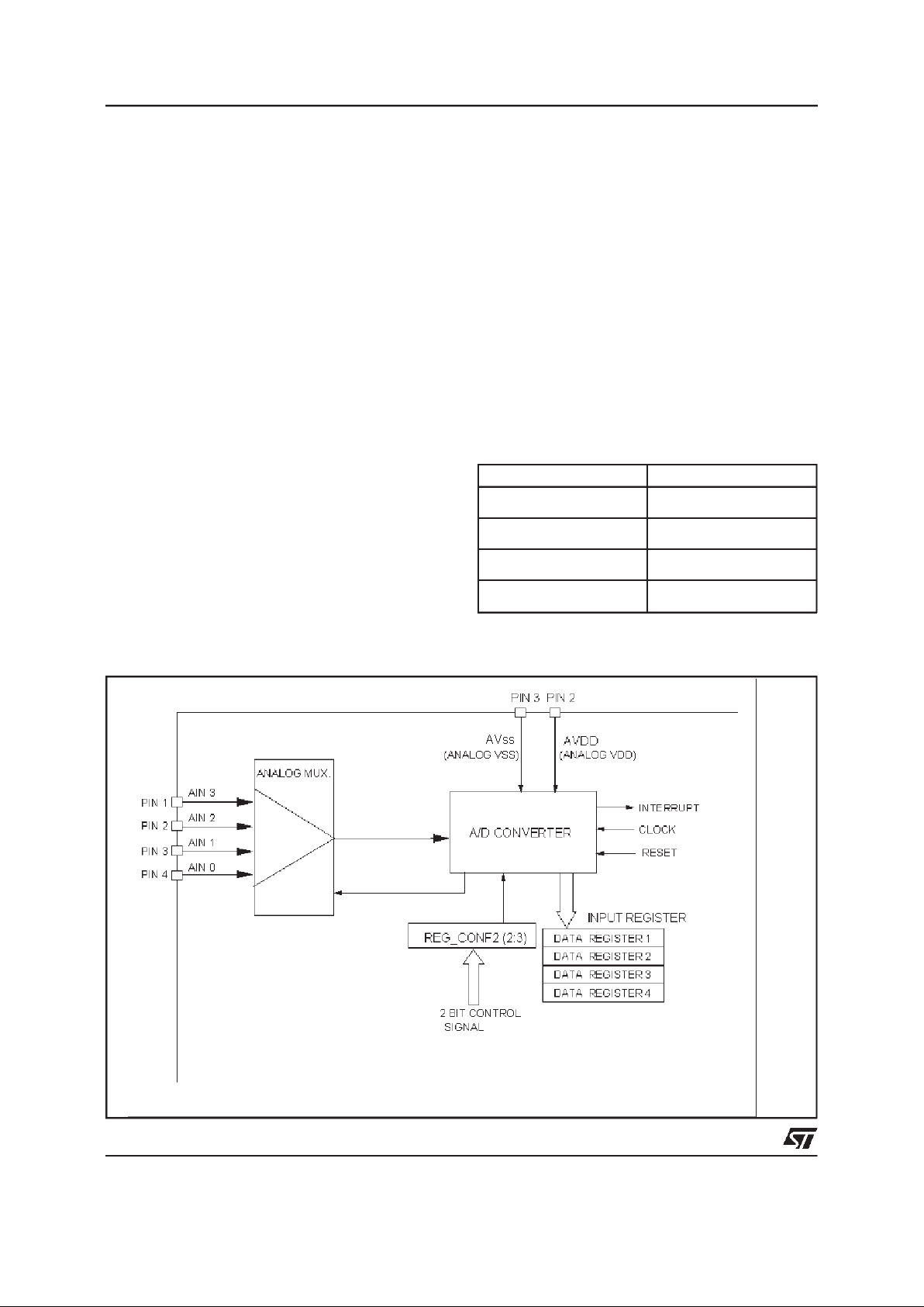
6. A/D CONVERTER
TheA/D Converter ofST52x301is an8-bitanalog
to digital converter with up to 4 analog inputs
offering8 bit resolution with a total accuracy of 2
LSB and a typical conversiontime of 32 µs.
Theconversionrange is 0 - 2.5V.
TheA/D peripheralconverts theinputvoltagewith
a process of successive approximations using a
fixedclock frequencyderived fromthe oscillator.
The ADC uses 5 registers: one Configuration
Register, REG_CONF2, and four Data Registers.
These4 registersare the first4 InputRegisters.
The A/D converterdrives theanalogMultiplexerin
order to sequentiallypickup the external inputs to
be put in output and storedautomaticallyin 4 8-bit
registers.
ItispossibiletoconfiguretheMultiplexerbymeans
of the registerREG_CONF2,in orderto select the
numberof analoginputs to convert.
Forexample,if thebit 3 andbit 2 of REG_CONF2
are configured at 10, then the Multiplexer will
sequentiallypickup only theinputs 0,1 and 2.
Table 6.1 shows the convertion sequences
according to the possible values of the two bit
REG_CONF2(3:2).
The A/D Converter,at the end of the conversion,
willsend a signal(end-of-conversion)whichcanbe
used like an interrupt signal. The user can select
the priority of the A/D interrupt and mask it (see
”InterruptRoutine”chapter)
The conversion start s writing ”1” on
REG_CONF2(0).The A/Dis resetby writing ”0” in
REG_CONF2(0).
Theconverteddataare automaticallystoredin four
8-bit Input Registers.
By performingan instruction:
LDRI regj ingi
theanaloginput”ingi”is loadedintheregister”regj”
of the RegisterFile.
Figure6.1.A/D Converter Structure
CONF_REG2 (3:2) INPUT SEQUENCE
00
Ain0
01
Ain 0, Ain1
10
Ain 0, Ain1, Ain 2
11
Ain 0, Ain1, Ain 2, Ain 3
Table6.1.
28/99
ST52T301/E301

The power consumption of the device can be
reducedby turning off the A/Dconverter,
ToswitchofftheA/DconvertertheCONF_REG2(0)
bit must bereset to ”0”.
The A/D Converter features a sampleand hold.
The input voltage Ain, which has to be converted
must be constant,for 12.8 µs.
An internal bandgap reference is available on pin
44, BG. By using this signal as reference for the
signalto be converted,theconversionaccuracy is
not strongly related withthe variation of the power
supply.
The power supplyof the A/D converter (AV
DD
and
AV
SS
) in orderto avoidinterferencesis mantained
separatedfromthe powersupplyof thedigitalcore.
D7 D6 D5D4 D3 D2D1 D0
ADC
Configuration Register
REG_CONF2
Reset ADC
Must be1
ADC inputselection
Not used
Figure6.2.ConfigurationRegister REG_CONF2
29/99
ST52T301/E301

7.TIMER
ST52x301 offers one on-chip Timer peripheral.
TheTimerconsists of an 8-bit counterwith a 16-bit
programmable prescaler, thus giving a maximum
count of 2
24
, an d c ontrol logic that allows
configuring the functionment and the type of
peripheral outputs. Figure 7.2 shows the Timer
block diagram and Figure 7.3 shows the internal
structureof the Timer.
Thecontentof the 8-bitcountercanberead/written
andis incrementedon the RisingEdge of the16-bit
prescaleroutput(PRESCOUT).Moreover,itcan be
read under program control at any instant of the
counting phase and loaded in a location of the
RegisterFile.Theprescalercanbe givenanyvalue
between 0 and FFFFh setting the 4-th (TMLSB)
and 5-th (TMMSB) locations of the Configuration
RegistersBench.
7.1TimerFunctionment
TheTimer requires three signals:TMRCLK,TRST
andTSTART(seeFigure7.3).Eachofthemcanbe
generatedinternallyor externally,this possibility is
programmableby the user.
TMRCLK increments the counted value of the
Pre sc a ler. It can be, by se tt in g C KSL of
REG_CONF6 register, the internal clock signal
(CLKM)or the signalprovidedon the pinTCLK.
TRSTresetsto zerothe contentofthe8bit counter.
It is generated by the TRES or RESET external
signalsoritisforcedbyTMRSTbitofREG_CONF6
register.
TSTARTstarts/stopsthePrescalercounting.It can
be given on the pin TCTRL orit isforcedby TMST
bit of REG_CONF6register.
The TSTART signalallows to work in two different
modes:
LEVEL (Time Counter)
: If the TSTART signal is
hightheTimerstarts thecount.WhentheTSTART
islow the count is stoppedand thecurrent valueis
stored in the TMR_OUT register of the Input
registerBench,thenit can betransferredtothe j-th
location of the Registers File by using the
instruction:
LDRI reg-j 4
EDGE(Period Counter)
: Afterthe reset,when the
firstedge oftheTSTARTsignalappears,theTimer
starts the count,at the next TSTART the Timer is
stopped.In this way it is possible to measure the
periodof an external signal.
The functionment modality is set by the TMEL
configurationbit of REG_CONF6register.
The starting value of the Counter can be either a
value contained in the Register File or directly a
FuzzyOutput.If INPSL(REG_CONF7(3))is set to
”1”thenthe value comes from oneof the locations
of the Register File (LDRP 0, reg-i); on the
contrary it is generated by the Fuzzy Core. The
choice between the two possible fuzzy outputs is
set by the FZSL configurationbit of REG_CONF6
register
FZSL=0/1 means the starting value is the loaded
fromthe FUZZY_OUT_0/1.
Level
Edge
start stop
start
start
stop
start
00 033321
Reset
Clock
Counted
Value
Figure7.1.Timer Functionalities
30/99
ST52T301/E301
 Loading...