

SGS Thomson Microelectronics ST52F513, ST52F510, ST52F514 Datasheet
®
ST52F510/F513/F514
8-BIT INTELLIGENT CONTROLLER UNIT (ICU)
Two Timer/PWMs, ADC, I2C, SPI, SCI
Memories
■ Up to 8 Kbytes Single Voltage Flash Memory
■ 256 bytes of Register Fi le
■ 256 bytes of RAM
■ Up to 4 Kbytes Data EEPROM
■ In Situ Programming in Flash devices (ISP)
■ Single byte and Page modes and In Application
Programming for writing data in Flash memory
■ Readout protection and flexible write protection
Core
■ Register File based architecture
■ 107 basic instructions
■ Hardware multiplication and division
■ Decision Processor for the implementation of
Fuzzy Logic algorithms
■ Deep System and User Stacks
Clock and Power Supply
■ Up to 24 MHz clock frequency
■ Programmable Oscillator modes:
– 10 MHz Internal Oscillator
– External Clock/ Oscillator
– External RC Oscillator
■ Power-On Reset (POR)
■ Programmable Low Voltage Detector (PLVD)
with 3 configurable thresholds
■ Power Saving features
Interrupts
■ 8 interrupt vectors with one SW Trap
■ Non-Maskable Interrupt (NMI)
■ Two Port Interrupts with up to 16 sources
I/O Ports
■ From 10 up to 22 I/O PINs configurable in pull-
up, push-pull, weak pull-up, open-drain and
high-impedance
■ High current sink/source in all pins
ST52F510/F513/F514
TARGET SPECIFICATION
Peripherals
■ On-chip 10-bit A/D Converter with 8 channel
analog multiplexer and Autocalibration.
■ 2 Programmable 16 bit Timer/PWMs with
internal 16-bit Prescaler featuring:
– PWM output
– Input capture
– Output compare
– Pulse generator mode
■ Watchdog timer
■ Serial Communication Interface (SCI) with
asynchronous protocol (UART).
2
■ I
C Peripheral with master and slave mode
■ 3-wire SPI
Master and Multi Master SPI modes
Development tools
■ High level Software tools
■ ‘C’ Compiler
■ Emulator
■ Low cost Programmer
■ Gang Programmer
Peripheral supporting Single
Rev. 1.18 -June 2003 1/106
This is preliminary information on a new product foreseen to be developed. Details are subject to change without notice.

ST52F510/F513/F514
2/106

ST52F510/F513/F514
TABLE OF CONTENTS
TABLE OF CONTENTS
1 GENERAL DESCRIPTION. . . . . . . . . . . . . . . . . . . . . . . . . . . . . . . . . . . . . . . . . 7
1.1 Introduction. . . . . . . . . . . . . . . . . . . . . . . . . . . . . . . . . . . . . . . . . . . . . . . . . . . . . . . . . . . . . . . . . . .7
1.2 Functional Description . . . . . . . . . . . . . . . . . . . . . . . . . . . . . . . . . . . . . . . . . . . . . . . . . . . . . . . . . .8
1.2.1 Memory Programming Mode . . . . . . . . . . . . . . . . . . . . . . . . . . . . . . . . . . . . . . . . . . . . . . . . 8
1.2.2 Working Mode. . . . . . . . . . . . . . . . . . . . . . . . . . . . . . . . . . . . . . . . . . . . . . . . . . . . . . . . . . . . 8
1.3 Pin Description . . . . . . . . . . . . . . . . . . . . . . . . . . . . . . . . . . . . . . . . . . . . . . . . . . . . . . . . . . . . . . .16
2 INTERNAL ARCHITECTURE. . . . . . . . . . . . . . . . . . . . . . . . . . . . . . . . . . . . . . 17
2.1 Control Unit and Data Processing Unit . . . . . . . . . . . . . . . . . . . . . . . . . . . . . . . . . . . . . . . . . . . . .17
2.1.1 Program Counter . . . . . . . . . . . . . . . . . . . . . . . . . . . . . . . . . . . . . . . . . . . . . . . . . . . . . . . . 18
2.1.2 Flags. . . . . . . . . . . . . . . . . . . . . . . . . . . . . . . . . . . . . . . . . . . . . . . . . . . . . . . . . . . . . . . . . . 18
2.2 Arithmetic Logic Unit. . . . . . . . . . . . . . . . . . . . . . . . . . . . . . . . . . . . . . . . . . . . . . . . . . . . . . . . . . .19
2.3 Register Description . . . . . . . . . . . . . . . . . . . . . . . . . . . . . . . . . . . . . . . . . . . . . . . . . . . . . . . . . . .20
3 ADDRESSING SPACES. . . . . . . . . . . . . . . . . . . . . . . . . . . . . . . . . . . . . . . . . . 21
3.1 Memory Interface . . . . . . . . . . . . . . . . . . . . . . . . . . . . . . . . . . . . . . . . . . . . . . . . . . . . . . . . . . . . .21
3.2 Register File . . . . . . . . . . . . . . . . . . . . . . . . . . . . . . . . . . . . . . . . . . . . . . . . . . . . . . . . . . . . . . . . .21
3.3 Program/Data Memory . . . . . . . . . . . . . . . . . . . . . . . . . . . . . . . . . . . . . . . . . . . . . . . . . . . . . . . . .21
3.4 System and User Stacks. . . . . . . . . . . . . . . . . . . . . . . . . . . . . . . . . . . . . . . . . . . . . . . . . . . . . . . .23
3.5 Input Registers . . . . . . . . . . . . . . . . . . . . . . . . . . . . . . . . . . . . . . . . . . . . . . . . . . . . . . . . . . . . . . .24
3.6 Output registers . . . . . . . . . . . . . . . . . . . . . . . . . . . . . . . . . . . . . . . . . . . . . . . . . . . . . . . . . . . . . .24
3.7 Configuration Registers & Option Bytes . . . . . . . . . . . . . . . . . . . . . . . . . . . . . . . . . . . . . . . . . . . .25
4 MEMORY PROGRAMMING. . . . . . . . . . . . . . . . . . . . . . . . . . . . . . . . . . . . . . . 31
4.1 Program/Data Memory Organization . . . . . . . . . . . . . . . . . . . . . . . . . . . . . . . . . . . . . . . . . . . . . .31
4.2 Memory Programming . . . . . . . . . . . . . . . . . . . . . . . . . . . . . . . . . . . . . . . . . . . . . . . . . . . . . . . . .32
4.2.1 Programming Mode start . . . . . . . . . . . . . . . . . . . . . . . . . . . . . . . . . . . . . . . . . . . . . . . . . . 32
4.2.2 Fast Programming procedure. . . . . . . . . . . . . . . . . . . . . . . . . . . . . . . . . . . . . . . . . . . . . . . 33
4.2.3 Random data writing. . . . . . . . . . . . . . . . . . . . . . . . . . . . . . . . . . . . . . . . . . . . . . . . . . . . . . 33
4.2.4 Option Bytes Programming. . . . . . . . . . . . . . . . . . . . . . . . . . . . . . . . . . . . . . . . . . . . . . . . . 34
4.3 Memory Verify. . . . . . . . . . . . . . . . . . . . . . . . . . . . . . . . . . . . . . . . . . . . . . . . . . . . . . . . . . . . . . . .35
4.3.1 Fast read procedure . . . . . . . . . . . . . . . . . . . . . . . . . . . . . . . . . . . . . . . . . . . . . . . . . . . . . . 35
4.3.2 Random data reading . . . . . . . . . . . . . . . . . . . . . . . . . . . . . . . . . . . . . . . . . . . . . . . . . . . . . 36
4.4 Memory Lock . . . . . . . . . . . . . . . . . . . . . . . . . . . . . . . . . . . . . . . . . . . . . . . . . . . . . . . . . . . . . . . .36
4.5 ID Code. . . . . . . . . . . . . . . . . . . . . . . . . . . . . . . . . . . . . . . . . . . . . . . . . . . . . . . . . . . . . . . . . . . . .37
4.6 Error cases . . . . . . . . . . . . . . . . . . . . . . . . . . . . . . . . . . . . . . . . . . . . . . . . . . . . . . . . . . . . . . . . . .37
4.7 In-Situ Programming (ISP) . . . . . . . . . . . . . . . . . . . . . . . . . . . . . . . . . . . . . . . . . . . . . . . . . . . . . .38
4.8 In-Application Programming (IAP) . . . . . . . . . . . . . . . . . . . . . . . . . . . . . . . . . . . . . . . . . . . . . . . .38
4.8.1 Single byte write . . . . . . . . . . . . . . . . . . . . . . . . . . . . . . . . . . . . . . . . . . . . . . . . . . . . . . . . . 38
4.8.2 Block write . . . . . . . . . . . . . . . . . . . . . . . . . . . . . . . . . . . . . . . . . . . . . . . . . . . . . . . . . . . . . 38
4.8.3 Memory Corruption Prevention. . . . . . . . . . . . . . . . . . . . . . . . . . . . . . . . . . . . . . . . . . . . . . 38
4.8.4 Option Bytes . . . . . . . . . . . . . . . . . . . . . . . . . . . . . . . . . . . . . . . . . . . . . . . . . . . . . . . . . . . . 39
4.8.5 Input Register . . . . . . . . . . . . . . . . . . . . . . . . . . . . . . . . . . . . . . . . . . . . . . . . . . . . . . . . . . . 39
3/106

ST52F510/F513/F514
5 INTERRUPTS . . . . . . . . . . . . . . . . . . . . . . . . . . . . . . . . . . . . . . . . . . . . . . . . . . 40
5.1 Interrupt Processing . . . . . . . . . . . . . . . . . . . . . . . . . . . . . . . . . . . . . . . . . . . . . . . . . . . . . . . . . . .40
5.2 Global Interrupt Request Enabling . . . . . . . . . . . . . . . . . . . . . . . . . . . . . . . . . . . . . . . . . . . . . . . .40
5.3 Interrupt Sources . . . . . . . . . . . . . . . . . . . . . . . . . . . . . . . . . . . . . . . . . . . . . . . . . . . . . . . . . . . . .41
5.4 Interrupt Maskability and Priority Levels . . . . . . . . . . . . . . . . . . . . . . . . . . . . . . . . . . . . . . . . . . . .41
5.5 Interrupt RESET . . . . . . . . . . . . . . . . . . . . . . . . . . . . . . . . . . . . . . . . . . . . . . . . . . . . . . . . . . . . . .41
5.6 Register Description . . . . . . . . . . . . . . . . . . . . . . . . . . . . . . . . . . . . . . . . . . . . . . . . . . . . . . . . . . .42
6 CLOCK, RESET & POWER SAVING MODES . . . . . . . . . . . . . . . . . . . . . . . . 44
6.1 Clock. . . . . . . . . . . . . . . . . . . . . . . . . . . . . . . . . . . . . . . . . . . . . . . . . . . . . . . . . . . . . . . . . . . . . . .44
6.2 Reset. . . . . . . . . . . . . . . . . . . . . . . . . . . . . . . . . . . . . . . . . . . . . . . . . . . . . . . . . . . . . . . . . . . . . . .45
6.2.1 External Reset . . . . . . . . . . . . . . . . . . . . . . . . . . . . . . . . . . . . . . . . . . . . . . . . . . . . . . . . . . 45
6.2.2 Reset Procedures. . . . . . . . . . . . . . . . . . . . . . . . . . . . . . . . . . . . . . . . . . . . . . . . . . . . . . . . 45
6.3 Programmable Low Voltage Detector. . . . . . . . . . . . . . . . . . . . . . . . . . . . . . . . . . . . . . . . . . . . . .46
6.4 Power Saving modes . . . . . . . . . . . . . . . . . . . . . . . . . . . . . . . . . . . . . . . . . . . . . . . . . . . . . . . . . .46
6.4.1 Wait Mode. . . . . . . . . . . . . . . . . . . . . . . . . . . . . . . . . . . . . . . . . . . . . . . . . . . . . . . . . . . . . . 46
6.4.2 Halt Mode . . . . . . . . . . . . . . . . . . . . . . . . . . . . . . . . . . . . . . . . . . . . . . . . . . . . . . . . . . . . . . 46
6.5 Register Description . . . . . . . . . . . . . . . . . . . . . . . . . . . . . . . . . . . . . . . . . . . . . . . . . . . . . . . . . . .48
6.5.1 Configuration Register . . . . . . . . . . . . . . . . . . . . . . . . . . . . . . . . . . . . . . . . . . . . . . . . . . . . 48
6.5.2 Option Bytes . . . . . . . . . . . . . . . . . . . . . . . . . . . . . . . . . . . . . . . . . . . . . . . . . . . . . . . . . . . . 48
7 I/O PORTS . . . . . . . . . . . . . . . . . . . . . . . . . . . . . . . . . . . . . . . . . . . . . . . . . . . . 50
7.1 Introduction. . . . . . . . . . . . . . . . . . . . . . . . . . . . . . . . . . . . . . . . . . . . . . . . . . . . . . . . . . . . . . . . . .50
7.2 Input Mode . . . . . . . . . . . . . . . . . . . . . . . . . . . . . . . . . . . . . . . . . . . . . . . . . . . . . . . . . . . . . . . . . .50
7.3 Output Mode . . . . . . . . . . . . . . . . . . . . . . . . . . . . . . . . . . . . . . . . . . . . . . . . . . . . . . . . . . . . . . . . .50
7.4 Interrupt Mode. . . . . . . . . . . . . . . . . . . . . . . . . . . . . . . . . . . . . . . . . . . . . . . . . . . . . . . . . . . . . . . .50
7.5 Alternate Functions. . . . . . . . . . . . . . . . . . . . . . . . . . . . . . . . . . . . . . . . . . . . . . . . . . . . . . . . . . . .51
7.6 Register Description . . . . . . . . . . . . . . . . . . . . . . . . . . . . . . . . . . . . . . . . . . . . . . . . . . . . . . . . . . .51
7.6.1 Configuration Registers . . . . . . . . . . . . . . . . . . . . . . . . . . . . . . . . . . . . . . . . . . . . . . . . . . . 52
7.6.2 Input Registers . . . . . . . . . . . . . . . . . . . . . . . . . . . . . . . . . . . . . . . . . . . . . . . . . . . . . . . . . . 54
7.6.3 Output Registers. . . . . . . . . . . . . . . . . . . . . . . . . . . . . . . . . . . . . . . . . . . . . . . . . . . . . . . . . 55
8 FUZZY COMPUTATION (DP). . . . . . . . . . . . . . . . . . . . . . . . . . . . . . . . . . . . . . 56
8.1 Fuzzy Inference . . . . . . . . . . . . . . . . . . . . . . . . . . . . . . . . . . . . . . . . . . . . . . . . . . . . . . . . . . . . . .56
8.2 Fuzzyfication Phase . . . . . . . . . . . . . . . . . . . . . . . . . . . . . . . . . . . . . . . . . . . . . . . . . . . . . . . . . . .56
8.3 Inference Phase . . . . . . . . . . . . . . . . . . . . . . . . . . . . . . . . . . . . . . . . . . . . . . . . . . . . . . . . . . . . . .56
8.4 Defuzzyfication . . . . . . . . . . . . . . . . . . . . . . . . . . . . . . . . . . . . . . . . . . . . . . . . . . . . . . . . . . . . . . .57
8.5 Input Membership Function . . . . . . . . . . . . . . . . . . . . . . . . . . . . . . . . . . . . . . . . . . . . . . . . . . . . .57
8.6 Output Singleton. . . . . . . . . . . . . . . . . . . . . . . . . . . . . . . . . . . . . . . . . . . . . . . . . . . . . . . . . . . . . .58
8.7 Fuzzy Rules . . . . . . . . . . . . . . . . . . . . . . . . . . . . . . . . . . . . . . . . . . . . . . . . . . . . . . . . . . . . . . . . .58
9 INSTRUCTION SET . . . . . . . . . . . . . . . . . . . . . . . . . . . . . . . . . . . . . . . . . . . . . 60
9.1 Addressing Modes . . . . . . . . . . . . . . . . . . . . . . . . . . . . . . . . . . . . . . . . . . . . . . . . . . . . . . . . . . . .60
9.2 Instruction Types. . . . . . . . . . . . . . . . . . . . . . . . . . . . . . . . . . . . . . . . . . . . . . . . . . . . . . . . . . . . . .60
10 10-bit A/D CONVERTER . . . . . . . . . . . . . . . . . . . . . . . . . . . . . . . . . . . . . . . . 65
10.1 Introduction . . . . . . . . . . . . . . . . . . . . . . . . . . . . . . . . . . . . . . . . . . . . . . . . . . . . . . . . . . . . . . . . .65
4/106

ST52F510/F513/F514
10.2 Functional Description . . . . . . . . . . . . . . . . . . . . . . . . . . . . . . . . . . . . . . . . . . . . . . . . . . . . . . . .66
10.3 Operating Modes . . . . . . . . . . . . . . . . . . . . . . . . . . . . . . . . . . . . . . . . . . . . . . . . . . . . . . . . . . . .66
10.3.1 One Channel Single Mode . . . . . . . . . . . . . . . . . . . . . . . . . . . . . . . . . . . . . . . . . . . . . . . . 66
10.3.2 Multiple Channels Single Mode . . . . . . . . . . . . . . . . . . . . . . . . . . . . . . . . . . . . . . . . . . . . 66
10.3.3 One Channel Continuous Mode . . . . . . . . . . . . . . . . . . . . . . . . . . . . . . . . . . . . . . . . . . . . 66
10.3.4 Multiple Channels Continuous Mode . . . . . . . . . . . . . . . . . . . . . . . . . . . . . . . . . . . . . . . . 67
10.4 Power Down Mode . . . . . . . . . . . . . . . . . . . . . . . . . . . . . . . . . . . . . . . . . . . . . . . . . . . . . . . . . . .67
10.5 A/D Converter Register Description . . . . . . . . . . . . . . . . . . . . . . . . . . . . . . . . . . . . . . . . . . . . . .67
10.5.1 A/D Converter Configuration Registers . . . . . . . . . . . . . . . . . . . . . . . . . . . . . . . . . . . . . . 67
10.5.2 Input Registers . . . . . . . . . . . . . . . . . . . . . . . . . . . . . . . . . . . . . . . . . . . . . . . . . . . . . . . . . 68
11 WATCHDOG TIMER. . . . . . . . . . . . . . . . . . . . . . . . . . . . . . . . . . . . . . . . . . . . 69
11.1 Functional Description . . . . . . . . . . . . . . . . . . . . . . . . . . . . . . . . . . . . . . . . . . . . . . . . . . . . . . . .69
11.2 Register Description . . . . . . . . . . . . . . . . . . . . . . . . . . . . . . . . . . . . . . . . . . . . . . . . . . . . . . . . . .69
12 PWM/TIMERS. . . . . . . . . . . . . . . . . . . . . . . . . . . . . . . . . . . . . . . . . . . . . . . . . 71
12.1 Introduction . . . . . . . . . . . . . . . . . . . . . . . . . . . . . . . . . . . . . . . . . . . . . . . . . . . . . . . . . . . . . . . . .71
12.2 Timer Mode. . . . . . . . . . . . . . . . . . . . . . . . . . . . . . . . . . . . . . . . . . . . . . . . . . . . . . . . . . . . . . . . .71
12.3 PWM Mode . . . . . . . . . . . . . . . . . . . . . . . . . . . . . . . . . . . . . . . . . . . . . . . . . . . . . . . . . . . . . . . . .73
12.3.1 Simultaneous Start . . . . . . . . . . . . . . . . . . . . . . . . . . . . . . . . . . . . . . . . . . . . . . . . . . . . . . 74
12.4 Timer Interrupts. . . . . . . . . . . . . . . . . . . . . . . . . . . . . . . . . . . . . . . . . . . . . . . . . . . . . . . . . . . . . .74
12.5 PWM/Timer 0 Register Description. . . . . . . . . . . . . . . . . . . . . . . . . . . . . . . . . . . . . . . . . . . . . . .74
12.5.1 PWM/Timer 0 Configuration Registers . . . . . . . . . . . . . . . . . . . . . . . . . . . . . . . . . . . . . . . 74
12.5.2 PWM/Timer 0 Input Registers. . . . . . . . . . . . . . . . . . . . . . . . . . . . . . . . . . . . . . . . . . . . . . 75
12.5.3 PWM/Timer 0 Output Registers . . . . . . . . . . . . . . . . . . . . . . . . . . . . . . . . . . . . . . . . . . . . 76
12.6 PWM/Timer 1 Register Description. . . . . . . . . . . . . . . . . . . . . . . . . . . . . . . . . . . . . . . . . . . . . . .77
12.6.1 PWM/Timer 1 Configuration Registers . . . . . . . . . . . . . . . . . . . . . . . . . . . . . . . . . . . . . . . 77
12.6.2 PWM/Timer 1 Input Registers. . . . . . . . . . . . . . . . . . . . . . . . . . . . . . . . . . . . . . . . . . . . . . 78
12.6.3 PWM/Timer 1 Output Registers . . . . . . . . . . . . . . . . . . . . . . . . . . . . . . . . . . . . . . . . . . . . 79
13 SERIAL COMMUNICATION INTERFACE. . . . . . . . . . . . . . . . . . . . . . . . . . . 80
13.1 SCI Receiver block . . . . . . . . . . . . . . . . . . . . . . . . . . . . . . . . . . . . . . . . . . . . . . . . . . . . . . . . . . .80
13.1.1 Recovery Buffer Block . . . . . . . . . . . . . . . . . . . . . . . . . . . . . . . . . . . . . . . . . . . . . . . . . . . 81
13.1.2 SCDR_RX Block. . . . . . . . . . . . . . . . . . . . . . . . . . . . . . . . . . . . . . . . . . . . . . . . . . . . . . . . 81
13.2 SCI Transmitter Block. . . . . . . . . . . . . . . . . . . . . . . . . . . . . . . . . . . . . . . . . . . . . . . . . . . . . . . . .82
13.3 Baud Rate Generator Block . . . . . . . . . . . . . . . . . . . . . . . . . . . . . . . . . . . . . . . . . . . . . . . . . . . .82
13.4 SCI Register Description. . . . . . . . . . . . . . . . . . . . . . . . . . . . . . . . . . . . . . . . . . . . . . . . . . . . . . .84
13.4.1 SCI Configuration Registers . . . . . . . . . . . . . . . . . . . . . . . . . . . . . . . . . . . . . . . . . . . . . . . 84
13.4.2 SCI Input Registers. . . . . . . . . . . . . . . . . . . . . . . . . . . . . . . . . . . . . . . . . . . . . . . . . . . . . . 85
13.4.3 SCI Output Register . . . . . . . . . . . . . . . . . . . . . . . . . . . . . . . . . . . . . . . . . . . . . . . . . . . . . 85
14 I2C BUS INTERFACE (I2C) . . . . . . . . . . . . . . . . . . . . . . . . . . . . . . . . . . . . . . 86
14.1 Introduction . . . . . . . . . . . . . . . . . . . . . . . . . . . . . . . . . . . . . . . . . . . . . . . . . . . . . . . . . . . . . . . . .86
14.2 Main Features. . . . . . . . . . . . . . . . . . . . . . . . . . . . . . . . . . . . . . . . . . . . . . . . . . . . . . . . . . . . . . .86
14.3 General Description . . . . . . . . . . . . . . . . . . . . . . . . . . . . . . . . . . . . . . . . . . . . . . . . . . . . . . . . . .86
5/106

ST52F510/F513/F514
14.3.1 Mode Selection . . . . . . . . . . . . . . . . . . . . . . . . . . . . . . . . . . . . . . . . . . . . . . . . . . . . . . . . . 86
14.3.2 Communication Flow . . . . . . . . . . . . . . . . . . . . . . . . . . . . . . . . . . . . . . . . . . . . . . . . . . . . 86
14.3.3 SDA/SCL Line Control . . . . . . . . . . . . . . . . . . . . . . . . . . . . . . . . . . . . . . . . . . . . . . . . . . . 87
14.4 Functional Description . . . . . . . . . . . . . . . . . . . . . . . . . . . . . . . . . . . . . . . . . . . . . . . . . . . . . . . .87
14.4.1 Slave Mode. . . . . . . . . . . . . . . . . . . . . . . . . . . . . . . . . . . . . . . . . . . . . . . . . . . . . . . . . . . . 87
14.4.2 Master Mode. . . . . . . . . . . . . . . . . . . . . . . . . . . . . . . . . . . . . . . . . . . . . . . . . . . . . . . . . . . 88
14.5 Register Description . . . . . . . . . . . . . . . . . . . . . . . . . . . . . . . . . . . . . . . . . . . . . . . . . . . . . . . . . .92
14.5.1 I2C Interface Configuration Registers. . . . . . . . . . . . . . . . . . . . . . . . . . . . . . . . . . . . . . . . 92
14.5.2 I2C Interface Input Registers . . . . . . . . . . . . . . . . . . . . . . . . . . . . . . . . . . . . . . . . . . . . . . 93
14.5.3 I2C Interface Output Registers . . . . . . . . . . . . . . . . . . . . . . . . . . . . . . . . . . . . . . . . . . . . . 95
15 SERIAL PERIPHERAL INTERFACE (SPI) . . . . . . . . . . . . . . . . . . . . . . . . . . 96
15.1 Introduction . . . . . . . . . . . . . . . . . . . . . . . . . . . . . . . . . . . . . . . . . . . . . . . . . . . . . . . . . . . . . . . . .96
15.2 Main Features. . . . . . . . . . . . . . . . . . . . . . . . . . . . . . . . . . . . . . . . . . . . . . . . . . . . . . . . . . . . . . .96
15.3 General description. . . . . . . . . . . . . . . . . . . . . . . . . . . . . . . . . . . . . . . . . . . . . . . . . . . . . . . . . . .96
15.4 Functional Description . . . . . . . . . . . . . . . . . . . . . . . . . . . . . . . . . . . . . . . . . . . . . . . . . . . . . . . .96
15.4.1 Master Configuration . . . . . . . . . . . . . . . . . . . . . . . . . . . . . . . . . . . . . . . . . . . . . . . . . . . . 96
15.4.2 Slave Configuration . . . . . . . . . . . . . . . . . . . . . . . . . . . . . . . . . . . . . . . . . . . . . . . . . . . . . 98
15.4.3 Data Transfer Format . . . . . . . . . . . . . . . . . . . . . . . . . . . . . . . . . . . . . . . . . . . . . . . . . . . . 98
15.4.4 Write Collision Error . . . . . . . . . . . . . . . . . . . . . . . . . . . . . . . . . . . . . . . . . . . . . . . . . . . . . 98
15.4.5 Master Mode Fault . . . . . . . . . . . . . . . . . . . . . . . . . . . . . . . . . . . . . . . . . . . . . . . . . . . . . . 99
15.4.6 Overrun Condition. . . . . . . . . . . . . . . . . . . . . . . . . . . . . . . . . . . . . . . . . . . . . . . . . . . . . . 101
15.4.7 Single Master and Multimaster Configurations. . . . . . . . . . . . . . . . . . . . . . . . . . . . . . . . 101
15.4.8 Interrupts. . . . . . . . . . . . . . . . . . . . . . . . . . . . . . . . . . . . . . . . . . . . . . . . . . . . . . . . . . . . . 102
15.5 SPI Register Description. . . . . . . . . . . . . . . . . . . . . . . . . . . . . . . . . . . . . . . . . . . . . . . . . . . . . .103
15.5.1 SPI Configuration Registers . . . . . . . . . . . . . . . . . . . . . . . . . . . . . . . . . . . . . . . . . . . . . . 103
15.5.2 SPI Input Register. . . . . . . . . . . . . . . . . . . . . . . . . . . . . . . . . . . . . . . . . . . . . . . . . . . . . . 104
15.5.3 SPI Output Register . . . . . . . . . . . . . . . . . . . . . . . . . . . . . . . . . . . . . . . . . . . . . . . . . . . . 105
6/106

ST52F510/F513/F514
1 GENERAL DESCRIPTION
1.1 Introduction
ST52F510/F513/F514 are devices of ST FIVE
family of 8-bit Intelligent Controller Units (ICU),
which can perform, both boolean and Fuzzy
algorithms in an efficient manner, in order to reach
the best performances that the two methodologies
allow.
Produced by STMicroelectronics using the reliable
high performance CMOS process for Single
Voltage Flash versions, ST52F510/F513/F514
include integrated on-chip peripherals that allow
maximization of system re liability, and decreased
system costs in orde r to minimize the number of
external components.
The flexible I/O co nfiguration of ST52F510/F513/
F514 allow one to interf ace with a wide range of
external devices (for example D/A converters or
power control devices), and to c ommunicate with
the most common serial standards.
ST52F510/F513/F514 pins are configurable. The
user can set input or output signals on each single
pin in 8 different modes, reducing the need for
external components in orde r to supply a suitable
interface with the port pins.
A hardware multiplier an d divider, together wit h a
wide instruction set, allow the implementation of
complex functions by using a single instruction.
Therefore, program memory utilization and
computational speed is optimized.
Fuzzy Logic dedicated structures in ST52F510/
F513/F514 ICU’s can be exploited to model
complex system with high accuracy in a useful and
simple manner.
Fuzzy Expert Systems for overall system
management and Fuzzy Real time Controls can be
designed to increase per formance at competitive
costs.
The linguistic approach characterizing Fuzzy Logic
is based on a set of IF-THEN rules, which describe
the control behavior and on Membership Functions
associated with input and output variables.
Up to 340 Membership Fun ctions, with triangular
and trapezoidal shapes, or singleton values are
available to describe fuzzy variables.
The Timer/PWM periph eral all ows o ne to m anage
power devices and timing signals, by implementing
different operating modes and high frequency
PWM (Pulse Width Modulation) controls. Input
Capture and Output Compare functions are
available on the Timers.
The Timer has a 16-bit programmable internal
Prescaler and a 16-bit Counter, which can use
internal or external START/STOP signals and
clock.
An internal programmable WATCHDOG is
available to avoid loop errors and reset the ICU.
ST52F510/F513/F514 includes a 10-bit, selfcalibrating, Analog to Digital Converter with an 8 analog channel Multiplexer. Single/Multiple
channels and Single/Sequence conversion modes
are supported. External reference can be supplied
to obtain more stability and precision in the
conversion.
ST52F510/F513/F514 supply differ ent per ipheral s
to implement the most common serial
communication protocols. SCI allows the
performance of serial asynchronous
communication (UART). I
allow the implementation of synchronous serial
protocols. I
2
C peripherals can work both in master
2
C and SPI peripherals
and slave mode. SPI imple ments S ingle and Mul ti
Master modes using 3-wire.
Up to 8 interrupt vectors are available, which allow
synchronization with peripherals and external
devices. Non-Maskable Int errupt and S/W TRAP
are available. All interrupts have configurable
priority levels and are maskable excluding the
Non-Maskable Interr upt, which has fixed top level
priority. Two versatile Por t Interru pts are avail able
for synchronization with external sources.
The ST52F510/F513/F514 also include an on-chip
Power-on-Reset (POR), which provides an internal
chip reset during power up situation and a
Programmable Low Voltage Detector (PLVD),
which causes the ICU to reset if the voltage source
V
dips below a thresho ld. Three progr ammable
DD
thresholds are available, allowing to work with
different supply voltages (from 2.7 to 5.5 V).
In order to optimize energy consumption, two
different power savin g modes are available: Wait
mode and Halt mode.
Internal Oscillator at 10 MHz ± 1% is available.
External clock, quartz oscillator or RC oscillator are
also applicable. The device alw ays starts with the
Internal Oscillator, then it reads an Option Byte
where the clock mode to be used is programmed.
Program Memory addressing capability addresses
up to 8 Kbytes of memory location to store both
program instructions and data.
Memory can be locked by the user in order to
prevent external undesired operations.
Operations may be performed on data stored in
RAM, allowing direct combination of new inputs
and feedback data. All RAM bytes are used like
Register File.
An additional RAM bench is added to the Program
Memory addressing space in order to allow the
management of the S y ste m/User Sta ck s an d u se r
data storage.
7/106

ST52F510/F513/F514
ST52F510/F513/F514 supply the system stack
and the user stack located in the addit ional RAM
bench. The user stack can be located anywhere in
the additional RAM by writing the top address in
the configuration registers, in order to avoid
overlap with other data.
Single Voltage Flash allo ws the use r to reprogram
the devices on-board by means of the In Situ
Programming (ISP) feature. It is possible to store in
safe way up to 4K of data in the available EEPROM
memory benches. Perma nent data, both in Flash
and EEPROM can be man aged by means of the
In-Application-Programming (IAP) feature. Single
byte and Page write modes are supported. Flexible
write protection, of permanent data or program
instructions, is also available.
The Instruction Set composed of up to 107
instructions allows code compression and high
speed in the program implementation.
A powerful development environment consisting of
a board and software tools allows an easy
configuration and use of ST52F510/F513 /F514 .
The Visual FIVE software tool allows the
development and debugging of projects via a userfriendly graphical interface and optimization of
generated microcode.
Third-party Hardwa re Emulato rs and ‘C ’ Compiler
are available to speed-up the application
implementation and time-to-market.
1.2 Functional Description
ST52F510/F513/F514 ICU’s can work in two
modes according to the Vpp signal levels:
■ Memory Programming Mode
■ Working Mode
During Working Mode Vpp must be tied to Vss. To
enter the Memory Programming Mode, the Vpp pin
must be tied to Vdd.
A RESET signal must be appli ed to the device to
switch from one mode to the other.
1.2.1 Memory Programming Mode.
The ST52F510/F513/F514 memory is loaded in
the Memory Programming Mode. All instructions
and data are written inside the memory during this
phase.
The Option Bytes are l oaded during t his p hase b y
using the programming tools. The Option Bytes
can only be loaded in this phase and cannot be
modified run-time.
Data and commands are trans mitted by using the
2
I
C protocol, implemented using the internal I2C
peripheral. The In-Situ Programming protocol
(ISP) uses the following pins:
■ SDA and SCL for transmission
■ Vpp for entering in the mode
■ RESET for starting the protocol in a stable status
■ Vdd and Vss for the power supply.
The Internal clock is used in this phase.
1.2.2 Working Mode.
The processor starts the wor king phase following
the instructions, which have been previously
loaded in the first locations of the memory. The first
instruction must be a jump to the first program
instruction, skipping the data (interrupt vectors,
Membership Functions, user data) stored in the
first memory page.
ST52F510/F513/F514’s internal structure includes
two computational blocks, the CONTROL UNIT
(CU) and the DATA PROCESSING UNI T (DPU),
which performs boolean functions. The DECISION
PROCESSOR (DP) block cooperates with these
blocks to perform Fuzzy algorithms.
The DP can manage up to 340 different
Membership Function s for the antecedent part of
fuzzy rules. The conseq uent terms of the rules are
“crisp” values (real numbers). The maximum
number of rules that can be defi ned is limited by
the dimensions of the standard algorithm
implemented.
The Program/Data Memory is shared between
Fuzzy and standard algorithms. Within this
memory, the user d ata can be s tored both in n on
volatile memory as well as in the RAM locations.
The Control Unit (CU) reads informati on and the
status of the peripherals.
Arithmetic calculus can be performed on these
values by using t he inte rnal CU and Register File,
which supports all c omputations. The peripheral
inputs can be Fuzzy and/or arithmetic output
values contained in the Register File or Pr ogram/
Data Memory.
8/106
ST52F510/F513/F514
Table 1.1 ST52F510/F513/F514 Devices Summary
Device NVM RF RAM EEPROM Timers ADC Comms I/O Package
ST52F510YmM6 4/8 K FLASH 256 256 - 2X16-bit
ST52F510FmM6 4/8 K FLASH 256 256 - 2X16-bit
ST52F510FmB6 4/8 K FLASH 256 256 - 2X16-bit
ST52F510GmM6 4/8 K FLASH 256 256
ST52F510GmB6 4/8 K FLASH 256 256 - 2X16-bit
ST52F513YmM6 4/8 K FLASH 256 256 256 2X16-bit
ST52F513FmM6 4/8 K FLASH 256 256 256 2X16-bit
ST52F513FmB6 4/8 K FLASH 256 256 256 2X16-bit
ST52F513GmM6 4/8 K FLASH 256 256 256 2X16-bit
ST52F513GmB6 4/8 K FLASH 256 256 256 2X16-bit
ST52F514YmM6 4 K FLASH 256 256 1024 / 4096 2X16-bit
ST52F514FmM6 4 K FLASH 256 256 1024 / 4096 2X16-bit
ST52F514FmB6 4 K FLASH 256 256 1024 / 4096 2X16-bit
ST52F514GmM6 4 K FLASH 256 256 1024 / 4096 2X16-bit
ST52F514GmB6 4 K FLASH 256 256 1024 / 4096 2X16-bit
-
2X16-bit
10-bit
2 Ch
10-bit
6 Ch
10-bit
6 Ch
10-bit
8 Ch
10-bit
8 Ch
10-bit
2 Ch
10-bit
6 Ch
10-bit
6 Ch
10-bit
8 Ch
10-bit
8 Ch
10-bit
2 Ch
10-bit
6 Ch
10-bit
6 Ch
10-bit
8 Ch
10-bit
8 Ch
SCI I
SCI I
SCI I
SCI I
SCI I
SCI I
SCI I
SCI I
SCI I
SCI I
SCI I
SCI I
SCI I
SCI I
SCI I
2
C SPI
2
C SPI
2
C SPI
2
C SPI
2
C SPI
2
C SPI
2
2
2
2
2
2
2
2
2
C
C
C
C
C
C
C
C
C
10 So 16
14 So 20
14 Dip 20
22 So 28
22 SDip 32
10 So 16
14 So 20
14 Dip 20
22 So 28
22 SDip 32
10 So 16
14 So 20
14 Dip 20
22 So 28
22 SDip 32
COMMON FEATURES ST52F510/F513 /F5 14
Watchdog Yes
Other Features NMI, PLVD, POR
Temperature Range From -40° to +85
Operating Supply 2.7 - 5.5 V
CPU Frequency from 1 to 24 MHz.
Legend:
Sales code: ST52tnnncmpy
Memory type (t): F=FLASH
Subfamily (nnn): 510, 513, 514
Pin Count (c): Y=16 pins, F=20 pins, G=28 pins, K=32/34 pins
Memory Size (m):
Packages (p): B=PDIP, M=PSO, T=TQFP
Temperature (y): 0=+25, 1=0 +70, 3=-40 +125, 5=-10 +85, 6=-40 +85, 7=-40 +105
2=4 Kb, 3=8 Kb Flash (ST52F510 & ST52F513)
1=1024, 3=4096 EEPROM (only ST52F514)
°
9/106
ST52F510/F513/F514
Figure 1.1 ST52F510/F513/F514 Block Diagram
MEMORY
FLASH
ISP/IAP
DATA RAM
256 bytes
DATA
EEPROM
MEMORY
INTERFACE
I2C
PA7:0
PORT A
TIMER/PWM 0
TIMER/PWM 1
CORE
ALU &
DPU
DECISION
PROCESSOR
CONTROL
UNIT
Register File
256 bytes
Input
registers
ADC
PORT B
SPI
PORT C
SCI
PC FLAGS
WATCHDOG
POWER SUPPLY
& PLVD
VDD VPP VSS OSCIN OSCOUT RESET
OSCILLATOR
POWER ON
RESET
PB7:0
PC5:0
10/106
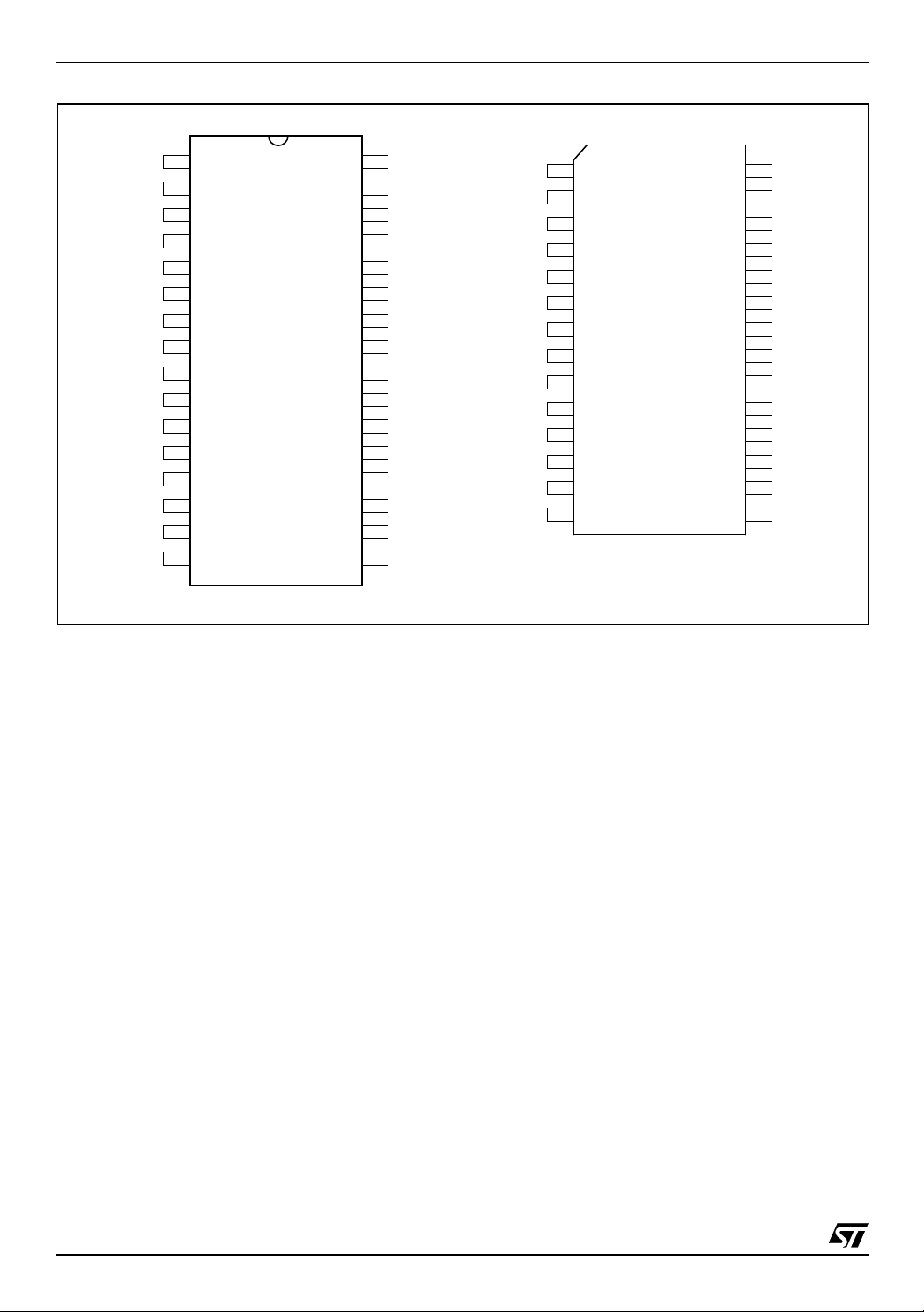
Figure 1.2 ST52F510/F513/F514 SO20/DIP20 Pin Configuration
ST52F510/F513/F514
Vdd
OscOut
OscIn
Vpp
PB0/VREF/AIN0
PB1/AIN1
PB2/AIN2
PB3/AIN3
PB4/AIN4
PB5/AIN5
1
2
3
4
5
6
7
8
9
10
SO20 DIP20
20
19
18
17
16
15
14
13
12
11
Vss
RESET
PA0/SCL
PA1/SDA
PA2/T1OUT
PA3/RX
PA4/TSTRT
PA5/TCLK/TX
PA6/T0OUT
PA7/INT
OscOut
PB0/VREF/AIN0
PB1/AIN1
PB2/AIN2
PB3/AIN3
PB4/AIN4
PB5/AIN5
Figure 1.3 ST52F510/F513/F514 SO16 Pin Configuration
Vdd
OscIn
Vpp
1
2
3
4
5
6
7
8
9
10
20
19
18
17
16
15
14
13
12
11
Vss
RESET
PA0/SCL
PA1/SDA
PA2/T1OUT
PA3/RX
PA4/TSTRT
PA5/TCLK/TX
PA6/T0OUT
PA7/INT
Vdd
OscOut
OscIn
Vpp
PB0/VREF/AIN0
PB1/AIN1
PA7/INT
PA6/T0OUT
1
2
3
4
5
6
7
8
SO16
16
15
14
13
12
11
10
9
Vss
RESET
PA0/SCL
PA1/SDA
PA2/T1OUT
PA3/RX
PA4/TSTRT
PA5/TCLK/TX
11/106
ST52F510/F513/F514
Figure 1.4 ST52F510/F513/F514 SDIP32/DIP28 Pin Configuration
Vdd
VddIO
OscOut
OscIn
Vpp
PB0/VREF/AIN0
PB1/AIN1
PB2/AIN2
PB3/AIN3
PB4/AIN4
PB5/AIN5
PB6/AIN6
PB7AIN7
PC0/SCK
PC1/MOSI
N.C.
1
2
3
4
5
6
7
8
9
10
11
12
13
14
15
16
SDIP32
32
31
30
29
28
27
26
25
24
23
22
21
20
19
18
17
Vss
VssIO
RESET
PA0/SCL
PA1/SDA
PA2/T1OUT
PA3/RX
PA4/TSTRT
PA5/TCLK/TX
PA6/T0OUT
PA7/INT
PC5/TRES
PC4/TX
PC3/SS
PC2MISO
N.C.
Vdd
OscOut
OscIn
Vpp
PB0/VREF/AIN0
PB1/AIN1
PB2/AIN2
PB3/AIN3
PB4/AIN4
PB5/AIN5
PB6/AIN6
PB7/AIN7
PC0/SCK
PC1/MOSI
1
2
3
4
5
6
7
8
9
10
11
12
13
14
SO28
28
27
26
25
24
23
22
21
20
19
18
17
16
15
Vss
RESET
PA0/SCL
PA1/SDA
PA2/T1OUT
PA3/RX
PA4/TSTRT
PA5/TCLK/TX
PA6/T0OUT
PA7/INT
PC5/TRES
PC4/TX
PC3/SS
PC2/MISO
12/106

ST52F510/F513/F514
Table 1.2 ST52F510/F513/F514 SDIP32 Pin List
SDIP32 NAME Programming Phase Working Phase
1 Vdd Digital Power Supply Digital Power Supply
2 VddIO Digital Power Supply Digital I/O Ports Power Supply
3 OSCOUT Oscillator Output
4 OSCIN Oscillator Input
5 Vpp Programming Mode Selector Programming Mode Selector
6 PB0/VREF/AIN0 Digital I/O, A/D Voltage Reference, Analog Input
7 PB1/AIN1 Digital I/O, Analog Input
8 PB2/AIN2 Digital I/O, Analog Input
9 PB3/AIN3 Digital I/O, Analog Input
10 PB4/AIN4 Digital I/O, Analog Input
11 PB5/AIN5 Digital I/O, Analog Input
12 PB6/AIN6 Digital I/O, Analog Input
13 PB7/AIN7 Digital I/O, Analog Input
14 PC0/SCK Digital I/O, SPI Serial Clock
15 PC1/MOSI Digital I/O, SPI Master out Slave in
16 N.C Not Connected
17 N.C Not Connected
18 PC2/MISO Digital I/O, SPI Master in Slave out
19 PC3/SS Digital I/O, SPI Slave Select
20 PC4/TX Digital I/O, SCI Transmission
21 PC5/TRES Digital I/O, Timer/PWM 0 Reset
22 PA7/INT Digital I/O, Non Maskable Interrupt
23 PA6/T0OUT Digital I/O, Timer/PWM 0 output
24 PA5/TCLK/TX Digital I/O, Timer/PWM 0 clock
25 PA4/TSTRT Digital I/O, Timer/PWM 0 start/stop
26 PA3/RX Digital I/O, SCI Reception
27 PA2/T1OUT Digital I/O, Timer/PWM 1 output
28 PA1/SDA Serial Data I/O
29 PA0/SCL Serial Clock
30 RESET General Reset General Reset
Digital I/O, I
Digital I/O, I
2
C Serial Data I/O
2
C Serial Clock
31 VssIO Digital Ground Digital I/O Ports Ground
32 Vss Digital Ground Digital Ground
13/106
ST52F510/F513/F514
Table 1.3 ST52F510/F513/F514 SO28 Pin List
SO28 NAME Programming Phase Working Phase
1 Vdd Digital Power Supply Digital Power Supply
2 OSCOUT Oscillator Output
3 OSCIN Oscillator Input
4 Vpp Programming Mode Selector Programming Mode Selector
5 PB0/VREF/AIN0 Digital I/O, A/D Voltage Reference, Analog Input
6 PB1/AIN1 Digital I/O, Analog Input
7 PB2/AIN2 Digital I/O, Analog Input
8 PB3/AIN3 Digital I/O, Analog Input
9 PB4/AIN4 Digital I/O, Analog Input
10 PB5/AIN5 Digital I/O, Analog Input
11 PB6/AIN6 Digital I/O, Analog Input
12 PB7/AIN7 Digital I/O, Analog Input
13 PC0/SCK Digital I/O, SPI Serial Clock
14 PC1/MOSI Digital I/O, SPI Master out Slave in
15 PC2/MISO Digital I/O, SPI Master in Slave out
16 PC3/SS Digital I/O, SPI Slave Select
17 PC4/TX Digital I/O, SCI Transmission
18 PC5/TRES Digital I/O, Timer/PWM 0 Reset
19 PA7/INT Digital I/O, Non Maskable Interrupt
20 PA6/T0OUT Digital I/O, Timer/PWM 0 output
21 PA5/TCLK/TX Digital I/O, Timer/PWM 0 clock
22 PA4/TSTRT Digital I/O, Timer/PWM 0 start/stop
23 PA3/RX Digital I/O, SCI Reception
24 PA2/T1OUT Digital I/O, Timer/PWM 1 output
25 PA1/SDA Serial Data I/O
26 PA0/SCL Serial Clock
27 RESET General Reset General Reset
28 Vss Digital Ground Digital Ground
Digital I/O, I
Digital I/O, I
2
C Serial Data I/O
2
C Serial Clock
14/106

Table 1.4 ST52F510/F513/F514 SO20/DIP20/SO16 Pin List
ST52F510/F513/F514
SO20
DIP20
SO16 NAME Programming Phase Working Phase
1 1 Vdd Digital Power Supply Digital Power Supply
2 2 OSCOUT Oscillator Output
3 3 OSCIN Oscillator Input
4 4 Vpp Programming Mode Selector Programming Mode Selector
5 5 PB0/VREF/AIN0 Digital I/O, A/D Voltage Reference, Analog Input
6 6 PB1/AIN1 Digital I/O, Analog Input
7 - PB2/AIN2 Digital I/O, Analog Input
8 - PB3/AIN3 Digital I/O, Analog Input
9 - PB4/AIN4 Digital I/O, Analog Input
10 - PB5/AIN5 Digital I/O, Analog Input
11 7 PA7/INT Digital I/O, Non Maskable Interrupt
12 8 PA6/T0OUT Digital I/O, Timer/PWM 0 output
13 9 PA5/TCLK/TX Digital I/O, Timer/PWM 0 clock, SCI transmission
14 10 PA4/TSTRT Digital I/O, Timer/PWM 0 start/stop
15 11 PA3/RX Digital I/O , SCI Re ce ptio n
16 12 PA2/T1OUT Digital I/O, Timer/PWM 1 output
17 13 PA1/SDA Serial Data I/O
18 14 PA0/SCL Serial Clock
19 15 RESET General Reset General Reset
20 16 Vss Digital Ground Digital Ground
Digital I/O, I
Digital I/O, I
2
C Serial Data I/O
2
C Serial Clock
15/106

ST52F510/F513/F514
1.3 Pin Description
ST52F510/F513/F514 pins can be set in digital
input mode, digital output mo de, i nterr upt mode or
in Alternate Functions. Pin configuration is
achieved by mean s of the config uration registe rs.
The functions of the ST52F510/F513/F514 pins
are described below:
V
Main Power Supply Voltage.
DD.
I/O Ports Power Supply Voltage. It is
V
DDIO.
reccomended to connect this pin with a supply
voltage de-coupled with V
in order to improve
DD
the immunity from the n oise generated by th e I/O
switching.
V
. Digital circuit Ground.
SS
. I/O Ports Ground. See V
V
SSIO
DDIO
VPP. Programming/Working mode selector. During
the Programming p hase V
In Working phase V
PP
must be set to VDD.
PP
must be equal to VSS.
OSCin and OSCout. These pins are internally
connected to the on-chip oscillator circuit. A quartz
crystal or a ceramic resonator can be connected
between these two pins in order to allow correct
use of ST52F510/F513/F514 with various stability/
cost trade-offs. An external clock signal can be
applied to OSCin: in this case OSCout must be
grounded. To reduce costs, an RC cir cuit can be
applied to the OSCin pi n to establish the internal
clock frequency, instead of the quartz. Without any
connection, the device can work with its internal
clock generator (10 MHz)
PA0-PA7, PB0-PB7,PC0-PC5. These lines are
organized as I/O ports. Each pin can be configured
as an input, output (with pull- up, pus h-pull, weakpull-up, open-drain, high-impedance), or as an
interrupt source.
VREF, AIN0-AIN7. These pins are used to input
the analog signals into the A/D Converter. An
analog multiplexer is available to switch these
inputs to the A/D Converter. The pin VREF is used
to input an external A/D Reference Voltage.
T0OUT, T1OUT. These pins output the signals
generated by the PWM/Timer 0 and PWM/Timer 1
peripheral.
TRES, TSTRT, TCLK . These pins are related to
the PWM/Timer 0 peripheral and are used for Input
Capture and event counting. The TRES pin is used
to set/reset the Timer; the TSTRT pin is used to
start/stop the counter. The Timer can be driven by
the internal clock or by an external signal
connected to the TCLK pin.
INT. This pin is used as input for the Non-Maskable
(top level) interrupt. The interrupt signal is detected
only if the pin is configured in Alternate Function.
SCL, SDA. These pin are used respectively as
Serial Clock and Serial Data I/O in I
2
C peripheral
protocol. They are used also in Programming
Mode to receive and transmit data.
TX, RX. Serial data output of SCI Transmitter block
(TX) and Serial data input of the SCI Receiver
block (RX).
RESET. This signal is used to reset the ST52F510/
F513/F514 and re-initialize the registers and
control signals. It is also used when switching from
the Programming Mode to Working Mode and vice
versa.
16/106
SCK, MISO, MOSI, SS. These pins are used by
the Serial Peripheral Interface (SPI) peripheral.
SCK is the serial clock line. MISO (Master In Slave
Out) and MOSI (Master Out Slave In) are the serial
data lines, which work in input or in output
depending on if the devic e is working in slave or
master mode. The SS pin allows the selection of
the device master/slave mode.
ST52F510/F513/F514
Control
Signals
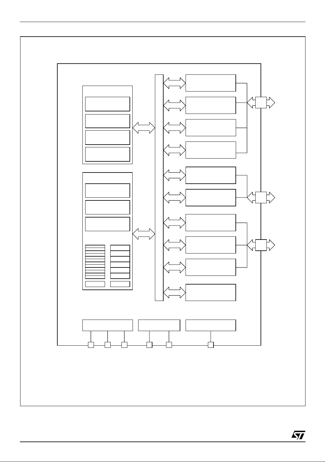
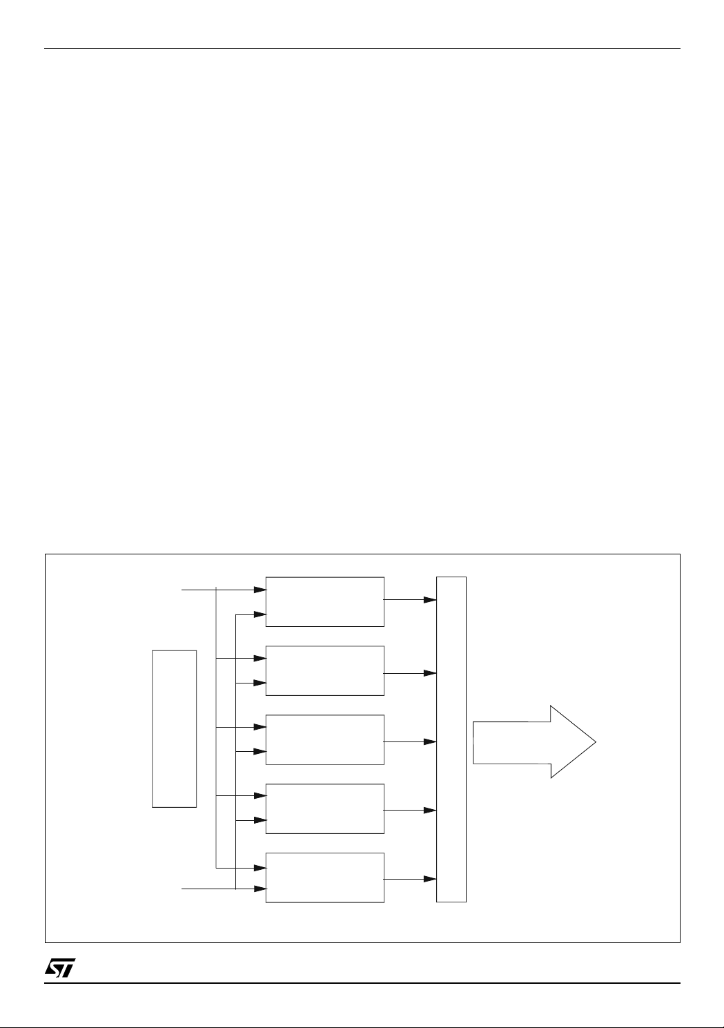
2 INTERNAL ARCHITECTURE
ST52F510/F513/F514’s architecture is Register
File based and is composed of the following blocks
and peripherals:
■ Control Unit (CU)
■ Data Processing Unit (DPU)
■ Decision Processor (DP)
■ ALU
■ Memory Interface
■ up to 256 bytes Register File
■ Program/Data Memory
■ Data EEPROM
■ Interrupts Controller
■ Clock Oscillator
■ PLVD and POR
■ Digital I/O ports
■ Analog Multiplexer and A/D Converter
■ Timer/PWMs
2
■ I
C
■ SPI
■ SCI
Figure 2.1 CU Block Diagram
2.1 Control Unit and Data Processing Unit
The Control Unit (CU) decodes the instructions
stored in the Program Mem ory and gene rates the
appropriate control s ignals. The main parts of the
CU are illustrated in Figure 2.1.
The five different parts of the CU manage Loading,
Logic/Arithmetic, Jump, Control and the Fuzzy
instruction set.
The block called “ Collector” manages the sig nals
deriving from the different parts of the CU. The
collector defines the signals for the Data
Processing Unit (DPU) and Decision Processor
(DP), as well as for th e different peripherals of the
ICU.
The block called “Arbiter” manages the different
parts of the CU, so that only one part of the system
is activated during working mode.
The CU structure is extremely flexible and was
designed with the purp ose of easily adapting the
core of the microcontroller to market need s. New
instruction sets or new pe ripherals can easil y be
included without changing the structure of the
microcontroller, maintaining code compatibility.
A set of 107 different instructions is available. Each
instruction requires a number of clock pulses to be
performed that depe nds on the complexity of the
instruction it self. The clock pulses t o execute the
instructions are driv en dir ec tly by the ma sterclock,
which has the same frequency of the oscillator
signal supplied.
MicroCode
A
R
B
I
T
E
R
Clock Master
Loading
Instruction Set
Logic Arithmetic
Instruction Set
Jump
Instruction Set
Control
Instruction Set
Decision Processor
Instruction Set
C
O
L
L
E
C
T
O
R
17/106

ST52F510/F513/F514
Figure 2.2 Data Processing Unit (DPU)
Interrupts Unit
Program Memory
Input Registers
Peripherals
REGISTER FILE
ADDRESS
PROGRAM COUNTER
REGISTER
FILE
256 Bytes
ACCUMULATOR
FLAGS REG.
DECISION
PROCESSOR
REGISTERS
ALU
Memory Address
Control Unit
Peripherals
The DPU receives, stores and sends the
instructions deriving from the Program/Data
Memory, Register File or from the peripherals. It is
controlled by the CU on the basis of the dec oded
instruction. The Fuzzy registers store the partial
results of the f uz zy c om puta tion. The accumul ator
register is used by the ALU and i s not accessible
directly: the instructions used by the ALU can
address all the Register File locations as
operands, allowing a more compact code and a
faster execution.
The following addressing modes are available:
inherent, immediate, direct, indirect, bit direct.
2.1.1 Program Counter.
The Program Counter (PC) is a 16-bit register that
contains the addre ss of the next memory location
to be processed by the core. This memory location
may be both an instruction or data address.
The Program Counter’s 16-bit length allows the
direct addressing of a maximum of 64 Kbytes in the
Program/Data Memory space.
18/106
The PC can be changed in the following ways:
■ JP (Jump) PC = Jump Address
■ Interrupt PC = Interrupt Vector
■ RETI PC = Pop (stack)
■ RET PC = Pop (stack)
■ CALL PC = Subroutines address
■ Reset PC = Reset Vector
■ Normal Instruction PC = PC + 1
2.1.2 Flags.
The ST FIVE core includes differen t sets of flags
that correspond to 2 different modes: normal mode
and interrupt mode. Each set of fla gs consist of a
CARRY flag (C), ZERO flag (Z) and SIGN flag (S).
Each set is stacked: one set of flags is used during
normal operation and oth er sets are used during
each level of interrupt. Formally, the user has to
manage only one set of flags: C, Z and S since the
flag stack operation is performed automatically.

ST52F510/F513/F514
Each interrupt leve l ha s i t s own set of flags, which
is saved in the Flag Stack during interrupt
servicing. These flags are restored from the Flag
Stack automatically when a RETI instruction is
executed.
If the ICU was in normal mode before an interrupt,
after the RETI instruction is executed, the normal
flags are restored.
Note: A subroutine CALL is a normal mode
execution. For this reason a RET instruction,
consequent to a CALL instruction, doesn’t affect
the normal mode set of flags.
Flags are not cleared during context switching and
remain in the state they were in at the exit of the
last interrupt routine switching.
The Carry flag is set when an overflow occurs
during arithmetic operations, otherwise it is
cleared. The Sign flag is set when an underflow
occurs during arithmetic operations, otherwise it is
cleared.
The flags, related to the current context, can be
checked by reading the FLAGS Input Register 38
(026h).
2.2 Arithmetic Logic Unit
The 8-bit Arithmetic Logic Unit (ALU) performs
arithmetic calcu lations and l ogic instructi ons such
as: sum, subtraction , bitwise AND, OR, XOR, bit
set and reset, bit test and branch, right/left shift and
rotate (see the Chapter 9 Instruction Set for further
details).
In addition, the ALU of ST52F510/F513/F514 can
perform multiplicati on (MULT) and division (DIV).
Multiplication is performed by using 8 bit operands
storing the result in 2 registers (16 bi t values); the
division instruction addresses the MSB of the
dividend (the LSB is stored in the next addres s):
the result and remainder are stored in these source
addresses (see Figure 2.3 and Figure 2.4).
In order to manage s igned type values, the ALU
also performs additio n and subtraction with offset
(ADDO and SUBO). These instructions
respectively subtract and add 128 to the overall
result, in order to ma nage values logically in the
range between -128,127.
Figure 2.3 Multiplication
RAM
000h
001h
002h
i
j-1
j
j+1
0FDh
0FEh
0FFh
REG. j REG. i
LSB
X
16 Bit
MSB
Figure 2.4 Division
REG. j REG. j+1
RAM
000h
001h
002h
i-1
i
i+1
j-1
j
j+1
0FDh
0FEh
0FFh
:
REMAINDER QUOTIENT
REG. i
19/106

ST52F510/F513/F514
2.3 Register Description
Flags Register (FLAG)
Input Register 38 (026h) Read Only
Reset Value: 0000 0000 (00h)
70
-----ZSC
Bit 7-3: Not Used
Bit 2: Z Zero flag
Bit 1: S Sign flag
Bit 0: C Carry flag
20/106

ST52F510/F513/F514
3 ADDRESSING SPACES
ST52F510/F513/F514 has six separate
addressing spaces:
■ Register File
■ Program/Data Memory
■ Stacks
■ In put Regi st er s
■ Output Registers
■ Configuration Registers
Each space is addressed by a load type instruction
that indicates the source and the destination space
in the mnemonic code (see Figure 3.1).
3.1 Memory Interface
The read/write operation in the s pace addresses
are managed by the Memo ry Inter face , whic h ca n
recognize the ty pe of memor y addressed a nd set
the appropriate access time and mode.
In addition, the Memory Interface manages the In
Application Program ming (IAP) functions in Flash
devices like writing cycle and memory write
protection.
Figure 3.1 Addressing Spaces
3.2 Register File
The Register File con sist s o f 2 56 g ene ra l p urpos e
8-bit RAM locations called “registers” in order to
recall the functionality.
The Register File exchanges data with all the other
addressing spaces and is used by the ALU to
perform all the arithmetic and logic instructions.
These instructions have any Register File address
as operands.
Data can be moved from one location to another by
using the LDRR inst ruction; see further ahead for
information on the instr uction used to move data
between the Register File and the other
addressing spaces.
3.3 Program/Data Memory
The Program/Data Memory con sists of both nonvolatile memory (Flash, EEPROM) and RAM
memory benches.
Non-volatil e memory (NV M) is mainly us ed to store
the user program and can al so be used to store
permanent data (constant, look-up tables).
Each RAM bench consists of 256 locations used to
store run-time user data. At least one bench is
present in the devices. RAM benches are also
used to implement both System and User Stacks .
PROGRAM/DATA MEMORY
NON VOLATILE MEMORY
RAM BANKS
AND STACKS
LDCE
LDPE
LDER
LDRE
STFive CORE
REGISTER FI LE
INPUT REGISTERS
LDFR
LDRI
LDCNF
GETPG
DECISION
PROCESSOR
REGISTERS
PGSETR
PROGRAM
COUNTER
CU
DPU
ALU
LDPR
LDCR
ON CHIP PERIPHERALS
OUTPUT
REGISTERS
PERIPHERAL
CONFIGURATION
REGISTERS
PERIPHERAL
PERIPHERAL
BLOCK
BLOCK
BLOCK
21/106
ST52F510/F513/F514
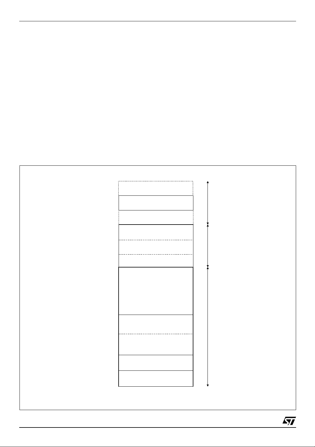
NVM is always located beginning after the first
locations of the addressing space. RAM banks are
always located after NVM.
NVM is organized in acco rdance to the following
blocks (see Figure 3.2):
■
Reset Vector block
(from address 0 to 2)
contains an absolute jump instruction to the first
user program instruction. The Assembler tool
automatically fills these locations with correct
data.
■
Interrupt Vectors block
(from location 3 up to
32) contains the interrupt vectors. Each address
is composed of three bytes (the jump opcode
and the 16 bit address). Interrupt vectors are set
by using IRQ pseudo-instruction (see the
Programming Manual).
Figure 3.2 Program/Data Memory Organization
FFFFh
~~
307Fh
OPTION BYTES
3000h
~~
20FFh
SYSTEM STACK
■
Mbfs Setting block
(just after the interrupt
vectors) contains the coordinates of the vertexes
of every Mbf defined in the program. The last
address that can be assigned to this block is
1023. This area is dynamically assigned
according to the size of the fuzzy routines. The
memory area that remains unused, if any, is
assigned to the Program Instructions block.
■
The Program Instructions block
(just after the
last Mbf data through the last NVM address)
contains the instruction of the user program and
the permanent data.
■
Option bytes block
(from location 3000h to
307Fh) is the addressing space reserved for the
option bytes. In ST 52F510/F513/F514, o nly the
location from 3000h to 3007h are used.
SPACE NOT
ADDRESSABLE
2000h
0400h
0021h
0003h
0000h
DATA
USER STACK
PROGRAM INSTRUCTIONS
AND PERMANENT DATA
PROGRAM INSTRUCTIONS
AND PERMANENT DATA
MEMBERSHIP FUNCTIONS
PARAMETERS
INTERRUPT VECTORS
RESET VECTOR
RAM
BENCH
NON
VOLATILE
MEMORY
22/106
ST52F510/F513/F514
Flash and EEPROM are pr ogrammed electrically
just applying the supply voltage (2.7 V to 5.5 V) and
it is also erased electrically; this feature allows the
user to easily reprogram the memory without
taking the device off from the board (In Situ
Programming ISP). Data and commands are
transmitted through t he I
2
C serial communicatio n
protocol. Data can also be written run-time with the
In Application Programming (IAP)
NVM can be locked by the user during the
programming phase, in orde r to prevent external
operation such as rea ding the program code an d
assuring protection of user intellectual property.
Flash and EEPROM pages can be protected by
unintentional writings.
The operations that can be performed on the NVM
during the Programmin g Phase, ISP and IAP ar e
described in detail in the Section 4.
Figure 3.3 System and User Stack
RAM BENCH
20FFh
20FEh
SYSTEM STACK
POINTER
SYSTEM STACK
LEVEL 1
SYSTEM STACK
LEVEL 2
SYSTEM STACK
LEVEL 3
SYSTEM STACK
LEVEL 4
IRQ
3.4 System and User Stacks
The System and User Stacks are located in the
Program/Data memory in the RAM benches.
System Stacks are used to push the Program
Counter (PC) after an Interrupt Request or a
Subroutine Call. After a RET (Return from a
subroutine) or a RETI (Return from an interrupt)
the PC that is saved is popped from the stack and
restored. After an inter rupt request, the flags are
also saved in a r eserved s tack insi de the cor e, so
each interrupt has its own flags.
The System Stack is located in the last RAM bench
starting from the last address (255) inside the
bench page. The System Stack Pointer (SSP) can
be read and modified by the user. For each level of
stack 2 bytes of the RAM are used. The SSP points
to the first currently available stack position. When
a subroutine call or interrupt request occurs, the
content of the PC is stored in a couple of locations
pointed to by the SSP that is decreased by 2.
PROGRAM COUNTE R
RETI
LOCATION ADRESS
PAGE NUMBER
REGISTER FILE
LSB
MSB
USER STACK
POINTER
2001h
2000h
USER DATA
USER STACK LEVEL 4
USER STACK LEVEL 3
USER STACK LEVEL 2
USER STACK LEVEL 1
PUSH X
POP X
REGISTER X
CONFIGURATION REGISTERS
USER STACK TOP LSB
USER STACK TOP MSB
23/106

ST52F510/F513/F514
When a return occurs (R ET or RETI instruction),
the SSP is increas ed by 2 and the data stored in
the pointed locations co uple is restored back into
the PC.
The current SSP can be read and write in the
couple of Configuration Reg isters 44 02Ch (MSB :
page number, always 32 020h) and 45 02Dh (LSB:
location address) ( see Figure 3.3). In ST52F51 0/
F513/F514 the user can only consider the LSB
because the MSB is always the same.
The User Stack is used to s tore user data and is
located beginning fr om a RAM bench locati on set
by the user (USTP) by writing the couple of
Configuration Registers 5 005h (MSB: page
number) and 6 005h (LSB: location address) (see
Figure 3.3). Register 5, which is the page number,
must always be set to a va lue between 32 (020h)
and 255 (0FFh): values higher than 32 always
address RAM on page 32.
Note: In ST52F510/F513/F514 MSB doesn’t have
to be set or read because the RAM is only 256
bytes. The LSB of the user stack is equal to 0 at
reset. The LSB of the system stack is equal to 255
at reset.
This feature allows a flexible use of the User Stack
in terms of dimensi on and to avoid ove rlaps. The
User Stack Pointer (USP) points to the first
currently availab le stack location. When the user
stores a byte value contain ed in the Register File
by using the PUSH in structi on, the valu e is store d
in the position pointed to by the USP that is
increased (the User Stack o rder is oppo site to the
System Stack one). Wh en the user takes a valu e
from the User Stack with the POP inst ruction, the
USP is decreased and the value pointed to is
copied in the specified Register File location.
By writing the USTP, the new address is
automatically written in the USP. The current USP
can be read from the Input Registers 11 0Bh
(MSB: page number, always 32 020h) and 12 0Ch
(LSB: location address) (see Figure 3.3). In
ST52F510/F513/F514 the user can only consider
the LSB because the MSB is always the same.
Note: The user must pay close attention to avoid
overlapping user and Stacks data. The User Stack
Top location and the System Stack Pointer should
be configured with c are in order to have enough
space between the two stacks.
3.5 Input Registers
The ST52F510/F513/F514 Input Regis ters bench
consists of a file of 8-bit regis ters containing data
or the status of the p eripherals. For exam ple, the
Input Registers contain data converted by the
ADC, Ports, serial communication peripherals,
Timers, etc.
The Input Registers can be accessed by using the
LDRI instruction that loads the specified Register
File address with the contents of the specified
Input Register. See the Programming Manual for
further details on this instruction. The Input
Registers are read-only registers.
In order to simplify the concept, a mnemonic name
is assigned to each register. The same name is
used in Visual FIVE devel opmen t tools. The list of
the Input Registers is shown in Table 3.1.
3.6 Output registers
The ST52F510/F513/F514 Output Registers
bench consists of a file of 8-bit registers containing
data sent to the Periphe rals and the I/O Port s (for
example: Timer Counter s, data to be transmitted
by the serial communication peripherals, data to be
sent to the Port pins in output, etc.).
The registers are located inside the Peripherals
and Ports, which allow flex ibility and modul arity in
the design of new family devices.
The Output Registers are write only. In order to
access the configuration Register the user can use
the following instructions:
■ LDPI: loads the immediate value in the specified
Output Register.
■ LDPR: loads the contents of the specified
Register File location into the output register
specified. This instruction allows computed data
to be sent to Peripherals and Ports.
■ LDPE direct: loads th e c ont ents of the sp ec ifi ed
Program/Data Memory l ocation into the output
register specified. This instruction allows data to
be sent to Peripherals and Ports from a table.
■ LDPE indirect: loads the contents of the
Program/Data Memo ry location whose address
is contained in the specified Register File
location into the output reg ister specified. This
instruction allows da ta to be se nt to Per ipheral s
and Ports from a table pointed to by a register.
See the Programming manual for further details
about these instructions.
In order to simplify the concept, a mnemonic name
is assigned to each register. The same name is
used in Visual FIVE devel opmen t tools. The list of
the Output Registers is shown in Table 3.2.
24/106

ST52F510/F513/F514
3.7 Configuration Registers & Option Bytes
The ST52F510/F513/F514 Configuration
Registers bench con si st s o f a f il e of 8- bit r egi ste rs
that allows the configuration of all the ICU blocks.
The registers are located inside the block they
configure in order to ob tain greater flexibility and
modularity in the design of new f amily devices. In
the Configuration Registers, each bit has a
peculiar use, so the logic level of each of them
must be considered.
Some special c onfig urati on dat a, that needs to b e
load at the start-up and not further changed, are
stored in Option Bytes. These are loaded only
during the device program ming phase. See Tabl e
3.3 and Section 4 for a d etailed descr iption of the
Option Bytes.
The Configuration Registers are readable and
writable; the address es refer to the sam e register
both in read and in writ e. In order to access the
Configuration Register the user can work in
several modes by utilizing the following
instructions:
■ LDCI: loads the immediate value in the
Configuration Register specified and is the most
commonly used to write configuration data.
■ LDCR: loads the Configuration Register
specified with the contents of the specified
Register File location, allowing a parametric
configuration.
■ LDCE: loads the Configuration Register
specified with the contents of the specified
Program/Data Memory location, allowing the
configuration data to be taken from a table.
■ LDCNF: loads the Register File location
specified with the c ontents of the Con figuration
Register indicated, allowing for the inspection of
the configuration of the device (permitting s afe
run-time modifications).
In order to simplify the concept, a mnemonic name
is assigned to each register. The same name is
used in Visual FIVE devel opmen t tools. The list of
the Configuration Registers is shown in Table 3.4.
25/106

ST52F510/F513/F514
Table 3.1 Input Registers
Mnemonic Description Address
PORT_A_IN Port A data Input Register 0 00h
PORT_B_IN Port B data Input Register 1 01h
PORT_C_IN Port C data Input Register 2 02h
- Not Used 3 03h
- Not Used 4 04h
SPI_IN Serial Peripheral Interface data Input Register 5 05h
I2C_IN
I2C_SR1
I2C_SR2
2
C Interface data Input Register
I
2
I
C Interface Status Register 1
2
I
C Interface Status Register 2
606h
707h
808h
- Not Used 9 09h
- Not Used 10 0Ah
USP_H User Stack Pointer (MSB) 11 0Bh
USP_L User Stack Pointer (LSB) 12 0Ch
- Not Used 13-2 0
0Dh-
014h
PWM0_COUNT_IN_H PWM/Timer 0 Counter Input Register (MSB) 21 015h
PWM0_COUNT_IN_L PWM/Timer 0 Counter Input Register (LSB) 22 016h
PWM0_STATUS PWM/Timer 0 Status Register 23 017h
PWM0_CAPTURE_H PWM/Timer 0 Capture Register (MSB) 24 018h
PWM0_CAPTURE_L PWM/Timer 0 Capture Register (LSB) 25 019h
PWM1_COUNT_IN_H PWM/Timer 1 Counter Input Register (MSB) 26 01Ah
PWM1_COUNT_IN_L PWM/Timer 1 Counter Input Register (LSB) 27 01Bh
PWM1_STATUS PWM/Timer 1 Status Register 28 01Ch
PWM1_CAPTURE_H PWM/Timer 1 Capture Register (MSB) 29 01Dh
PWM1_CAPTURE_L PWM/Timer 1 Capture Register (LSB) 30 01Eh
- Not Used 31-3 5
SCI_IN Serial Communication Interface RX data Input Register 36 024h
SCI_STATUS Serial Communication Interface Status Register 37 025h
FLAGS Flag Register 38 026h
AD_OVF 10-bit A/D Converter Overflow Register 39 027h
IAP_SR In Application Programming Status Register 40 028h
26/106
01Fh-
023h

ST52F510/F513/F514
Table 3.1 Input Registers
Mnemonic Description Address
CHAN0_H 10-bit A/D Converter Channel 0 data Input Register (MSB) 41 029h
CHAN0_L 10-bit A/D Converter Channel 0 data Input Register (LSB) 42 02Ah
CHAN1_H 10-bit A/D Converter Channel 1 data Input Register (MSB) 43 02Bh
CHAN1_L 10-bit A/D Converter Channel 1 data Input Register (LSB) 44 02Ch
CHAN2_H 10-bit A/D Converter Channel 2 data Input Register (MSB) 45 02Dh
CHAN2_L 10-bit A/D Converter Channel 2 data Input Register (LSB) 46 02Eh
CHAN3_H 10-bit A/D Converter Channel 3 data Input Register (MSB) 47 02Fh
CHAN3_L 10-bit A/D Converter Channel 3 data Input Register (LSB) 48 030h
CHAN4_H 10-bit A/D Converter Channel 4 data Input Register (MSB) 49 031h
CHAN4_L 10-bit A/D Converter Channel 4 data Input Register (LSB) 50 032h
CHAN5_H 10-bit A/D Converter Channel 5 data Input Register (MSB) 51 033h
CHAN5_L 10-bit A/D Converter Channel 5 data Input Register (LSB) 52 034h
CHAN6_H 10-bit A/D Converter Channel 6 data Input Register (MSB) 53 035h
CHAN6_L 10-bit A/D Converter Channel 6 data Input Register (LSB) 54 036h
CHAN7_H 10-bit A/D Converter Channel 7 data Input Register (MSB) 55 037h
CHAN7_L 10-bit A/D Converter Channel 7 data Input Register (LSB) 56 038h
27/106

ST52F510/F513/F514
Table 3.2 Output Registers
Mnemonic Description Address
PORT_A_OUT Port A data Output Register 0 00h
PORT_B_OUT Port B data Output Register 1 01h
PORT_C_OUT Port C data Output Register 2 02h
- Not Used 3 03h
- Not Used 4 04h
SPI_OUT Serial Peripher al Inte rfa ce data Outp ut Regis te r 5 05h
I2C_OUT
PWM0_COUNT_OUT_H PWM/Timer 0 Counter Output Register (MSB) 7 07h
PWM0_COUNT_OUT_L PWM/Timer 0 Counter Output Register (LSB) 8 08h
PWM0_RELOAD_H PWM/Timer 0 Reload Register (MSB) 9 09h
PWM0_RELOAD_L PWM/Timer 0 Reload Register (LSB) 10 0Ah
PWM1_COUNT_OUT_H PWM/Timer 1 Counter Output Register (MSB) 11 0Bh
PWM1_COUNT_OUT_L PWM/Timer 1 Counter Output Register (LSB) 12 0Ch
PWM1_RELOAD_H PWM/Timer 1 Reload Register (MSB) 13 0Dh
PWM1_RELOAD_L PWM/Timer 1 Reload Register (LSB) 14 0Eh
SCI_OUT Serial Communication Interface TX data Output Register 23 017h
2
C Interface data Output Register
I
606h
Table 3.3 Option Bytes
Mnemonic Description Address
OSC_CR Oscillator Control Register 0 00h
CLK_SET Clock Parameters 1 01h
OSC_SET Oscillator Set-Up 2 02h
PLDV_CR Programmable Low Voltage Detector Control Register 3 03h
WDT_EN HW/SW Watchdog selector 4 04h
PG_LOCK First Page Write Protected 5 05h
PG_UNLOCK First Page not Write Protected 6 06h
WAKEUP Wake Up from Halt Time 7 07h
28/106
ST52F510/F513/F514
Table 3.4 Configuration Registers
Mnemonic Description Address
INT_MASK Interrupt Mask Register 0 00h
INT_POL Interrupts Polarity 1 01h
INT_PRL_H Interrupt Priority Reg ist er (hig he r priority ) 2 02h
INT_PRL_M In te rru pt Pri orit y Regist er (me di um prior ity) 3 03h
INT_PRL_L Interrupt Priority Register (lower prior ity) 4 04h
USTP_H User Stack Top Pointer (MSB) 5 05h
USTP_L User Stack Top Pointer (LSB) 6 06h
WDT_CR Watchdog Configurati on Re gis te r 7 07h
AD_CR1 10-bit A/D Converter Control Register 1 8 08h
PWM0_CR1 PWM/Timer 0 Configuration Register 1 9 09h
PWM0_CR2 PWM/Timer 0 Configuration Register 2 10 0Ah
PWM0_CR3 PWM/Timer 0 Configuration Register 3 11 0Bh
PWM1_CR1 PWM/Timer 1 Configuration Register 1 12 0Ch
PWM1_CR2 PWM/Timer 1 Configuration Register 2 13 0Dh
- Not Used 14 0Eh
- Not Used 15 0Fh
I2C_CR
I2C_CCR
I2C_OAR1
I2C_OAR2
2
I
C Interface Control Register
2
I
C Interface Clock Control Register
2
I
C Interface Own Address Register 1
2
I
C Interface Own Address Register 2
16 010h
17 011h
18 012h
19 013h
SPI_CR Serial Peripheral Inte rfa ce Con trol Regi ste r 20 014h
SPI_STATUS_CR Serial Peripheral Inte rfa ce Con trol-Status Register 21 015h
SCI_CR1 Serial Communication Interface Control Register 1 22 016h
SCI_CR2 Serial Communication Interface Control Register 2 23 017h
PORT_A_PULLUP Port A Pull Up enable/disable Register 24 018h
PORT_A_OR Port A Option Register 25 019h
29/106
ST52F510/F513/F514
Table 3.4 Configuration Registers
Mnemonic Description Address
PORT_A_DDR Port A Data Direction Register 26 01Ah
PORT_A_AF Port A Alternate Function selection Register 27 01Bh
PORT_B_PULLUP Port B Pull Up enable/disable Register 28 01Ch
PORT_B_OR Port B Option Register 29 01Dh
PORT_B_DDR Port B Data Direction Register 30 01Eh
PORT_B_AF Port B Alternate Function selection Register 31 01Fh
PORT_C_PULLUP Port C Pull Up enable/disable Register 32 020h
PORT_C_OR Port C Option Register 33 021h
PORT_C_DDR Port C Data Direction Register 34 022h
PORT_C_AF Port C Alternate Function selection Register 35 023h
- Not Used 36-4 2
SCI_CR3 Serial Communication Interface Control Register 3 43 02Bh
SSP_H System Stack Pointer (MSB) 44 02Ch
SSP_L System Stack Pointer (LSB) 45 02Dh
CPU_CLK CPU Clock Prescaler 46 02Eh
AD_CR2 10-bit A/D Converter Control Register 2 47 02Fh
024h-
02Ah
30/106
 Loading...