


®
ST52T400/T440/E440
8-BIT INTELLIGENT CONTROLLER UNIT (ICU)
Timer/PWM, Analog Comparator, Triac/PWM Timer, WDG
Memories
■ Upto8KbytesEPROM/OTP
■ 128/256 bytes of RAM
■ Readout Protection
Core
■ Register File Based Architecture
■ 55 instructions
■ Hardware multiplication and division
■ Decision Processor for the implementation of
Fuzzy Logic algorithms
Clock and Power Supply
■ Up to 20 M H z clock frequency.
■ On-c hip Power On Reset (POR) andBrown Out
Detector (BOD)
■ P ower Saving features
ST52T400/T440/E440/T441
PRELIMINARY DATASHEET
Interrupts
■ 6 interrupt vectors
■ Top Level External Interrupt (INT)
I/O Ports
■ 13 or 21 I /O PINs configurable in Input and
Output mode
■ High current sink/source in all pins. Triac Driver
output can supply 50 mA
Peripherals
■ Programmable 8-bit Timer/PWMs wi th internal
16-bit Prescaler featuring:
– PWM outp ut
– Input capture
– Output compare
– Pulse generator mode
■ Watchdog timer
■ 6-channels Analog Comparator with 16-bit
Timer (not available in ST52T400)
■ Triac/PWM Driver Timer with zero crossing
detector and high current capability for:
– PWM mode
–BurstMode
– Phase Angle Partialization mode
Development tools
■ High level Software to ols
■ Emulator
■ Low cost Programmer
■ Gang Programmer
Rev. 2.9 - November 2002 1/94
This ispreliminary information on a new product now in development or undergoing evaluation. Details are subject to change without notice.
ST52T400/T440/E440/T441
ST52T400/T440/E440/T441 Type List
ST52 Device
ST52T400Fmpy 1/2/4/8K 128/256
ST52T400Gmpy 1/2/4/8K 128/256 21
ST52T440Fmpy 1/2/4/8K 128/256
ST52T440Gmpy 1/2/4/8K 128/256
ST52E440F3D6 8K 256 13 CDIP20W
ST52E440G3D6 8K 256 21 CDIP28W
ST52T441Fmpy 1/2/4/8K 128/256
ST52T441Gmpy 1/2/4/8K 128/256
ST52E441F3D6 8K 256 13 CDIP20W
ST52E441G3D6 8K 256 21 CDIP28W
Note: devices with 1-2K NVM have 128 RAM; devices with 4-8K NVM have 256 RAM
NVM
(bytes)
RAM
(bytes)
TIMER/
PWM
1No 1YesYes
1
1
Analog
Comparator
4ch
6ch
4ch
6ch
Triac
Driver/
PWM
1YesYes
1YesYesNo
WDT
POR,
Pull up I/Os Package
BOD
Yes
13
13
21
13
21
SO20,
PDIP20
SO28,
PDIP28
SO20,
PDIP20
SO28,
PDIP28
SO20,
PDIP20
SO28,
PDIP28
COMMON FEATURES ST52T400 ST52x440/ST52x441
Temperature Range -40 to + 85 °C -40 to + 85 °C
Operating Supply 2.7 to 5.5 V 4.5 to 5.5 V
CPU Frequency Up to 20 MHz Up to 20 MHz
Legend:
Sales code: ST52tnnncmpy
Memory type (t): F=FLASH, T=OTP, E=EPROM
Subfamily (nnn): 400, 410, 420, 430, 440, 441
Pin Count (c): Y=16 pins, F=20 pins, G=28 pins, K=32/34 pins, J=42/44 pins
Memory Size (m): 0=1 Kb, 1=2 Kb, 2=4 Kb, 3=8 Kb
Packages (p): B=PDIP, D=CDIP, M=PSO, T=TQFP
Temperature (y): 0=+25, 1=0 +70, 3=-40 +125, 5=-10 +85, 6=-40 +85, 7=-40 +105
2/94

TABLE OF CONTENTS
ST52T400/T440/E440/T441
TABLE OF CONTENTS
1GENERALDESCRIPTION......................................... 7
1.1Introduction...................................................................7
1.2 Operational Description .........................................................8
1.2.1MemoryProgrammingPhase................................................ 8
1.2.2WorkingMode............................................................ 8
1.3 PinDescription...............................................................18
2INTERNALARCHITECTURE...................................... 19
2.1ControlUnitandDataProcessingUnit.............................................19
2.1.1ProgramCounter ........................................................ 19
2.1.2Flags.................................................................. 21
2.2AddressSpaces..............................................................21
2.2.1RamandStack.......................................................... 22
2.2.2 Input Registers Bench . . . ................................................. 22
2.2.3ConfigurationRegisters ................................................... 23
2.2.4OutputRegisters......................................................... 23
2.3FuzzyComputation............................................................25
2.3.1FuzzyInference ......................................................... 25
2.3.2FuzzyficationPhase...................................................... 25
2.3.3InferencePhase......................................................... 26
2.3.4Defuzzyfication.......................................................... 26
2.3.5 Input Membership Function ................................................ 27
2.3.6OutputSingleton......................................................... 27
2.3.7FuzzyRules............................................................ 27
2.4 Arithmetic Logic Unit. . . ........................................................30
2.4.1 Address ing Modes ....................................................... 30
2.4.2InstructionTypes ........................................................ 30
3EPROMProgramming........................................... 33
3.1EPROMProgrammingPhaseProcedure...........................................34
3.1.1EPROMOperation....................................................... 35
3.1.2EPROMLocking......................................................... 35
3.1.3EPROMWriting ......................................................... 35
3.1.4EPROMReading/VerifyMarginMode........................................ 35
3.1.5StandbyMode.......................................................... 36
3.1.6IDcode................................................................ 36
3.2EpromErasure...............................................................36
4INTERRUPTS.................................................. 37
4.1InterruptOperation............................................................37
4.2 Global Interrupt Request Enabling ................................................38
4.3InterruptSources .............................................................38
4.4 Interrupt Maskability . . . ........................................................38
3/94

ST52T400/T440/E440/T441
4.5InterruptPriority ..............................................................40
4.6InterruptsandLowpowermode..................................................41
4.7InterruptRESET..............................................................41
5CLOCK,RESET&POWERSAVINGMODE.......................... 42
5.1ClockSystem................................................................42
5.2Reset.......................................................................43
5.2.1ExternalReset .......................................................... 43
5.2.2ResetOperation......................................................... 43
5.2.3Power-onReset(POR).................................................... 43
5.2.4Brown-OutDetector(BOD)................................................. 44
5.3PowerSavingModes..........................................................44
5.3.1WaitMode.............................................................. 44
5.3.2HaltMode.............................................................. 44
6I/OPORTS.................................................... 46
6.1Introduction..................................................................46
6.2 Input Mode ..................................................................47
6.3OutputMode.................................................................47
6.4AlternateFunctions............................................................48
6.5I/OPortConfigurationRegisters..................................................48
7 ANALOG COMPARATOR (ST52x440/441)........................... 50
7.1AnalogModuleOverview.......................................................50
7.2ComparatorMode.............................................................50
7.3A/DConverterMode...........................................................50
7.3.1OperatingModes........................................................ 51
8WATCHDOGTIMER............................................. 54
8.1 Functional Desc ript ion . ........................................................54
8.2RegisterDescription...........................................................55
9PWM/TIMER................................................... 56
9.1TimerMode..................................................................56
9.2PWMMode..................................................................57
9.3TimerInterrupt ...............................................................59
10TRIAC/PWMDRIVER........................................... 63
10.1TRIAC/PWMDriverSetting.....................................................64
10.2PWMModeSettings..........................................................65
10.3BurstMode.................................................................66
10.4PhaseAnglePartializationWorkingMode.........................................68
11ELECTRICALCHARACTERISTICS............................... 72
11.1ParameterConditions.........................................................72
11.1.1MinimumandMaximumvalues ............................................ 72
11.1.2Typicalvalues.......................................................... 72
11.1.3Typicalcurves.......................................................... 72
11.1.4 Loading c apac it or ....................................................... 72
11.1.5Pininputvoltage........................................................ 72
11.2AbsoluteMaximumRatings ....................................................72
4/94

ST52T400/T440/E440/T441
TABLE OF CONTENTS
11.3 Recommended Operating Condition. . . ...........................................74
11.4SupplyCurrentCharacteristics..................................................75
11.5Brown-OutDetectorcharacteristics ..............................................76
11.6ClockandTimingCharacteristics................................................77
11.7MemoryCharacteristics .......................................................78
11.8ESDPinProtectionStrategy....................................................79
11.8.1 Standard Pi n Protection . ................................................. 79
11.9PortPinCharacteristics .......................................................80
11.9.1 General Charact eristics . ................................................. 80
11.10..........................................................................82
11.11ControlPinCharacteristics ....................................................84
11.11.1RESET pin ........................................................... 84
11.11.2Poweronreset........................................................ 84
11.11.3VPPpin.............................................................. 84
11.12AnalogComparatorCharacteristics.............................................85
11.13TriacDriverCharacteristics....................................................85
ORDERINGINFORMATION........................................ 92
5/94

ST52T400/T440/E440/T441
6/94

ST52T400/T440/E440/T441
1 GENERAL DESCRIPTION
1.1 Introduction
ST52x400/440/441 are 8-bit Intelligent Control
Units (ICU) of th e ST Five Family, w hich are able
to perform both boolean and fuz z y al gorithms in
an efficient manner, in order to reac h the best performances that the two methodologies allow.
ST52x400/440/441 is produced by STM icroelectronics using the reliable high performa nce CMOS
process, including integrated-on-chip peripherals
that allow maximization of system reliability,
decreasing system costs and minimizing the
number of externa l components.
The flexible I/O configuration of ST52x400/440/
441 allows for an interface with a wide range of
external devices, like D /A converters or power
control devices.
ST52x400/440/441 pins are configurable, allowing
the user to set the input or output signals on each
single pin.
A hardware multiplier (8 bit by 8 bit with 16 bit
result) and divider (16 bit over 8 bit with 8 bit
result and 8 bit remainder) is available to implement complex functions by using a s ingle inst ruction, optimizing program memory utilization and
computational speed.
Fuzzy Logic dedicated structures in ST52x400/
440/441 ICU’s c an be exploited to model complex
sys
tems with high accuracy in a useful and easy way.
Fuzzy Expert Systems for overall system manage ment and fuzzy Real time Controls can be
designed to increas e performances at highly com petitive costs.
The linguistic approach charac terizing Fuzzy
Logic is based on a set of IF-THEN rules, which
describe the control behavior, as well as on Membership Functions, which are associated to input
and output variables .
Up to 334 Membership Functions, with triangular
and t ra pez oidal sh apes , or singleton value s are
available to describe fuzzy variables.
The T IMER/PWM peripheral allows the management of pow er devices and timing signals, implementing different operating modes and high
frequency PWM (Pulse W ith Modulation) c ontrols.
Input Capture and Out put Compare functions are
available on the TIMER.
The programmable Timer has a 16 bit Internal
Prescaler and an 8 bit Counter.It can use internal
or external START/STOP signals and clock.
An internal programmable WATCHDOG is available to avoid loop errors and to res et the ICU.
An Anal og Comparator with a 6 channel multiplexer is a vailable on ST52x440/441 family
devices. This analog peripheral allows easy implementation of a high resolution A /D conversion. By
using only an ex ternal capacitor this peripheral
may b e configured in order to achieve up to 12 bit
A/D converter resolution. It includes a 2.5 V bandgap reference for A/D conversion calibration,
which can be used externally for s ignal conditioning.
An on-chip TRIAC driver peripheral allows the
direct management of power devices, implementing two different operating modes: Burs t Mode
(i.e. Thermal Applications), Phas e Angle Partialization (i.e. Motors Control by Triacs). The TRIAC
Driver also generates a PWM signal.
The ST52x400/440/441 family also includes an
on-chip Power-on-Reset (POR), which provides
an internal chip res et during power up situation
and a Brown-Out Detector (BOD), which resets
the ICU if the vol tage source V
dips below a
DD
minimum value.
In order to op timize energy consumption, two different power saving modes are available: Wait
mode and Halt mode.
Program Memory (EPROM/OTP) addressing
capability addresses up to 8 Kbytes of memory
locations to store both program instructions and
permanent data.
EPROM can be locked by the user to prevent
external undesired operations.
Operations may be performed on data stored in
RAM, allowing the direct combination of new input
and feedback data. All bytes of RAM are used like
Register File.
OTP (One Time Programmable) version devices
are fully compatible with t he EPROM windowed
version, which may be used for prototyping and
pre-production phases of development.
A powerful development environment consisting
of a board a nd software tools allows an easy c onfiguration and use of ST52x400/440/ 441.
The VISUAL FIVE
TM
software tool allows development of projects through a user-friendly graphical interface and optimization of generated code.
7/94

ST52T400/T440/E440/T441
1.2 Operational Description
ST52x400/440/441 IC U can work in two modes:
■ Memory Programming P has e
■ Work ing Phase
according to RESET and Vpp signals levels (see
pins description) .
Note: When RESET=0 it is advisable not to use
the sequence “101010“ to port PA ( 7 : 2 ).
1.2.1 M emory Programmi ng Phase.
The ST52x400/440/441 memory is loaded in the
Memory Programming Phase. All fuzzy and standard instructions are written inside the memory.
This phase starts by setting the control signa ls as
illustrated in (see Table 1.1).
When t his phase starts, the ST52x400/440/441
core is set to RESET status; then 12V are
applied to the Vpp pin in order to start EPR OM
programming. A signal applied to PB1 is used to
increment the memory address; the data is supplied to PORT A (see E PROM programming for
further details).
Table 1.1 Control Signals Setting
Control
Signal
RESET 0 0 1
Vpp 5V /12V 0 0
Pro-
gramming
Reset Working
1.2.2 Working Mode.
The processor starts the work ing phase following
the inst ructions, which have been previously
loaded in the memory.
ST52x400/440/441’s internal structure includes a
computational block, CO NTRO L UNIT (CU)/DATA
PROCESSING UNIT (DPU), which allows processing of boolean functions and fuzzy algorithms.
The CU/DPU can manage up to 334 different
Membership Functions for the fuzzy ru les antecedent part. The rule consequents are “crisp” val ues (real numbe r s). The maximum number of
rules that can be defined is limited by the dimensions of the implemented standard algorithm.
EPROM is then shared between fuzzy and standard algorithms. The Membership Function data is
stored inside the f irst 1024 memory locations. The
Fuzzy rules are parts of the program instructions.
The Control Unit (CU) reads the in format ion and
the status deriving from the peripherals.
Arithmetic calculus can be performed on these
values by using the internal CU and the 128/256
bytes of RAM, which supports all computations.
The peripheral input can be fuzzy and/or arith metic output, or the values contained in Data RAM
and EPROM locations.
8/94
Figure 1.1 ST52x400/440/441 Block Diagram
E
R
TCL
K
TOUTTS
M
A
M
A
ROUT
TOUT
Pow
erOn
t
ST52T400/T440/E440/T441
INT
I/O PORT
ANALOG
COMPARATOR
USER PROGRAM
EPROM
8 KBytes
CONTROL
UNIT
PC
CU Input
Registers
256 Bytes
(*)
RAM
IN1
IN2
TRIAC DRIV
T
WATCHDOG
TRT
TRES
TIMER/PWM
N
ALU &
DECISION
PROCESSOR
POWER SUPPLY and BOD
VPP
(*)
Only in ST52X440 devices
OSCILLATOR
Rese
RESETOSCOUTOSCINVSSVDD
9/94
ST52T400/T440/E440/T441
Figure 1.2 ST52x400 SO28 P in Configuration
OSCOUT
OSCIN
Vpp
PC4
PB7
PB6
PB5
PB4
PB3
PB2
PB1
PB0
Vss
1
2
3
4
5
6
7
8
9
10
11
12
13
14
Figure 1.3 ST52x400 PDIP28 Pin Configuration
OSCOUT
OSCIN
Vpp
PC4
PC3
PB7
PB6
PB5
PB4
PB3
PB2
PB1
PB0
Vss
1
2
3
4
5
6
7
8
9
10
11
12
13
14
28
27
26
25
24
23
22
21
20
19
18
17
16
15
28
27
26
25
24
23
22
21
20
19
18
17
16
15
Vdd
Vss
RESET
PC0
PC1PC3
PC2
PA7/INT
PA6/TRES/TOUT
PA5/TCLK
PA4/TSTRT
PA3
PA2/MAIN2/TOUTN
PA1/MAIN1
PA0/TROUT
Vdd
Vss
RESET
PC0
PC1
PC2
PA7/INT
PA6/TRES/TOUT
PA5/TCLK
PA4/TSTRT
PA3
PA2/MAIN2/TOUTN
PA1/MAIN1
PA0/TROUT
10/94

Figure 1.4 ST52x400 SO20 P in Configuration
ST52T400/T440/E440/T441
Figure 1.5 ST52x400 PDIP20 Pin Configuration
11/94
ST52T400/T440/E440/T441
Figure 1.6 ST52x440/441 SO2 8 Pin Configuration
OSCOUT
OSCIN
Vpp
PC4
PB7/CS
PB5/AC5
PB4/AC4
PB3/AC3
PB2/AC2
PB1/AC1
PB0/AC0
GNDA
1
2
3
4
5
6
7
8
9
10
11
12
13
14
Figure 1.7 ST52x440/441 PDIP28 Pin Configuration
28
27
26
25
24
23
22
21
20
19
18
17
16
15
Vdd
Vss
RESET
PC0
PC1PC3
PC2
PA7/INT/ACSYNCPB6/BG
PA6/TRES/TOUT
PA5/TCLK
PA4/TSTRT
PA3/ACSTRT
PA2/MAIN2/TOUTN
PA1/MAIN1
PA0/TROUT
12/94
OSCOUT
OSCIN
Vpp
PC4
PC3
PB7/CS
PB6/BG
PB5/AC5
PB4/AC4
PB3/AC3
PB2/AC2
PB1/AC1
PB0/AC0
GNDA
1
2
3
4
5
6
7
8
9
10
11
12
13
14
28
27
26
25
24
23
22
21
20
19
18
17
16
15
Vdd
Vss
RESET
PC0
PC1
PC2
PA7/INT/ACSYNC
PA6/TRES/TOUT
PA5/TCLK
PA4/TSTRT
PA3/ACSTRT
PA2/MAIN2/TOUTN
PA1/MAIN1
PA0/TROUT

Figure 1.8 ST52x440/441 SO2 0 Pin Configuration
ST52T400/T440/E440/T441
Figure 1.9 ST52x440/441 PDIP20 Pin Configuration
13/94

ST52T400/T440/E440/T441
Table 1.2 SO28 and DIP28 Pin Configuration - ST52x400
PIN SO28/DIP28 NAME Programming Phase Working Phase
1 OSCOUT Oscillator Output
2 OSCIN Oscillator Input
3 Vpp
EPROM Programming
Power supply (12V±5%)
4 PC4 Digital I/O
5 PC3 Digital I/O
6 PB7 PHASE signal (PHASE) Digital I/O
7 PB6 Digital I/O
8 PB5 Digital I/O
9 PB4 Digital I/O
10 PB3
Configuration INCREMENT
(INC_CONF)
EPROM V
Digital I/O
DD
or Vss
11 PB2
12 PB1
13 PB0
Configuration RESET
(RST_CONF)
Address INCREMENT
(INC_ADD)
Address Reset
(RST_ADD)
Digital I/O
Digital I/O
Digital I/O
14 Vss This pin must be tied to Digital Ground
15 PA0/TROUT I/O EPROM Data Digital I/O - TRIAC Driver Output
16 PA1/MAIN1 I/O EPROM Data
17
PA2/MAIN2/
TOUTN
I/O EPROM Data
Zero Crossing Detection pin 1
Zero Crossing Detection pin 2
Complementary Timer Output
Digital I/O
Digital I/O
18 PA3 I/O EPROM Data Digital I/O
19 PA4/TSTRT I/O EPROM Data Digital I/O - Timer external start
20 PA5/TCLK I/O EPROM Data Digital I/O - Timer external clock
21 PA6/TRES/TOUT I/O EPROM Data
22 PA7/INT I/O EPROM Data
Timer external reset - Timer output
Digital I/O
Digital I/O
External Interrupt
23 PC2 Digital I/O
24 PC1 Digital I/O
25 PC0 Digital I/O
26 RESET General Reset General Reset
27 V
28 V
SS
DD
Digital Ground Digital Ground
Digital Power Supply Digital Power Supply
14/94

ST52T400/T440/E440/T441
Table 1.3 SO20 and DIP20 Pin Configuration - ST52x400
PIN SO20/DIP20 NAME Programming Phase Working Phase
1V
DD
2 OSCOUT Oscillator Output
3 OSCIN Oscillator Input
4 Vpp
5 PB7 PHASE signal (PHASE) Digital I/O
6 PB3
Digital Power Supply Digital Power Supply
EPROM Programming
Power supply (12V±5%)
Configuration INCREMENT
(INC_CONF)
EPROM V
Digital I/O
DD
or Vss
7 PB2
8 PB1
9 PB0
Configuration RESET
(RST_CONF)
Address INCREMENT
(INC_ADD)
Address Reset
(RST_ADD)
Digital I/O
Digital I/O
Digital I/O
10 Vss This pin must be tied to Digital Ground
11 PA0/TROUT I/O EPROM Data Digital I/O - TRIAC Driver Output
12 PA1/MAIN1 I/O EPROM Data
13
PA2/MAIN2/
TOUTN
I/O EPROM Data
Zero Crossing Detection pin 1
Zero Crossing Detection pin 2
Complementary Timer Output
Digital I/O
Digital I/O
14 PA3 I/O EPROM Data Digital I/O
15 PA4/TSTRT I/O EPROM Data Digital I/O - Timer external start
16 PA5/TCLK I/O EPROM Data Digital I/O - Timer external clock
17 PA6/TRES/TOUT I/O EPROM Data
18 PA7/INT I/O EPROM Data
Timer external reset - Timer output
Digital I/O
Digital I/O
External Interrupt
19 RESET General Reset General Reset
20 V
SS
Digital Ground Digital Ground
15/94

ST52T400/T440/E440/T441
Table 1.4 SO28 and DIP28 Pin Configuration - ST52x440/441
PIN SO28/DIP28 NAME Programming Phase Working Phase
1 OSCOUT Oscillator Output
2 OSCIN Oscillator Input
3 Vpp
EPROM Programming
Power supply (12V±5%)
4 PC4 Digital I/O
5 PC3 Digital I/O
6 PB7/CS PHASE signal (PHASE) Digital I/O - Capacitor connection
7 PB6/BG Digital I/O - Bandgap reference
8 PB5/AC5
EPROM V
Digital I/O
Analog Comparator Channel 5
DD
or Vss
9 PB4/AC4
10 PB3/AC3
11 PB2/AC2
12 PB1/AC1
13 PB0/AC0
Configuration INCREMENT
(INC_CONF)
Configuration RESET
(RST_CONF)
Address INCREMENT
(INC_ADD)
Address Reset
(RST_ADD)
Analog Comparator Channel 4
Analog Comparator Channel 3
Analog Comparator Channel 2
Analog Comparator Channel 1
Analog Comparator Channel 0
Digital I/O
Digital I/O
Digital I/O
Digital I/O
Digital I/O
14 GNDA Analog Ground Analog Ground
15 PA0/TROUT I/O EPROM Data Digital I/O - TRIAC Driver Output
16 PA1/MAIN1 I/O EPROM Data
Digital I/O
Zero Crossing Detection pin 1
17
PA2/MAIN2/
I/O EPROM Data
TOUTN
18 PA3/ACSTRT I/O EPROM Data
Zero Crossing Detection pin 2
Digital I/O
Digital I/O
Analog Comp. counter external start
19 PA4/TSTRT I/O EPROM Data Digital I/O - Timer external start
20 PA5/TCLK I/O EPROM Data Digital I/O - Timer external clock
21 PA6/TRES/TOUT I/O EPROM Data
Timer external reset - Timer output
Digital I/O
16/94
22
PA7/INT/
ACSYNC
I/O EPROM Data
Digital I/O - External Interrupt
Analog Comparator counter ready
23 PC2 Digital I/O
24 PC1 Digital I/O
25 PC0 Digital I/O
26 RESET General Reset General Reset
27 V
28 V
SS
DD
Digital Ground Digital Ground
Digital Power Supply Digital Power Supply

ST52T400/T440/E440/T441
Table 1.5 SO20 and DIP20 Pin Configuration - ST52x440/441
PIN SO20/DIP20 NAME Programming Phase Working Phase
1V
DD
2 OSCOUT Oscillator Output
3 OSCIN Oscillator Input
4 Vpp
5 PB7/CS PHASE signal (PHASE) Digital I/O - Capacitor connection
6 PB3/AC3
Digital Power Supply Digital Power Supply
EPROM Programming
Power supply (12V±5%)
Configuration INCREMENT
(INC_CONF)
EPROM V
Digital I/O
Analog Comparator Channel 3
DD
or Vss
7 PB2/AC2
8 PB1/AC1
9 PB0/AC0
Configuration RESET
(RST_CONF)
Address INCREMENT
(INC_ADD)
Address Reset
(RST_ADD)
Analog Comparator Channel 2
Analog Comparator Channel 1
Analog Comparator Channel 0
Digital I/O
Digital I/O
Digital I/O
10 GNDA Analog Ground Analog Ground
11 PA0/TROUT I/O EPROM Data Digital I/O - TRIAC Driver Output
12 PA1/MAIN1 I/O EPROM Data
13
PA2/MAIN2/
TOUTN
I/O EPROM Data
14 PA3/ACSTRT I/O EPROM Data
Zero Crossing Detection pin 1
Zero Crossing Detection pin 2
Complementary Timer Output
Analog Comp. counter external start
Digital I/O
Digital I/O
Digital I/O
15 PA4/TSTRT I/O EPROM Data Digital I/O - Timer external start
16 PA5/TCLK I/O EPROM Data Digital I/O - Timer external clock
17 PA6/TRES/TOUT I/O EPROM Data
18
PA7/INT/
ACSYNC
I/O EPROM Data
Timer external reset - Timer output
Digital I/O - External Interrupt
Analog Comparator counter ready
Digital I/O
19 RESET General Reset General Reset
20 V
SS
Digital Ground Digital Ground
17/94

ST52T400/T440/E440/T441
1.3 Pin Description
ST52x400/440/441 pins can be set in digital input
mode, digital output mode or in Alternate Functions. The pin configuration is ac hieved by means
of the configuration registers. The functions of the
ST52x400/440/441 pins are described bel ow:
V
Main Power Supply Voltage (5V ± 10%).
DD.
. Digital circuit Ground. All Vss pins must be
V
SS
connected to ground (see ST52 T400 pin-out).
ACSTRT, ACSYNC(*). These pins are us ed to
synchronize the 16-bit counter of the Analog Comparator with an external ramp generator. The
ACSTRT input is us ed to start the counter. The
ACSYNC output is set when the counter is ready
to start a new count.
BG(*). A Bandgap Reference value of 2.5V is
available on this p in. It can be used for analog signal conditioning.
GNDA. Analog c ircuit ground of the Analog Comparator. Must be tied to V
. Main Power Supply for internal E PROM pro-
V
PP
SS
.
gramming and MODE selector. During the Programming phase V
Working phase V
must be set at 12V. In the
PP
must be equal to VSS.
PP
OSCin and OSCout. These pins are internally
connected to the on-chip osc illator circuit. A quartz
crystal or a ceramic resonator can be connected
between these t wo pins in order to allow the correct operations of ST52x400/440/441 with various
stability/cost trade-offs. An external clock signal
canbeappliedtoOSCin:inthiscaseOSCout
must be grounded.
RESET. This signal is used to reset the
ST52x400/440/441 and re-initialize the regist ers
and control signals. It also allows the user to
select the working mode of the device.
PA0-PA7, PB0-PB7,PC0-PC4. These lines are
organized as I/O ports. Each pin can be configured as an input or output. During the Programming phase the ports are used for EP R OM data
read/write operations.
TOUT, TOUTN.These pins output the signal generated by the TIMER peripheral. The T0OUTN
signal is the complement of the T0OUT one.
TRES, TSTRT, TCLK . These pins are related to
the TIMER peripheral and are used for Input Capture and event counting. The TRES pin is used to
set/reset theTimer; theTSTRT pin is used to start/
stop the counter. The Timer can be driven by the
internal clock or by an external signal connected
to the TCLK pin.
TROUT, MAIN1,MAIN2. These pins are related to
the TRIAC DRIVER peripheral. TROUT outputs
the signal generated by t he peripheral. In order to
drive a TRIA C directly w it hout the use of additional c omponents, the TROUT pin can supply up
to 50 mA (2V voltage drop). MAIN1 and MAIN2
pins are used to detect the zero crossing of the
Power Line voltage.
(*) Not available in ST52x400 devices
AC0-AC5(*). These pins are used to input the
analog signals to the Analog Comparator. An analog multiplexer is available to switch these inputs
to the Analog Comparator.
CS(*). This pin outputs the current generated in
the Analog Comparator peripheral by a current
generator, allowing charging of an external capacitor to obtain a v oltage ramp for the A / D conversion.
18/94

ST52T400/T440/E440/T441
Signals
2 INTERNAL ARCHITECTURE
ST52x400/440/441 is composed of the following
blocks and peripherals:
■ Cont rol Unit (CU)
■ Dat a P roc es sing Unit (DPU)
■ ALU
■ Decision Processor (DP)
■ EPROM
■ 256 Byte RAM
■ Clock Oscillator
■ Analog Multiplexer and Analog Comparator
■ 1PWM/Timer
■ 1 Triac/PWM Driver
■ Digital I/O port
2.1 Control Unit and Data Processi ng Unit
The Control Unit (CU) formally includes five m ain
blocks. Each block decodes a set of instructions,
generating the appropriate control signals. The
mainpartsoftheCUareshowninFigure2.1.
The five different parts of the CU manage Loading, Logic/Arithmetic, Jump, Control and Decision
Processor (DP) instructions s ets.
The block called “Collector” manages the signals
deriving from the different parts of the CU then
defines the signals fo r the Data Processing Unit
(DPU) and for the different peripherals of the ICU.
The block called “Arbiter” manages the different
parts of the CU in order to have only one part of
the system activat ed during working mode.
The CU structure is highly flexible, designed with
the objective of easily adapt ing the core of the
microcontroller to market needs. New instructions
sets or new peripherals can be easily included
without changing the structure of the microcontroller, maintaining code compatibility.
The C U reads and decodifies the instructions
stored on the EPROM (Fetch). According to the
instructions type, the Arbiter activates one of the
main blocks of the CU. Afterwards, all the control
signals for the DPU are generat ed.
A set of 55 d ifferent arithmetic, DP and logic
instructions is available. T he arithmetic instructions operate to all the RAM addresses without the
need of using special registers.
The DPU receives, stores and sends the instructions coming from the EPROM, RAM or from the
peripherals in order to execute them .
2.1.1 Program Counter .
The Program Counter (PC) is a 13-bit regi ster that
contains the address of t he next memory location
to be proc es s ed by the core. This memory location may be an opcode, an operand or an address
of an operand.
Figure 2.1 CU Block Diagram
MicroCode
A
R
B
I
T
E
R
Clock Master
Loading
Instruction Set
Logic Arithmetic
Instruction Set
Jump
Instruction Set
Control
Instruction Set
Decision Processor
Instruction Set
C
O
L
L
E
C
T
O
R
Control
19/94

ST52T400/T440/E440/T441
add_EPR
S
C
Figure 2.2 Data Processing Unit (DPU )
U
EPROM
INPUTS
PERIPHERALS
M
U
X
ADDRESS RAM
STACK POINT
PROGRAM COUNTER
RAM
128 Bytes
ACCUMULATOR
FLAGS REG.
PERIPHERAL
REGISTERS
MULTIPLEXER
ALU
Figure 2.3 CU/DPU Block Diagram
E
P
R
Microcode
O
M
RAM
C
U
Con tr ol S ig n a ls
EPR OM Address
RAMData8Bit
RAM A ddr.
8Bit
RAM
Data Out
8Bit
D
P
U
To Peripherals
From
P erip he ra ls
20/94
ST52T400/T440/E440/T441
P
ERIPHERALBLO
ONCHIP
RAL
E
ONF
I
REG
IST
ERS
P
ERIPHERAL
P
ERIPHERALBLO
D
C
LDPR
The 13-bit length allows the direct addressing of
8192 bytes in the program space: jump and call
instruction support the absolute addressing in all
the memory.
After having read the curren t instruction address,
the PC value is incremented. Th e result of this
operation is shifted back into the PC.
The PC can be changed in the following ways:
■ J P (Jump) instruction PC = Jump Address
■ Interrupt PC = Interrupt Vector
■ RETI instruction PC = Pop (stack)
■ Reset PC = Reset Vector
■ Norm al Instruction PC = PC + 1
2.1.2 Flags.
The ST52x400/440/ 441 core includes different
sets of flags that correspond to 2 different modes:
normal mode and interrupt mode. Each set of
flags consist of a CARRY flag (C), ZERO flag (Z)
and SIGN f lag (S). One set of f lags (CN, ZN, SN)
is used during normal operation and one is used
during interrupt mode (CI, ZI, SI). Formally, the
user has to manage only one set of flags: C, Z and
S.
The ST52x400/440/441 core uses the flags that
correspond to the actual mode: as soon as an
interrupt is gen erated , the ST FIVE core uses the
interrupt flags instead of the normal flags.
Each interrupt lev el has its own set of flag s, which
is saved in the Flag Stack during interrupt servic-
ing.
These flags are restored from th e Flag Stack automatically when a RETI instruction i s executed.
If the ICU was in the normal mode before an interrupt, a fter the RETI instruction is executed, the
normal flags are restored.
Note:
A CALL subroutine is a normal mode execution. For this reason a RET instruction, consequent to a CALL instruction, doesn’t affect the
normal mode set of flags.
Flags are not cleared during context switchin g and
remain in the state they were located in at the end
of the last i nterrupt routine switching.
The Carry flag is set when an overflow o ccurs during arithmetic operations, otherwise it is cleared.
The Sign flag is set when an und erflow occurs
during arithmetic operations, otherwise it is
cleared.
2.2 Address Spaces
ST52x400/440/441 has four separate address
spaces:
■ RAM: 128 or 256 Bytes
■ 20 Input Registers
■ 6 Output Registers
■ 21 Configuration Registers
■ Program memory:up to 8K Bytes
The Program Memory will be described in further
details in the EPROM section
Figure 2.4 Address Spaces Description
PROGRAM MEMORY
NON VOLATILEMEMORY
LDRE
LDCE
LDPE
DATARAM
INPUT REGISTERS
ST FIVE CORE
LDFR
LDRI
DP
REGISTERS
PROGRAM
COUNTER
CU
DPU
ALU
PERIPHE
OUTPUT
R
GISTER
GURATION
C
L
R
S
CK
CK
BLOCK
21/94

ST52T400/T440/E440/T441
2.2.1 Ram and Stack.
RAM consists of 128 (G0/G1/F0/F1 types) or 256
(G2/G3/F2/F3 t y pes ) general purpos e 8-bit regis ters.
All the registers in RAM can be specified by using
a decimal address, e.g. 0 identifies the first register of RAM.
To read or write in the RAM registers, the LOAD
instructions must be used (see Table 2.5).
When the instructions like Interrupt request or
CALL are executed, a STACK is us ed to push the
PC. The STACK is push directly in the RAM. For
each level of stack 2 bytes of RAM are used. The
values of this stack are stored from the last RAM
register (address 255). The maximum level of
stack must be less than 128. When a subroutine
call or interrupt request occurs, the c ontents of
each level is shifted into the next level while the
content of the PC is shifted into the first level.
When a subroutine or interrupt return o ccurs (RE T
or RETI instructions), the first level register is
shifted back into the PC and the value of each
level is popped back into the previous level. These
operating modes are illustrated in Figure 2.5.
2.2.2 Input Registers Benc h.
The Input Registers (IR) bench c ons ists of 20 8-bit
registers containing data derivi ng from the peripherals and parallel p orts.
All the registers can be sp ecified by using a decimal address, e.g. 0 identifies th e first regist er of
the IR.
The assembler instruction:
the value in the
inp
LDRI reg,inp_teg
loads
IR to the register (RAM location) identified by the address reg.
The first input register is dedicated to store the
value of t he stack pointer. The next 12 registers of
the IR are dedicated to the 6 (for ST52X440G/
441G) or the 4 converted values (for ST52X440F/
441F) in c as e of converted values coming from
the Analog Comparator (in S T52x400 devices
these registers are not used ). Each of these values are s tored on two bytes because of the resolution of the A/D conv ersion process. The last 7
registers contain data from t he I/O ports and
PWM/Timers. Table 2.1 summarizes the IR
address and the relative peripheral. In order to
simplify the concept a mnemonic name is
assigned to the registers. The s ame name is used
in VISUAL FI VE development tools.
Figure 2.5 S tack Operation
WHEN RETI OR RET
OCCURS
REG 0
REG 1
REG 2
REG 3
REG 4
REG 5
REG 252
REG 253
REG 254
REG 255
PROGRAM COUNTER
RAM
WHENCALLOR
INTERRUPT REQ.
OCCURS
Stack
Pointer
STACK LEVEL n
..........................
STACK LEVEL 2
STACK LEVEL 1
22/94

ST52T400/T440/E440/T441
2.2.3 Co nfi gu ration Registers.
The ST52x400/440/441 Configuration Registers
allow the configuration of all the blocks of the ICU.
Table 2.2 describes the functions and the related
peripherals of t he 21 C onfiguration Registers
available: in o rder to simplify the concept a mnemonic name is assigned to each Configuration
Register. The same name is used in VISUAL
TM
FIVE
development tools. By using the load
instructions the Configuration R egisters may be
set by using values stored in the Program Memory
(EPROM) or in the RA M.
The assembler instruction
the Configuration Register
of memory location
LDCE conf,mem
conf
with the contents
mem
, inside the currently set
loads
memory page.
The assembler instructions
the Configuration Register
of the register (RAM location)
LDCR conf,reg
conf
with the contents
reg
.
loads
Use and meaning of e ach register will be
described in further details in the corresponding
section.
2.2.4 Output Registers.
The O utpu t Registers (OR) consist of 6 registers
containing data for the ICU peripherals including I/
OPorts.
All registers can be specified by using a decimal
address, e.g. 1 identifies the second OR.
By using the LOA D type inst ruc ti ons the Output
Registers (OR) may be set with values st ored in
the Program Memory (LDPE) or in the RAM
(LDPR).
The assembler instruction
the OutputRegister
ory location
mem
out
, inside the currently set memory
page. The assembler instruction
LDPE out,mem
with the cont ents of mem-
LDPR out,reg
loads the Output Register out with the contents of
reg
register (RAM location)
.
Table 2. 3 des c ribes the OR: in order to simplify the
concept a mnemon ic name is assigned to e ach of
the Output Registers. The same name is us ed in
VISUAL FIVE
TM
development tools. Use and
meaning of each register will b e described in further details in t he c orresponding section.
Table 2.1 Input Registers
IR MNEMONIC NAME PERIPHERAL REGISTER ADDRESS
STACK_POINTER STACK POINTER 0
AC_CHAN0H(*) Analog Comparator CHANNEL 0 High Byte 1
AC_CHAN0L(*) Analog Comparator CHANNEL 0 Low Byte 2
AC_CHAN1H(*) Analog Comparator CHANNEL 1 High Byte 3
AC_CHAN1L(*) Analog Comparator CHANNEL 1 Low Byte 4
AC_CHAN2H(*) Analog Comparator CHANNEL 2 High Byte 5
AC_CHAN2L(*) Analog Comparator CHANNEL 2 Low Byte 6
AC_CHAN3H(*) Analog Comparator CHANNEL 3 High Byte 7
AC_CHAN3L(*) Analog Comparator CHANNEL 3 Low Byte 8
AC_CHAN4H (*)(**) Analog Comparator CHANNEL 4 High Byte 9
AC_CHAN4L (*)(**) Analog Comparator CHANNEL 4 Low Byte 10
AC_CHAN5H (*)(**) Analog Comparator CHANNEL 5 High Byte 11
AC_CHAN5L (*)(**) Analog Comparator CHANNEL 5 Low Byte 12
AC_STATUS(*) Analog Comparator Status Register 13
PORT_A PORT A INPUT REGISTER 14
PORT_B PORT B INPUT REGISTER 15
PORT_C (**) PORT C INPUT REGISTER 16
TRIAC_COUNT TRIAC DRIVER COUNTER Value 17
PWM_COUNT PWM/TIMER COUNTER Value 18
PWM_STATUS TIMER STATUS REGISTER 19
(*) Not used on ST52x400xx versions
(**) Not used on ST52x400F/440F441F versions
loads
23/94
ST52T400/T440/E440/T441
Table 2.2 Configuration Registers Description
CONFIGURATION REGISTER PERIPHERAL DESCRIPTION
REG_CONF 0 INTERRUPT MASK Interrupts mask setting, Polarity, Brown Out
REG_CONF 1(*) ANALOG COMPARATOR AC Configuration Register 1
REG_CONF 2 WATCHDOG TIMER Watchdog Timer Configuration
REG_CONF 3(*) ANALOG COMPARATOR AC Configuration Register 2
REG_CONF 4 PORT A PORT A digital pin I/O direction
REG_CONF 5 PWM/TIMER PWM/TIMER Working mode Configuration
REG_CONF 6 PWM/TIMER
REG_CONF 7 PWM/TIMER PWM/TIMER Prescaler settings
REG_CONF 8 PWM/TRIAC PWM/TRIAC Prescaler settings
REG_CONF 9 PWM/TRIAC
REG_CONF 10 PWM/TRIAC PWM/TRIAC Working mode Configuration
REG_CONF 11 PORT C PORT C digital pin I/O direction
REG_CONF 12 PORT A PORT A Alternate function settings
REG_CONF 13 PORT B PORT B digital pin I/O direction
REG_CONF 14(*) PORT B PORT B settings for digital or analog pin
REG_CONF 15(*) ANALOG COMPARATOR Analog Comparator Prescaler settings
REG_CONF 16(*) ANALOG COMPARATOR Analog Comparator in A/D working mode
REG_CONF 17 INTERRUPT Interrupt priorities
REG_CONF 18 INTERRUPT Interrupt priorities
REG_CONF 19 TRIAC TRIAC Pulses Width Configuration
REG_CONF 20 TRIAC TRIAC Pulses Width Configuration
(*) Not used on ST52x400xx versions
PWM/TIMER Prescaler configuration and
output waveform selection.
PWM/TRIAC Prescaler configuration and
output waveform selection.
Table 2.3 Output Registers
OR MNEMONIC NAME PERIPHERAL REGISTER ADDRESS
PORT_A PORT A OUTPUT REGISTER 0
PORT_B PORT B OUTPUT REGISTER 1
PORT_C (**) PORT C OUTPUT REGISTER 2
PWM_COUNT TIMER/PWM COUNTER Value 3
PWM_RELOAD (*) PWM/TIMER RELOAD Value 4
not used 5
not used 6
not used 7
not used 8
TRIAC_COUNT TRIAC DRIVER COUNTER Value 9
(*)Used if Peripheral has beenprogrammed inPWM Mode (**) Not used onST52x400F/440F/441Fversions
24/94

2.3 Fu zzy Computation
ST FIVE’s Fuzzy main features are:
■ Up to 8 Inputs with 8-bit resolution;
■ 1 Kbyte of Program/Data Memory available to
store more than 300 to Membership Functions
(Mbfs) for each Input;
■ Up to 128 Outpu ts with 8-bit resolution;
■ Possibility to process fuzzy rules with an
UNLIMITED number of antecedents
■ UNLIMITED number of Rules and FuzzyBlocks.
The limits on the number of Fu zzy Rules and
fuzzy Blocks are only related to the program memory size.
2.3.1 Fuzzy Inference .
The block diagram illustrated in Figure 2.7
describes the different steps performed during a
fuzzy algo rithm. The ST FIVE Core allows the
implementation of a MAMDANI type fuzzy inference with crisp consequents. Inputs for fuzzy
inference are stored in 8 dedicated Fuzzy input
registers. The instruction LDFR is used to set the
input fuzzy registers with values stored in the Register File. The result of a fuzzy inference is stored
directly in a location of the Register File.
ST52T400/T440/E440/T441
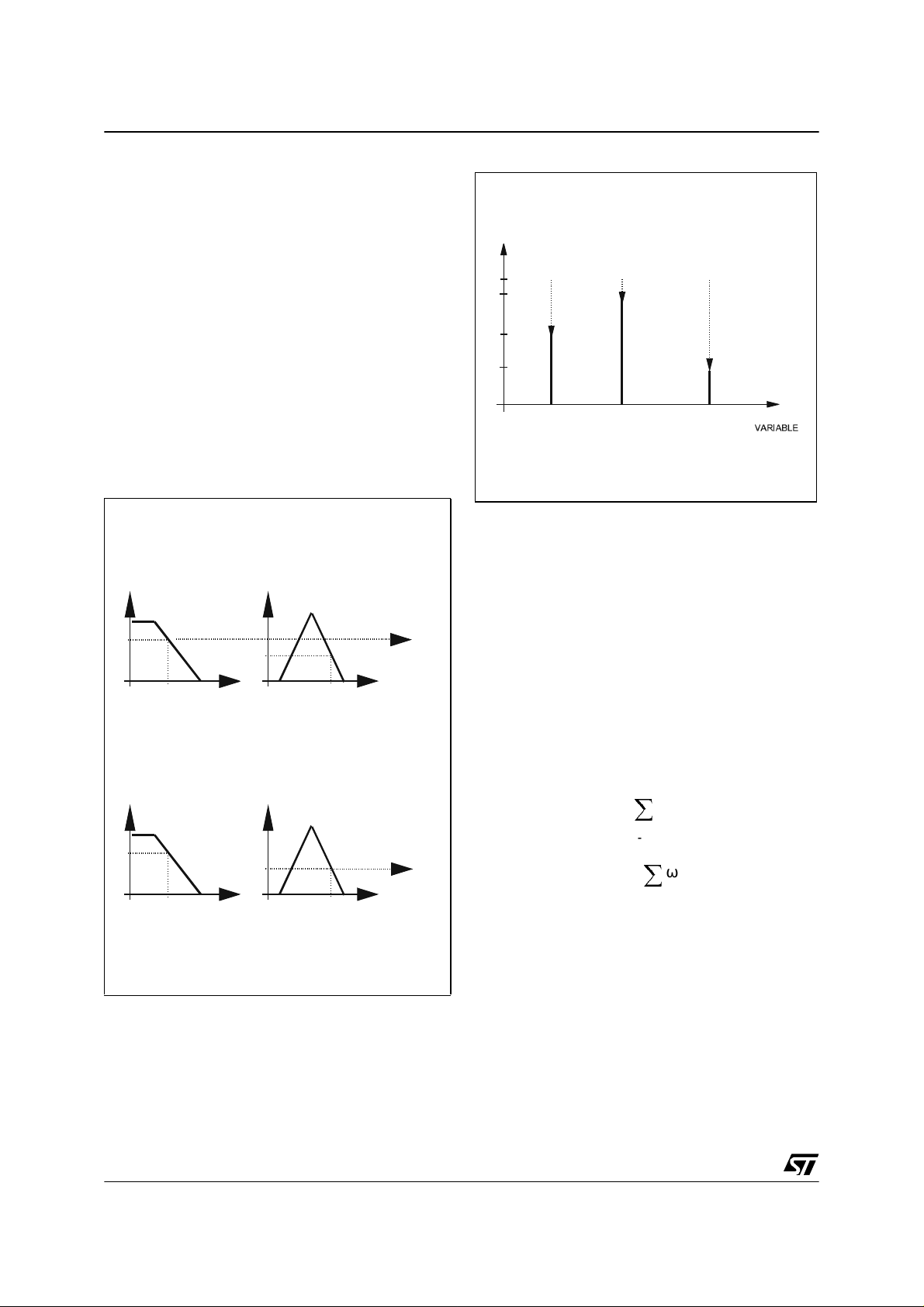
Figure 2.6 Alpha Weight Calculation
1
ij
α
2.3.2 Fuzzyfication Phase.
In this phase the in tersection (alpha weight)
between the input values and the related Mbfs is
performed (Figure 2.6).
8 Fuzzy input regist ers are available for fuzzy
inferences.
After loading the input values by using the LDFR
assembler instruction, the user can start fuzzynference by using the assembler instructionFUZZY.
During fuzzyfication: input data is transformed in
the activation level (alpha weight) ofthe Mbfs. i
j-th Mbf
i-th INPUT VARIABLE
Input Value
Figure 2.7 Fuzzy Inference
FUZZYFICATION
Input Values
11
1m
INFERENCE
n1
nm
PHASE
1
2
DEFUZZYFICATION
N rules -1
Nrules
Output Values
25/94
ST52T400/T440/E440/T441
X
2.3.3 Inference Phase.
The Inference Phase manages the alpha weights
obtained during the fuzzyfication phase to c ompute the truth value (
Ω) for each rule.
This is a calculation of th e maximum (for the OR
operator) and/or minimum (for the AND operator)
performed on alpha values according to the logical
connectives of fuzzy rules.
Several conditions may be linked together by linguistic con nec tive s AND/OR, NOT operator and
brackets.
The truth value ω and the related output singletonmove t o the Defuzzyfication phase in order to
complete the inferenc e calculation.
Figure 2.8 Fuzzyfication
IF
INPUT 1
1
IF
INPUT 1
1
IS X1 OR
X1
IS X1 AND
X1
Input 1
Input 1
INPUT 2
α2
OR = Max
INPUT 2
α2
IS X2 THEN .......
X2
Input 2
IS X2 THEN ......
X2
Input 2
Figure 2.9 Output Membership Functions
i0
j-th Singleton
ij
X
i-th OUTPUT
in
1
ω
ij
ω
i0
ω
in
0
X
2.3.4 Defuzzyfication.
In this phase the output crisp values are determined by implementing the conseq uent part of the
rules.
Each consequent Singleton X
weight values ω
, calculated by the Fuzzy Infer-
i
is multiplied by its
i
ence Unit, in order to compute the upper part of
the defuzzification.
Each output value is deduced from the consequent crisp values (X
) by carrying out the follow-
i
ing defuzzification formula:
where:
N
Xijω
j
N
∑
j
ij
ω
ij
Y
=
i
∑
--------------------- -
i = 0,1 ident ifies t he current output variable
N = number of the active rules on the current output
=weight of th e j-t h singleton
ω
ij
Xij = abscissa of the j-th singleton
Fuzzy outputs are stored in the RAM location i-th
specified in the assembler instruction OUT i.
26/94
ST52T400/T440/E440/T441
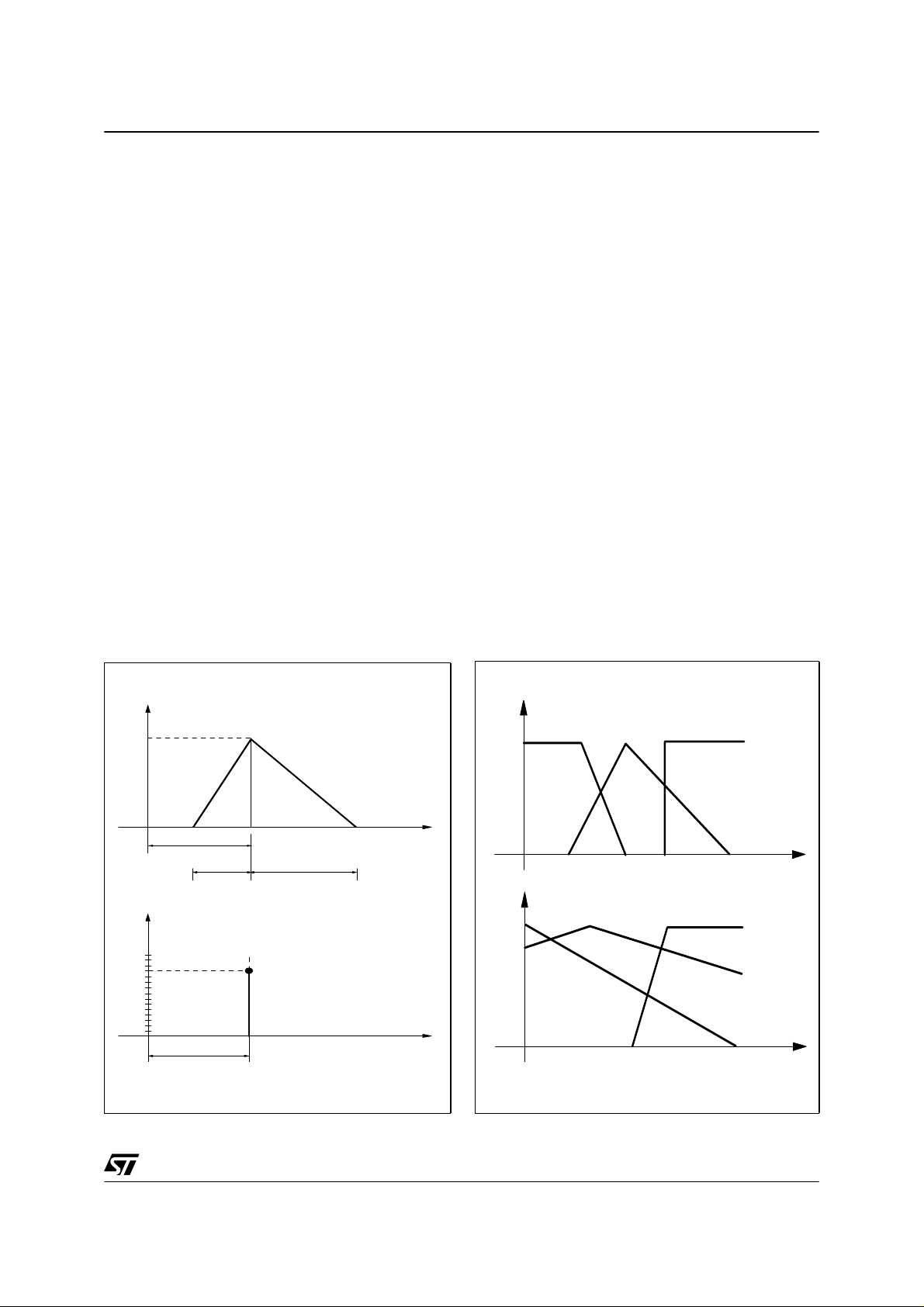
2.3.5 Input Membership Function.
ST FIVE allows the management of triangular
Mbfs. In order to define an Mbf, three different
types of data must be stored on the Program/Data
Memory:
the vertex of the Mbf: V;
the length of the left semi-base: LVD;
the length of the right semi-base: RVD;
In order to reduce the size of the memory area
and the computational effort the v ertical dimension
of the vertex is set to 15 (4 bits).
By using the previous memorization method different kinds of triangular Membership Functions ma y
be stored. Figure 4.6 illustrates a typical example
of Mbfs that c an be defined in ST FIVE.
Each Mbf is then defined storing 3 bytes in the first
1 Kbyte of the programmemory.
The Mbf is memorized by using the following
instruction:
MBF n_mbf lvd v rvd
where
n_mbf identifies Mbf, l v d, v, and rvd, which are the
parameters that describe the Mbf’s shape.
2.3.6 Output Singleton.
ST FIVE uses a particular kind of membership
function called Singleton for its output variables. A
Singleton doesn’t have a shape, like a traditional
Mbf, and is characterized by a single point identified by the coup le (X, w), where the w is calculated by the Inference Unit as described before.
Often, a Singleton is simply identified with its Crisp
Value X.
2.3.7 Fuzzy Rules.
Rules can have the following structures:
if A op B op C...........then Z
if (A op B) op (C op D op E...)...........then Z
where op is one of the possible linguistic operators (AND/OR)
In the first cas e the rule operators are managed
sequentially; in the second one, the priority of the
operator is fixed by the brackets.
Each rule is codified by using an instruction set,
the inference time for a rule with 4 antecedents
and 1 consequent is about 3 microseconds.
Figure 2.10 Mbfs Parameters
15
0
15
w
0
V
LVD R VD
X
Figure 2.11 Example of valid Mbfs
Input M bf
Input V ariable
Output S ingleton
Output Variable
27/94

ST52T400/T440/E440/T441
The assembler Instruction S et, which manages fu zzy instructions is reported in the following table:
Table 2.4 F uz z y Instruction Set
Instruction Description
MBF
n_mbf Ivd v rvd
LDP
nm
Stores the Mbf
Fixes the alpha value of the inputnwith the Mbfmand stores it in internal registers
n_mbf
with the shape identified by the parameters
Ivd,v
and
rvd
nm
LDN
FZAND
FZOR
LDK Stores the result of the last Fuzzy operation executed in internal registers
SKM
LDM Copies the value of register M in the data stack
crisp
CON
OUT
n_out
FUZZY Starts the Fuzzy algorithm
Calculates the complementary alpha value of the inputnwith the Mbfm. and stores the
result in internal registers
Implements the Fuzzy operation AND between the last two values stored in internal
registers
Implements the Fuzzy operation OR between the last two values stored in internal registers
Loads the result of the last performed Fuzzy operation (stored in the temporary register
K) in the temporary buffer M.
Multiplies the
Performs Defuzzyfication and stores the currently Fuzzy output in the RAM
crisp
value with the last ω weight
n_out
location
28/94

ST52T400/T440/E440/T441
Example 1:
IF Input
is codified by the foll owing instructions:
LDN 1 1 calculates the NOT α value of Input
LDP 4 12 fixes the α value of Input
FZAND adds the NO T α and α val ues obtained with the operations LDN1 1 and LDP 4 12
LDK stores th e r es ult of the operation FZAND in internal registers
LDP 3 8 fixes the α value of Input
FZOR implements the operation OR between the results obtained with the operations LDK and
LDP
CON crisp
Example 2, the priority of the operat or is fixed by the b rackets:
IF (Input
LDP 3 fixes the α value of Input3 with Mbf1 and stores the result in internal registers
LDN 4 15 calculates the NOT α value of Input
FZAND adds NOT α and α v alues obtained with the operations LDP 3 1 and LDN 4 15 SKM
LDP 1 6 fixes the α value of Input
LDN 2 14 calculates the NOT α value of Input
FZOR implements the operation OR between the α and NOT α values obtained with the two previ-
LDK stores th e r es ult of the operation OR in internal registers
LDM copies the value of the memory register M in internal registers
FZOR implements t he operation OR between the last two values stored in internal registers (LDK
CON crisp
IS NOT Mbf1AND Input4is Mbf12OR Input3IS Mbf8THEN Crisp
1
with Mbf1and stores the result in internal registers
1
with M12and stores the result in internal registers
4
with Mbf8and stores the result in internal registers
3
multiplies the result of the last Ω operation with the crisp value Crisp
1
IS Mbf1AND Input4IS NOT Mbf15)OR(Input1IS Mbf6OR Input6IS NOT Mbf14)THENCrisp
3
with Mbf15and stores the res ult in internal registers
4
1
1
stores the result of the operation FZAND in internal registers
with Mbf6and stores the result in internal registers
1
with Mbf14and stores the result in internal registers
6
ous operations (LDP 1 6 and LDN 2 14)
and LDM)
multiplies the result of the last Ω operation with the crisp value Crip
2
2
2
At the end of the fuzzy rul e, by using the instruction OUT RAM_reg, a byte is written. Afterwards, the control of the algorithm goes returns to the CU.
29/94

ST52T400/T440/E440/T441
2.4 Arithmetic Logic Unit
ST52x400/440/441 supplies 46 instructions that
perform comp utations and control the device.
Computational time required for each instruction
consists of one clock puls e for each Cycle plus 2
clock pulses for t he decoding phase. Total computation time for each instruction is reported in Table
2.5
The ALU of the ST52x400/440/441 can perform
multiplication (MULT) and division (DIV). Multiplication is performed by using 8 bit operands storing the result in 2 registers (16 bit values).
Division is performed between a 16 bit dividend
and an 8 bit divider, the result and the remainder
are stored in two 8-bit registers.
WARNING:
If the LSB of the multiplication result
is 0, the Zero flag is set although the result is not
0.
2.4.1 Addressing Modes.
ST52x400/440/441 instructions allow the following
addressing modes:
Inherent: this instruction type does not require an
operand because the opcode specifies all the
information necessary to carry out the instruction.
Examples: NOP, RET.
Immediate: these instructions have an operand a s
a source immediate value. Exampl es: LDRC,
PGSET.
Direct: th e operands of these instructions are
specified wi th the d irect addresses. The operands
can refer, accordi ng to the opcode, to addresses
belonging to the different addressing spaces.
Example: SUB, LDRE.
Indirect: data addresses tha t are required are
found in the locations specified as operands. Both
source and/or destination operands can be
addressed indirectly. The operands can refer,
(according to the opcode) to a ddres ses belonging
to different addressing spac es . Examples: LDRE
(reg1),(reg2).
2.4.2 Instruction Types.
ST FIVE supplies the following instruction types:
■ Load Instructions
■ Arithmetic and Logic Instructions
■ Jump Instructions
■ Interrupt Management Instructions
■ Control Instructions
The instructions are listed in Table 2.5, Table 2.6
and Table 2.7.
Table 2.5 Arithmetic & Logic Instruction Set
Load Instructions
Mnemonic Instruction Bytes Cycles Z S C
LDCE LDCE confx,memx 3 17 - - LDCR LDRC confx,regx 3 14 - - -
LDFR LDFR fuzzyx,regx 3 14 - - LDPE LDPE outx,memx 3 17 - - -
LDPE LDPE outx,(regx) 3 17 - - LDPR LDPR outx,regx 3 14 - - LDRC LDRC regx,const 3 14 - - LDRE LDRE regx,memx 3 16 - - LDRE LDRE (regx),(regy) 3 18 - - -
LDRI LDRI regx,inpx 3 15 - - -
LDRR LDRR regx, regy 3 16 - - -
PGSET PGSET const 2 9 - - -
30/94

ST52T400/T440/E440/T441
Table 2.6 Arith m etic and Logic Instruction Set (Continued)
Arithmetic Instructions
Mnemonic Instruction Bytes Cycles Z S C
ADD ADD regx, regy 3 17 I - I
ADDO ADDO regx, regy 3 20 I I I
AND AND regx, regy 3 17 I - -
ASL ASL regx 2 15 I - I
ASR ASR regx 2 15 I I DEC DEC regx 2 15 I I -
DIV DIV regx, regy 3 26 I I I
INC INC regx 2 15 I - I
MULT MULT regx, regy 3 19 I - -
NOT NOT regx 2 15 I - -
OR OR regx, regy 3 17 I - -
SUB SUB regx, regy 3 17 I I -
SUBO SUBO regx, regy 3 20 I I I
MIRROR MIRROR regx 2 15 I - -
Jump Instructions
Mnemonic Instruction Bytes Cycles Z S C
CALL CALL addr 3 18 - - -
JP JP addr 3 12 - - -
JPC JPC addr 3 10/12 - - -
JPNC JPNC addr 3 10/12 - - JPNS JPNS addr 3 10/12 - - JPNZ JPNZ addr 3 10/12 - - -
JPS JPS addr 3 10/12 - - -
JPZ JPZ addr 3 10/12 - - -
RET RET 1 13 - - -
Interrupt Instructions Set
Mnemonic Instruction Bytes Cycles Z S C
HALT HALT 1 7/15 - - MEGI MEGI 1 7/15 - - MDGI MDGI 1 6 - - -
RETI RETI 1 12 - - -
RINT RINT const 2 8 - - UDGI UDGI 1 6 - - UEGI UEGI 1 7/15 - - -
WAITI WAITI 1 7/14 - - -
31/94

ST52T400/T440/E440/T441
Table 2.7 Control Instructions Set
Control Instructions set
Mnemonic Instruction Bytes Cycles Z S C
FUZZY FUZZY 1 5 - - -
NOP NOP 1 6 - - WDTRFR WDTRFR 1 7 - - WDTSLP WDTSLP 1 6 - - -
Notes:
| flag affected
- flag not affected
regx, regy: Register File addresses
memx, memy: Program/Data Memory addresses
confx, confy: Configuration Registers addresses
outx: Output Regis ters addresses
inpx: Input Registers addres s es
const: constant value
fuzzyx: Fuzzy Input Register
addr: Program instructions address
Figure 2.12 Multiplication
RAM
0
1
2
i
j-1
j
j+ 1
253
254
255
REG. j REG. i
LSB
X
16Bit
MSB
Figure 2.13 Division
253
254
255
REG. j REG. j+1
REMAINDER QUOTIENT
i-1
i+1
j-1
j
j+1
RAM
0
1
2
i
:
REG. i
32/94

ST52T400/T440/E440/T441
3 EPROM PROGRAMMING
EPROM memory provides an on-chip user-programmable non-volatile memory, which all ows fast
and reliable storage of user data.
EPROM memory can b e locked by the user. In
fact, a memory location, called Lock Cell, is
devoted to lock t he EPROM and to prevent
Table 3.1 EPROM Control Register
OPERATION REGISTER VALUE
Stand By
Memory
Reading / Verify
Memory Unlock and
Lock Status Reading
Memory
Writing
Memory
Lock
ID CODE
Writing
Memory Lock Status
Reading / Verify
0
1
2
3
4
5
9
memory reading. A software id entifica tion code
(max 64 bytes), called ID CODE may also be written in order to distinguish whi ch software version
is stored in the memory.
There are 64 kbits of memory space with an 8-bit
internal parall elism (8 kbytes) addressed by a 13bit bus. The data bus is of 8 bits.
Memory has a double supply: V
12V±5% in Programming Phas e or to V
Working Phase. V
is equal to 5V±10%.
DD
is equal to
PP
SS
during
The ST52x400/440/441 EPROM m emory is
divided into three main blocks (see Figure 3.1):
•
Interrupt Vectors memory block
(3 through 14)
contains the addresses for the interrupt routines. Each address is composed of t hree
bytes.
•
Mbfs Setting memory block
(15 through 1024)
contains the c oordinates of the vertexes of
every Mbf defined in the program. If this part of
the memory is not used to s tore the M bfs setting, it can be use to store the instruction set on
the user program.
•
The Program Instruction Set mem ory block
(1024 t hrough 8191) contains the instruction
set of the us er program.
ID CODE
Reading / Verify
10
Figure 3.1 Program Memory Organization
2000h
PROGRAM INSTRUCTIONS
AND PERMANENT DATA
0400h
PROGRAM INSTRUCTIONS
AND PERMANENTDATA
0015h
0003h
0000h
MEMBERSHIP FUNCTIONS
PARAMETERS
INTERRUPT VECTORS
RESET VECTOR
33/94

ST52T400/T440/E440/T441
O
RYVERIFYMAR
GIN
E
ATA
A
TADATA
O
The locati ons 0, 1 and 2 contain the jump instruction to the first code line. This instruction is automatically inserted by the Assembler tool. The
operations that can be performed on EPROM during the Programming Phase are: Stand By, Memory Writing, Reading and Verify/Margin Mode,
Memory Lock, IDCode Writing and Verify.
The operations above are managed by using the
4-bit EPROM Control Register. The reading phase
is executed with V
Margin Mode phase needs V
=5V±5%, while the verify/
PP
= 12V±5%. The
PP
Blank Check must be a reading operation with
=5V±5%.
V
PP
Table 3.1 illustrates the EPROM Control Register
codes used to select the operation. Programming
of the EPROM Control Register is described
below.
3.1 EPROM Programming Phase Procedure
Programming mode is selected by applying
12V±5% voltage or 5V±5 % voltage to the V
PP
pin
and setting the RESET pin =Vss
If the V
voltage is 5V±5% only reading may be
PP
performed.
RST_ADD (PB0), INC_ADD (PB1), RST_CONF
(PB2), INC_CONF (PB3) and PHASE (PB7) are
the control signals applied during Programming
Mode.
The signals RST_ADD, RST_CO NF and P HA SE
are active on level, the others are active on rising
edge.
The signals RST_AD D a nd PHASE are active low,
signal on RST_CONF is active high.
Data in/out digital signals are t rans ferred through
thepinsofPortA.
The memory may be locked by means of the
Memory Lock Status flag, that is used to enable
EPROM operations.
If Memory Lock Status flag is 1 all EPROM operations are enabled, otherwise, it is only pos sible to
read (and verify) the OTP code and the Memory
Lock Status flag.
Only If EPROM is not locked by means of Lock
Cell (see paragraph EPROM Lo cki ng), may
EPROM operations be enabled, changing the
Memory Lock Status flag from 0 to 1.
The signal RST_ADD (PB0) resets the memory
address register and the Memory Lock Status flag.
Therefore, when the R ST _A DD becomes high,
the memory must be unlocked in order to read or
write.
The signal RST_CONF (PB2) resets the EPROM,
Figure 3 .2 EPROM Programming Timing
D
100nS
DATA
OUT
PA(0:7)
RST_ADD
RST_CONF
INC_ADD
INC_CONF
PHASE
MEMORY UNLOCK MEMORY WRITING
DATA D
DATA
LOCATION ADDRESS =1
DATA
IN
UT
10
S
µ
MEM
OUT
MOD
34/94

ST52T400/T440/E440/T441
INC_ADD (PB1) signal increments the memory
address.Control Register. When RST_CONF is
high, the DATA I/O Port A is in output, otherwise it is always in input.
The si gnal applied on INC_CONF (PB3) i nc rements the EPROM Control Register value. To
select the operation it must be provided as many
signal edges as the v alue to be writte n in the reg ister (see Table 3.1).
The signal on PHASE (PB 7) validates the operation selected by means of the EPROM Control
Register value.
3.1.1 E PROM Operati on. In order to execute an
EPROM operation (s ee Table 3.1), t he corresponding identification value must be loaded in
the EPROM Control Register. The signal timing is
the following: RST_ADD= high and PHASE= high,
RST_CONF changes f r om low to high level, to
reset the EPROM Control Register, and
INC_CONF signa l generates a number of po sitive
pulses equal to the value to be loaded. After this
sequence, a negative pulse of the PHASE signal
will vali date the selected ope ratio n. The minimum
PHASE signal pulse width must be 10 µsforthe
EPROM Writing O peration and 100 ns for the others.
When RST _CONF is high, the DATA I/O Port A is
enabled in output and the reading/verify operat ion
results are available.
After a writing operation, when RST_CONF is
high, Port A is in output without valid data.
3.1.2 E PROM Locking. The Memory Lock operation, which is identified with the number 4 in the
EPROM Control Register, writes “0" in the Memory Lock Cell.
At the beginning of an External Operation, when
RST_ADD signal changes from low level to high
level, the Memory Lock Status flag is “0", therefore
it is necessary to unlock it before proceeding.
In order to unlock the Memory Lock Status flag the
operation, which is identified with t he numbe r 2 in
the EPROM Control Register must be executed
(see Figure 3.2).
The Memory Lock Status flag can be c hanged.
Therefore, after a Memory Lock operation, external operations cannot be executed except reading
(or verify) the OTP Code and the Memory Lock
Status.
3.1.3 EPROM W riting. When the memory is
blank, all the bits are at logic level “1". The data is
introduced by programming only the zeros in the
desired memory location; however, all input data
must contain both ”1” and “0". The only way to
change “0" into ”1” is to erase t he whole memory
(by exposure to UV light) and reprogram it.
The memory is in Writing mode when the EPROM
Control Register value is 3.
The V
voltage must be 12V±5%, with stable
PP
data on the data bus PB(0:7). The signals timing is
the following (see Figure 3.2):
1) RST_ADD and RST_CONF change from low to
high level,
2) two pulses on INC_CONF signal load the Memory Unlock operation code,
3) a negative pulse (100 ns) on the PHASE signal
validates the Memory Unlock operat ion,
4) a negative pulse on RST_CONF signal resets
the EPROM Control Register,
5) three positive pulses on INC_CONF load the
Memory Writing operation code,
6) a train of positive pulses on INC_AD D signal
increments the memory location address up to the
requested value (generally this is a sequential
operation and only one pulse is used),
7) a negative pulse (10 µs) on the PHA S E s ignal
validates the Memory Writing operation.
3.1.4 EPROM Reading/Verify Margin Mode.
ThereadingphaseisexecutedwithV
instead of veri fy phase that needs V
=5V±5% ,
PP
=12V±5%.
PP
The Memory Verify operation is available in order
to verify the co rrectness of the data written. The
Memory Verify M argin Mode operation may be
executed immediately after the writing of eac h
byte and in this case (see Figure 3.2):
1) one positive pulse on RST_CONF signal res ets
the Control Regist er, if it was not already reset
2) one positive pulse on INC_CONF loads the
Memory Reading/Verify operation code,
3) one negative pulse (100 ns) on the PHASE signal validates the Memory Reading/Verify operation,
4) a negative pulse on RST_CONF s ignal puts in
the PB (0:7) port the value stored in the actual
memory address and resets the EPROM Control
Register.
Then, if any error in w riting occurred, the user has
to repeat the EPROM writing.
35/94

ST52T400/T440/E440/T441
3.1.5 Stand by Mode. E PROM has a standby
mode which reduces the active current from 10mA
(Programming mode) to less than 100 µA. Memory is placed in standby mode by setting P HASE
signal at high level or when the EPROM Control
Register value is 0 and PHASE signal is low.
3.1.6 ID code. A software identification code,
called ID code may be written to di stinguish which
software version is stored in the memory.
64 Bytes are dedicated to store this code by using
the address values from 0 to 63.
The ID Code may be read or verified even if the
Memory Lock Status is “0".
The signals timing is the same as that of a normal
operation.
3.2 Eprom Erasure
Thanks to the t rans parent window available i n the
CDIP28W package , its memory contents may be
erased by exposure to UV light.
Erasure begins when the device is expose d to
light with a wavelength shorter than 4000Å. It
should be noted that sunlight, as well as some
types of artificial light, includes wavelengths in the
3000-4000Å range which, on prolonged expos ure,
can cause erasure of memory contents. It is thus
recommended that EPROM devices be fitted with
an opaque label over the window area in order to
prevent unintentional eras ure.
The recommended erasure procedure f or EPROM
devices consists of exposure to short wave UV
light having a wavelength of 2537Å. The min imum
recommended integrated dose (intensity x expo-
sure time) for compl ete erasure is 15Wsec/cm
This is equi v alent to an erasure time of 5-10 minutes using a UV source having an intensity of
12mW/cm
2
at a distance of 25mm (1 inch) from
the device window.
2
.
36/94

4 INTERRUPTS
IAC/FI
/
P
NT_EX
T15161718
9
0INT_T
RIAC/PR
T
NTER
R
S
R
T
I
O
The Cont rol Unit (CU) responds to peripheral
events and external events v ia its interrupt channels.
When such an events occur, if the related interrupt
is not mas k ed and acc ording to a priority order,
the current program execution can be suspended
to allow the CU to execute a specific response
routine.
Each interrupt is associated with an interrupt vector that contains the memory addres s of the
related interrupt service routine. Each vector i s
located in t he Program Space (EPROM Memory)
at a fixed address (see Interrupt Vectors Figure
4.2).
4.1 Interrupt Operation
If there are pending interrupts at the end of an
arithmetic or logic instruc tion, the one with the
highest priority is passed. Passing an interrupt
means to store the arithmetic flags and the current
PC in the stack and execute the associated Interrupt routine, whose address is l oc ated in three
bytes of the E PROM memory location between
address 3 and 20.
The Interrupt routine is perform ed as a normal
code checking, at the end of eac h instruction, if a
higher priority interrupt has to be passed. An Interrupt request with the higher priority stops the
lower priority Interrupt. The Program Counter and
the arithmetic flags are stored in the stack.
With the instruction RETI (Return from Interrupt)
the arithmetic flags and Program Counter (PC) are
restored from the t op of the stack, which was previously described in Section 2.2.1.
An Interrupt request cannot stop fuzzy rule processing, but this is passed o nly after the end of a
fuzzy rule or at the end of a logic, or arithm eti c
instruction.
REMARK:
A fuzzy routine can be interrupted only
in the Main program. Wh en a Fuzzy function is
running inside another interrupt routine an interrupt request can cause side effects in the Control
Unit. For this reason, inorder to use a Fuzzyfunction inside an interrupt routine, the user MUST
include the Fuzzy function between an UDGI
(MDGI) i nstruction and and UEGI (MEGI) instruction (see the following paragraphs), in order to disable the interrupt request during the execution of
the fuzzy function.
ST52T400/T440/E440/T441
Figure 4.1 Interrupt Flow
NORMAL
PROGRAM
FLOW
I
UPT
ERVICE
OUTINE
INTERRUPT
RETI
INS
RUCT
N
Figure 4.2 Interrupt Vectors Mapping
0
1
ESE
2
3
4
INT_AC
5
6
7
8
9
10
11
12
13
14
1
2
NT_TIMER
INT_TR
INT_TRIAC/R
I
WM
INTERRUPT
VECTORS
Figure 4.3 Global Interrupt Request Generation
Global Interrupt
Pending
Global I nterrupt
Request
User Global
Interrupt Mask
Macro Global
37/94

ST52T400/T440/E440/T441
4.2 Global Interrupt Request Enabling
When an Interrupt occurs, it generates a Global
Interrupt Pending (GIP), which can be m as k ed by
software. After a GIP, a Global Interru pt Request
(GIR) will be generated a nd an Interrupt Service
Routine associated to the interrupt with higher priority will start. I n order to avoid possibl e conflicts
between interrupt masking set in the main program, or inside macros, the GIP is masked
through the User Global Interrupt Mask or the
Macro Global Interrupt Mask (see Figure 4.3).
UEGI/UDGI instruction switches the User Gl obal
Interrupt Mask on/off, enabling/disabling the GIR
for the main program.
MEGI/MDGI instructions switches the Macro Global Interrupt Mask on/off in order to ensure t hat
the macro will not be broken.
4.3 Interrupt Sources
ST52x400/440/441 manages interrupt s ignals
generated by the interna l peripherals (PWM/
TIMER, TRIAC Driver and Analog Comparator) or
deriving from t he External Interrupt on pin PA7.
The External Interrupt can be programmed to be
active on the risin g or f all ing edge of INT/PA7 signal by settin g the PEXTINT b it of the Configuration Register to0.
WARNING:
interrupt request is generated.
Each peripheral ca n be programmed in order to
generate the associated interrupt; further details
are described in t he related chapter.Configuration
Register 0 is also used to enable/disable the
Brown-Out (see the related chapter).
Changing the interrupt priority an
Table 4.1 Configuration Register 0
Description
Bit Name Value Description
0
0 MSKE
1
0
1 MSKAC(*)
1
0
2 MSKTM
1
0
3 MSKTRF
1
0
4 MSKTRR
1
External Interrupt
Masked
External Interrupt
Not Masked
Analog
Comparator
Interrupt
Masked
Analog
Comparator
Interrupt Not
Masked
PWM/TIMER
Interrupt
Masked
PWM/TIMER
Interrupt
Not Masked
TRIAC Falling
Edge Interrupt
TRIAC Falling
Edge Interrupt
Not Masked
TRIAC Rising
Edge Interrupt
Masked
TRIAC Rising
Edge Interrupt
Not Masked
4.4 Interrupt Maskability
The interrupts can be masked by configuring the
Configuration Register 0 by me ans of an LDCR or
an LDCE instruction. The interrupt is enabled
when the bit ass oc iated to the mask interrupt is
“1". V icev ersa , when the bit is ”0", the interrupt is
masked and is kept pending.
For example:
LDRC 10,6 (loads the cons tant 6 in the RAM
Register 10)
LDCR 0,10 (sets REG_CONF0 with the value
stored in RAM Register 10)
the result is REG_CONF0=00000110, enabling
the interrupts coming from the Anal og Comparator
(INT_AC) and from the PWM/TIMER (INT_PWM/
TIMER).
38/94
0
5 MSKTRP
1
0
6 PEXTINT
1
0
7 MSKBR
1
Reset Configuration ‘00000000’
(*) Not Used in ST52x400 devices
TRIAC Pulse
Interrupt Masked
TRIAC Pulse
Interrupt Not
Masked
External
Interrupt active
on Rising Edge
External
Interrupt active
on Falling Edge
Brown-Out
Disabled
Brown-Out
Enabled

Table 4.2 Interrupts Description
ST52T400/T440/E440/T441
Name Description Priority
INT_AC(*) Analog Comparator Int Programmable 000 yes 3-5
INT_PWM/TIMER PWM/TIMER Int Programmable 001 yes 6-8
INT_TRIAC/F TRIAC Falling Edge Int Programmable 010 yes 9-11
INT_TRIAC/R TRIAC rising edge Int Programmable 011 yes 12-14
INT_TRIAC/P TRIAC Pulse Int Programmable 100 yes 15-17
INT_EXT External Interrupt (INT) Ext Highest - yes 18-20
(*) Used only in ST52x440/441 devices
Figure 4.4 Interrupt Configuration Register 0
Peripheral
Code
Mask-
able
REG_CONF0
Interrupts Mask
Vector
Addresses
D7 D6 D5 D4 D3 D2 D1 D0
MSKE: Ex t. Int.
MSKAC: An. Comp . Int.
MSKTM: Timer Int.
MSKTRF: Tri ac Fall. Int.
MSK TRR: Triac Ris. Int.
MSKTRP: Triac Pulse I nt.
PEXTINT: Ext. Int. Ris/Fall.
MSKBR: Brown Out En.
39/94

ST52T400/T440/E440/T441
Figure 4.5 Interrupt Configuration Registers 17 and 18
Inte rrup tsPriority
REG_CON F18
D10D11D12D13D14D15
4.5 Interrupt Priority
Seven priority levels are available: level 6 has the
lowest priority, level 0 has the highest priority.
Level 6 is ass oc iat ed to the Main Program, levels
5 to 1 are programmable by means of the priority
registers called REG_CONF17 and
REG_CONF18; whereas the higher level is
related to the External Interrupt (INT_EXT).
PWM/Timer, TRIAC/P WM and Analog Block are
identified by a three-bit Peripheral Code (see
Table 4.2); in order to set the
user must write t he peripheral label
INT
i
priority level.
i
-th priority level the
D8
D9
i
in the rela ted
REG_CONF17
D0
D1D2D3D4D5D6D7
INT1
INT2
INT3
INT4
INT5
Not Used
■ Level 5: INT_T R IAC/PWM_F (TRIAC/PWM_F
Code: 010)
Table 4.3 Conf. R egisters 17-18 Description
Bit Name Value Level
0, 1, 2 INT1 Peripheral High
3, 4, 5 INT2 Peripheral MediumHigh
6, 7, 8 INT4 Peripheral MediumLow
9, 10, 11 INT5 Peripheral Low
12, 13, INT6 Peripheral Very Low
For instance:
LDRC 10,193 (loads the value 193=’11000001’
in the RAM Register 10)
LDRC 11,168 (loads the value 168=’10101000’
in the RAM Register 11)
LDCR 17,10 (REG_CONF17= ‘11000001’)
LDCR 18,11 (REG_CONF18= ‘10101000’)
thus defining the following priority levels:
■ Level 1: INT_PWM/TIMER(PWM/TI ME R Code:
001)
■ Level 2: INT_ADC ( ADC Code: 000)
■ Level 3: INT_TRIAC /PWM_R (TRIAC/PWM
Code: 011)
■ Lev el 4: INT_TRIAC/Ph (TRIAC/Ph C ode: 100)
40/94
REMARK:
The Interruptprioritymust beset at the
beginning of the main progra m, because at the
RESET REG_CONF1=’00000000’, this condition
could generate wrong operations. F urthe r,
changing the priority levels must be avoided in
interrupt service routines.
When a source provides an Interrupt reques t, and
the request processing is also enabled, the CU
changes the norm al sequential flow of a program
by transferring program cont rol to a selected service routine.
When a n interrupt occurs the CU executes a
JUMP instruction to the address loaded in the
related location of the Interrupt Vector and the
flags are saved.
When the execution ret urns to th e original pro-

ST52T400/T440/E440/T441
gram, the flags are restored and the program continues from the instruction immediately f ollowing
the interrupted instruction.
4.6 Interrupts and Low power mode
All interrupts allow the proc es so r to leave WAIT
mode. Only an External Interrupt request allows
the processor to leave HALT mode: if the interrupt
is masked, the related interrupt routine is not serviced and the program continues from the first
instruction after the HALT instruction.
4.7 Interrupt RESET
When an interrupt reques t is sent but the interrupt
is masked, it isn’t service d and remains pending,
so that when t he interrupt is enabled it is serviced
immediately. In order to avoid this from happening, the pending interrupt request can be res et
with the instruction RINT j, wh ich resets the
interrupt
j
-th wherejidentify the peripherals as
described in the follo wing table (see Table 4.4).
The assembler instruction:
RINT 2
Resets the TRIAC/PWM_F interrupt.
WARNING:
If an interrupt is reset, with the RINT
instruction within its own interrupt routine, the
priority level of the interrupt becomes the lowest
and the routine can be i mmediately interrupted by
a lower priority interrupt request.
Table 4.4 RINT Instruction Code
Peripheral Name Value
Analog Comparator (*) 0
PWM/TIMER 1
TRIAC/F 2
INT_TRIAC/R 3
INT_TRIAC/P 4
External Interrupt 5
(*) Not Used in ST52x400 devices
Figure 4.6 Example of a sequence of Interrupt Requests
PRIORITY
LEVEL
0
1
2
3
4
5
INT2 INT0 INT4 INT1 INT3
INT0
INT1
INT2
INT2
INT2
INT3
INT4
6
MAIN PROGRAM
MAIN PROGRAM
41/94

ST52T400/T440/E440/T441
K
5 CLOCK, RESET & POWER SAVING MODE
5.1 Clock System
The ST52x400/440/441 Clock Generator module
generates the internal clock for the internal Control Unit, ALU and on-chip peripherals and is
designed to require a minimum of external components.
The ST52x400 /44 0/441 oscillator circuit generates an internal clock signal with the s ame period
and phas e as at the OSCin input pin. The maximum frequency allowed is 20 MHz.
The system clock may be generated by using
either a quartz crystal, ceramic resonator (CERALOC), or an external clock.
Figure 5.1 Oscillator Connections
The different c lock generator options connection
methods are illustrated in Oscillator Connections.When an external clock is used, it must be
connected to the pin OSCin while OSCout should
be left floating.
The crystal oscillator start-up time is a function of
many variab les: crystal parameters (es pecially
R
), oscillator load capacitance (CL), IC parame-
s
ters, environment temperature, supply voltage.
It must be observed that the crystal or ceram ic
lead and circuit connections mu st be as short as
possible. Typical values for CL1, CL2 are 10pF for
a20MHzcrystal.
CRYSTAL CLOCK EXTERNAL CLOCK
ST52X440
OSCin OSCout
Cl1
10pF
Cl2
10pF
ST52X440
OSCin
CLOC
INPUT
OSCout
42/94

ST52T400/T440/E440/T441
N
ALRESE
T
E
SETBROWN-O
T
5.2 Reset
There are four sources of Reset:
- RESET pin (external source)
- WATCHDOG (internal source)
- POWER ON Reset (Internal s ourc e)
- BROWN OU T Reset (Internal source)
When a Reset event happens, all the registers are
set to the reset value and the user program
restarts from the beginning.
5.2.1 External Reset.
The Reset pin is an input pin. An internal res et
does not affect this pin.
A Reset signal originated by external sou rces is
recognized istantaneously. The RE SET pin may
be used to ensure Vdd has risen to a point where
the MCU can operat e correctly before the user
program is run. In working mode the R es et must
be set to ‘1’ (see Table 1.1)
5.2.2 Reset Operation.
The duration of a RESET c ondition is fixed at
1.000.000 internal CPU clock cycles (or 4096 in
case of BOD).
Following a Power-On Reset ev ent , or after exiting Halt Mode, a 1.000.000 CPU clock cycle delay
period is initiated in order to allow the oscillator to
stabilize and to ensure that recovery has taken
place from the Reset state.
A Pull up resistor of 100 KΩ guarantees that
RESET pin is at level “1” when no HALT or
Power-On events occurred.
If an external resistor is connected to the RESET
pin a minimum value of 10KΩ must be used.
After a RESET procedure is completed, the core
reads the instruction stored in the first 3 bytes of
the EPROM, w hich contains a JUMP instruction to
the EPR OM address containing th e first instruction of the user program. The Assembler tool automatically generates thi s J ump instruction with the
first instruction address.
5.2.3 Power-on Reset (POR).
A Power-On Reset is generated by an on-chip
detection circuit. This circuit ensures that the
device is not started until Vdd has reached the
nominal level of 2.3V and allows the c lock oscillator to stabilize.
Once 2.3V are reached, the Power-On circuit generates an internal RST s ignal that releases the
internal reset to the CPU and invokes a delay
counter of 1.000.000 CPU clock cycles, during
which the device is kept in RESET after Vdd has
risen.
A correct operation of Power-on detector is guaranteed if the slew rate of Vdd is 0.05 V/ms.
Note:
The power s upply must fall below 0 V for
the internal POR circuit to detec t the next rise of
Vdd.
At power on the POR is enabled by default.
POR is des igned exclusively to cope with powerup conditions and should not be used to detect a
drop in the power supply voltage, fo r which the
Brown-out Detector can be used instead.
Figure 5.2 Reset Block Diagram
RESET
Vdd
POWER-ON
RESET
Vdd
Vdd
BROWN-
OUT
WATCHDOG
COUNTER x
1.000.000
COUNTER x
4096
WA
CHDOG R
UT RESE
INTER
T
43/94

ST52T400/T440/E440/T441
5.2.4 Br ow n-Ou t Detector (BOD).
The on-chip Brown-Out Detector circuit prevents
the processor from f alling into an unpredictable
state if the power supply drops below a c ertain
level.
When Vdd drops below the Brown-out detection
level, the B rown-out causes an internal processor reset RST tha t remains active as long as Vdd
remainsbelow the Brown-Out Trigger Level.
Brown-Out resets the entire device except the
Power-on Detector and the Brown-out itself.
Enabling/disabling the B row n-out detector can be
performed by setting the software of the c ont rol bit
BOD of REG_CONF0 (Table 4.1).
When Vdd increases above the Trigger Level, the
Brown-Out reset is turned off after a delay of 4096
CPU clock cycles, which ensures stabilization of
the oscillator.
The Brown-Out falling voltage level typical value is
3.8V and the corresponding rising voltag e activation level is 4.1V.
A minimu m hysteresis of 250mV for the trigger is
guaranteed for spike free brown-out detection.
Brown-Out circuit detects a drop if V dd voltage
stays below the safe threshold for longer than 100
Clock cycles before activation/deactivation of the
Brown-Out in orde r to filter voltage spikes.
Brown-Out function is disabled by default and is
not active when in HALT mode.
5.3.2 Halt Mode.
Halt mode is the MCU’s lowest power consumption mode, which is entered by executing the
HALT instruction. The internal oscillator is turned
off, causing all internal processing t o be s topped,
including the operations of the o n-chip peripherals.
Halt mode cannot be used when the watchdo g
is enabled. If the HALT instruction is executed
while the watchdog system is enab led, it will be
skipped wi tho ut modifying the normal CPU operations.
TheICUcanexitHaltmodeafteranexternalinterrupt or reset. The oscillator is then turned on and
stabilization time i s provided bef ore restarting
CPU operations. Stabilization time is 4096 CPU
clock cycles after t he interrupt and 1 .000.000 after
the Reset.
After the s tart up delay, the CPU restarts operations by serving the external interrupt routine.
Reset makes the ICU exit from HALT mode and
restart, after the delay, from the beginning of the
user program after the delay.
Warning:
if the External Interrupt is disabled, the
ICU exits from the Halt mode and jumps to the
lower priority interrupt routine.
Figure 5.3 WAIT Flow Chart
Remark:
for higher frequencies, the device needs
Supply Voltage higher than the BOD threshold.
For this reason the BOD cannot work in this range
of frequencies. See Electrical Characteristic
Chapter in this Datasheet.
5.3 Power Saving Modes
There are two P ower Saving modes: WAIT and
HALT mode. These conditions may be entered by
using the WAIT and HA LT instructions.
5.3.1 Wait Mode.
Wait mode places the MCU in a low power consumption by stopping the CPU. All peripherals and
the watch dog remain active. During WAIT mode,
the Interrupts are enabled. The MCU will remain in
Wait mode until an Interrupt or a RESET occurs,
whereupon the P r ogram jumps to the interrupt
service routine or, if a RESET occurs, at the
beginning of the user program.
Remark:
44/94
in Wait mode the CPU c lock does’t stop.

Figure 5.4 HALT Flow Chart
ST52T400/T440/E440/T441
HALT INSTRUCTION
YES
HALT INSTRUCTION
SKIPPED
OSCILLATOR OFF
PERIPHERALS CLOCK OFF
CPU CLOCK OFF
NO
RESET
YES
OSCILLATOR ON
PERIPHERALS CLOCK ON
CPU CLOCK ON
1000000 CPU CLOCK
CYCLES DELAY
NO
WATCHDOG
ENABLED
NO
EXTERNAL
INTERRUPT
YES
OSCILLATOR ON
PERIPHERALSCLOCK ON
CPU CLOCK ON
4096 CPU CLOCK
CYCLES DELAY
RESET CPU
AND RESTART
USER PROGRAM
NO
RESTART PROGRAM
SERVICING THE
LOWER PRIORITY
INTERRUPT ROUTINE
EXTERNAL
INTERRUPT
ENABLED
YES
RESTART PROGRAM
SERVICING THE
EXTERNAL
INTERRUPT ROUTINE
45/94

ST52T400/T440/E440/T441
6I/OPORTS
6.1 Introduction
ST52x400/440/441 devices offer f lexible individually programmable multi-func ti onal input/output
lines. Refer to Chapter 1 for specific pin allocations.
21 I/O lines, grouped in 3 different ports, are available for ST52x400G/440G/441G devices:
PORT A = 8-bit ports (PA0 - PA7 pins)
PORT B = 8-b it ports (PB0 - PB7 pins)
PORT C = 5-bit port (PC0 - PC4 pins)
13 I/O lines, grouped in 2 different ports are available for ST52x400F/440F/441F devices:
PORT A = 8-bit ports (PA0 - PA7 pins)
PORT B = 5 -bit ports (PB0 - PB3 and PB7 pins)
These I/O lines can be programmed to provide
Digital Input/Output or Analog Input , or to connect
input/output signals to the on-chip peripherals a s
Alternate Pin Functions.
The input buffers are TTL compatible with Schmitt
Trigger in ports A and C while port B is CMOS
compatible without Schmit t trigger and it is used
for the Analog Inputs.
The output buffer ca n s upply up to 8 mA.
All the port pins of 400/440 devices have an
internal pull-up resistor (22
kΩ). The 441 device
doesn’t have inter nal pull-up resistor. This
pull-up resistor is automatically excluded
when th e pin is configured as Analog Input or,
in MAIN1 and MAIN2 pins, when the Triac
Driver is configured in Phase An gle Partialization or Burst mode.
Each single port pin can be programmed in input
or output or Alte rnate Function, so that in the
same port there can be both input and output pins.
The port pins are write/read in parallel at the same
time: when reading output pins, the port buffer
contents are read; when writing an input pin the
value is written in the buffer.
Each port is configured by u sing Configuration
Registers indicated in Table 6.1. The first is used
to define if a pin is an Input or an Output, t he second defines the Alternate functions.
Table 6.1 I/O Port Configuration Register
PORT A PORT B
Reg_Conf 4 Reg_Conf 13 Reg_Conf 11
Reg_Conf 12 Reg_Conf 14
Reg_Conf 11**
(*)
Not available in ST52x400F/440F/441F
PORT C
(*)
(**) Only in ST52x440F/441F
Figure 6.1 Ports A and C Functional Blocks
TO INPUTREGISTER
and PERIPHERALS
FROM PERIPHERAL
FROM OUTPUT REGISTER
FROM CONFIGURATION REGISTER
FROM CONFIGURATION REGISTER
46/94
TTL
Vcc
22 k
PORT A PIN
or PORT C PIN

Figure 6.2 Port B Functional Blocks
ST52T400/T440/E440/T441
Vcc
FROMCONFIGURATION REGISTER
TO INPUT REGISTER
TO A/D CONVERTER
FROM OUTPUT REGISTERS
FROM CONFIGURATION REGISTER
6.2 Input Mode
The input configuration is selected setting the corresponding configuration register bit in
REG_CONF4, REG_CONF13 and, where applicable, REG_CONF11 (see Paragraph I/O Port
Configuration Registers) to “1”. To use Port A and
B pins as digital input, the corresponding bits in
REG_CONF12 and REG_ CONF14 must be set
according to th e values shown in Table 6.4, Table
6.5 and Table 6.6.
Table 6.2 Input Register and I/O Ports
PORT A PORT B
IR 14 IR 15 IR 16
(*)
Not used for ST52x400F/440F/441F
PORT C
(*)
Table 6.3 Output Register and I/O Ports
PORT A PORT B
OR 0 OR 1 OR 2
(*)
Not used for ST52x400F/440F/441F
PORT C
(*)
Digital input data is automatica lly stored in
22 k
CMOS
PORT B PIN
the Input Registers (see Table 6.2), but the single
bit of the Input Register (IR) c annot be read
directly an d the value in a RAM location must be
copied. Digital data is stored in a RAM location by
using the assembler instruction:
LDRI regx,inpy
Then, each single bit can be examined by using
AND and OR operators with a suited mask value.
6.3 Output Mode
The output pin configuration is selected by set ting
the corresponding configuration registe r bit to “0”
(REG_CONF4, REG_CONF13 and, where applicable, REG_CONF11) (see paragraph I/O Port
Configuration Registers). in order to use Port A
and B pins as digital output, the corresponding bits
in REG_CONF12 and REG_CONF14 must be set
according to the values illustrated in Tables - Port
A - REG_CONF 4, - P ort A - REG_CONF 12 and
Analog Inputs REG_CONF 14.
Digital data is transferred to the related I/O Port by
means of the Output register (see Table 6.3), by
using the assembler instructions LDPE or LDPR
that respec t ively take the value to be transferred
to the ports from EPROM and RAM.
47/94

ST52T400/T440/E440/T441
6.4 Alternate Functions.
Port A and B pins in ST52x 400/440/441 are configurabletobeusedwithdifferentfunctions(Alternate Functions) rel ated to the use of peripherals.
Toconfigure a pin in Alternat e Functi on the rela ted
configuration registers must be set according to
the values shown in Tables - Port A - REG_CONF
4, - Port A - REG_CONF 12 and Analog Inputs
REG_CONF 14.
For example: if pin PA5/TCLK has to be used as
an external PWM/Timer Clock, REG_CONF4[(5)]
bit must be s et to ‘1’.
When the signal is an input of an on-chip
peripheral, the related I/O pin has to be configured in Input Mo de.
When a pin of Port B is used as an Analog Input,
the related I/O pin is automatica lly set in threestate. The analog multiplexer (controlled by the
Analog Comparator Configuration R egist er)
switches the analog voltage pres ent on the
selected pin to the common analog rail, which is
connected to the ADC input.
It is recommended that the voltage level or loading
on any port pin not b e changed while conversion
is running. Furthermore, it is recommended not to
have clocking pins located close to a selected
analog pin.
Timer/PWM Alternate Functions
Pins of Port A can be configured to be I/Os of the
on-chip TIME R /PWM of ST52x 400/440/441. The
configuration of these pins is performed by using
Configuration Re gisters REG_CONF4 and
REG_CONF12 (Tables - Port A - REG_CONF 4
and - Port A - REG_CONF 12).
If a pin has to be a TIMER Input (TSTRT, TCLK,
TRES) the related bit of REG_CONF4 must be set
to “1” and of REG_CONF12 mu st be set to “1”.
If, instead it must be a TIMER Output (TOUT,
TOUTN), REG_CONF12 re lated bit must be set to
“0” and the related bit of REG_CO N F4 be set to
“0”.
TRIAC Driver Alternate Function
When using the on-chip TRIAC, to have the
TRIAC Output on pin PA0, bit REG_CONF12[0]
must be set to “0” and REG_CONF4[0] to “0”.
When a s y nc hronizat ion with the Mains voltage is
necessary, in case either the Phase Angle Partialization or the Burst Modes is chosen, to have
MAIN1 and MAIN2 as Inputs on PortA, it is necessarytosetbits1and2ofREG_CONF4to“1”.
Table6.4 -PortA-REG_CONF4
6.5 I/O Port Configuration Regi sters
The I/O mo de for each bit of the three ports are
selected by using Con figuration Registers 4, 12,
13 and 11 (Table 6.1). The structure of these registers is illustrated in tables - Port A - REG_CONF
4, - Port A - REG_CON F 12, - Port B REG_CONF 13, Analog Inputs REG_CONF 14
and - Port C - REG_CONF 11. Each bit of the configuration registers sets the I/O mode of the
related port pin.
Analog Comparator Inputs
Pins PB0-PB7 for ST52x440G/441G and PB0PB3 and PB7 in ST52x440F/441F can be configured to be Analog Inputs by se tting the related bit
in REG_CONF 14 to “1” (Table 6.7) and the
related bit in REG_CONF13 to “1” (Table 6.6).
These analog inputs are connec ted to the on chip
Analog Comparator.
If the B andGap Reference (BG) is needed as an
Output for ST52x440G/441G REG _CONF13[6]
must be set to “0” and REG_CONF 14[6] to “1”.
Bit Name Value Pin Description
0D0 X PA0
1 D1 X PA1/MAIN1
2 D2 X PA2/MAIN2
3 D3 X PA3/ACSTRT(*)
4 D4 X PA4/TSTRT
5 D5 X PA5/TCLK
6 D6 X PA6/TRES
7 D7 X PA7/INT
X = 0 Pin set as Digital Output
X = 1 Pin set as Alternate Function Input
(
*) Not available in ST52x400xx
Reset Configuration ‘1111’
48/94

ST52T400/T440/E440/T441
Table6.5 -PortA-REG_CONF12
Bit Name Value Pin Description
0 D0 X PA0/TROUT
1 D1 X PA6/TOUT
2 D2 X PA2/TOUTN
3 D3 X PA7/ACSYNC(*)
4 D4 not used
5 D5 not used
6 D6 not used
7 D7 not used
X = 0 Pin set as Alternate Function Output
X = 1 Pin set as Digital I/O
Reset Configuration ‘1111’
(*) Not available in ST52x400xx
Table6.6 -PortB-REG_CONF13
Bit Name Value Related Pin
0 D0 X PB0
1 D1 X PB1
2 D2 X PB2
3 D3 X PB3
4 D4 X PB4(*)
5 D5 X PB5(*)
6 D6 X PB6(*)
7 D7 X PB7
X = 0 Pin set as Output
X = 1 Pin set as Input
Reset Configuration ‘11111111’
Table 6.7 Analog Inputs REG_CONF 14
Bit Name Value Pin Description
0 D0 X PB0/AC0(*)
1 D1 X PB1/AC1(*)
2 D2 X PB2/AC2(*)
3 D3 X PB3/AC3(*)
4 D4 X PB4/AC4(*)(**)
5 D5 X PB5/AC5(*)(**)
6 D6 X PB6/BG(*)(**)
7 D7 X PB7/CS(*)(**)
X = 0 Pin set as Digital I/O
X = 1 Pin set as Analog Input
Reset Configuration ‘00000000’
(*) Not available in ST52x400xx
(**) Not available in ST52x440F/441F
Table6.8 -PortC-REG_CONF11
Bit Name Value Related Pin
0 D0 X PC0
1 D1 X PC1
2 D2 X PC2
3 D3 X PC3
4 D4 X PC4
5D51
6 D6 not used
7 D7 not used
X = 0 Pin set as Digital Output
X = 1 Pin set as Digital Input
(*)
(*)
(*)
(*)
(*)
(**)
(*) Not available in ST52x400F/440F/441F
Reset Configuration ‘11111111’
(*)
Not used in ST52x400F/440F/441F
(**)
Must be set to 1
49/94

ST52T400/T440/E440/T441
16b
itTimer
StopCount12bitPre
s
L
K
m
erC
/DC
onfigur
ati
onR
ste
6
543
2
tar
t
ConvertedValu
e
7 ANALOG COMPARATOR (ST52X440/441)
7.1 Analog Module Overview
The ST52x440/441 includes an Analog Compara tor (AC) among its peripherals.
The Analog Comparator is endowed with analog
and digital elements in order t o also allow the user
to make use of it as a single slope Anal og to Digi tal converter. In particular, ST52x440/441 is
endowed with:
■ Analog Comparator;
■ 7 channels analog mux (6 external li nes , 1
internal voltage reference);
■ a current source providing 7 programmable
values;
■ 16 bit Timer with a Capture Register and 12 bit
Prescaler;
The Analog Comparator peripheral can also be
used as a sin gle slope A/D, supplying a ramp signal to the pin CS. The selection of the working
mode, as either Analog Com parator or single
slope A/D can be performed via the
REG_CONF3[(0)] bit.
7.2 Comparator Mode
In Analog Comparator mode, REG_CONF3[(0)] is
set to “0”. The AC inputs are available on the
external pins. The reference signal must be connected to the CS pin, the signal to be compared
goes to the analog input AC0.
When the input becomes lower than the reference, the Analog Comparator output changes to
value “1”. The output can be read on the less significative bit of Input Register 1 AC_CHAN0H
(Table 2.1).
7.3 A/D Converter Mode
To use the Analog Comparator f or A/D Conversion, REG_CONF3[( 0)] bit must be set to “1”.
In A/D Mode eit her the insertion of an external
capacitor to pin CS or the connection to an external signal to generate the reference ramp m ay be
chosen.
In the first case REG_CONF16[(1)] bit must be set
to “0”. The internal current generator, utilized t o
charge the capacitor, provides 7 possible current
values, which can be selected via
REG_CONF3[(7:5)]. The current v alues are in the
range between0 to 70µAwithstepof10µA.
The capacitor s hould have a low voltage c oeffi-
Figure 7.1 Analog Peripheral Block Diagram
A/DConfigurationRegisters
7 6 5 43210
6 5 43210
7
AC0
AC1
AC2
AC3
AC4
AC5
NDA
G
Bandgape Ref.=2.5V
CS
C
c.
Ti
-
LK
S
+
Current Sel.
7
A
Vcc
10
egi
rs
50/94

ST52T400/T440/E440/T441
cient for optimum res ults (recommended capacitance values range is 10-1000 nF). The optim um
linearity in conversion can be obtained if t he voltage level on the selected input channel does not
exceed a maximum of 3 V. In the second case, if
an external ramp generator is used, the
REG_CONF16[(1)] bit must be set to “1”.
The 16 bit Timer, directly triggered by the output of
the Analog Comparator, allows the measurement
of the conversion time that is proportional to the
analog value.
The device clock is divided by an internal 12 bit
Prescaler to generate the appropriate Timer clock
that allows the desired resolution to be obtained
with a reasonable conversion time.
When an appropriate value of the capacitor is
selected, the conversion should be complete
before the full count is reached. A timer overflow
flag is set once the Timer r eac hes its maximum
count value.
Generally, the maximum c onversion time of the A/
D converter depends on the capacitor chosen and
the charge current. The maximum conversion time
can be calculated by using the following f ormula:
must be configured to trigger the signal when it
crosses the compared value from low to h igh
(REG_CONF3[(2)]=0); vice versa, usin g a f alling
ramp, the polarity should be set to trigger the s ignal in crossing from high to low
(REG_CONF3[(2)]=1).
When the Ca pacitor is used, it generates a rising
ramp. For this reas on the polarity must be configured t o trigger t he crossing from low to
high(REG_CONF3[(2)]=0).
In order to synchronize the ex tern al ramp signal
and the timer, the ACSTRT and ACSYNC pin
have to be used. The input pin ACSTRT is used to
start the timer when the external ramp is started
(ACSTRT=1). The ACSYNC output pin prov ides
the handshake signal, which (when ACSYNC=1)
furnishes information indicating that the timer is
ready to recei ve the start signal.
If the input signal is too high, the counter may
overflow. When this happen s, bit 0 of the Input
Register 13 AC_STATUS (Table 2.1) is s et to 1
and an interrupt is generated at the end of count.
If the counter is configured in down counting, the
bit is set when the counter goes in underflow.
CnF()FullScale V()×
ConversionTime ms()
C
is the capacitance in nF, FullScale is the maxi-
--------------------------------------------------------- -
=
Ch eCurrent uA()arg
mum voltage recommended for the input signal,
which is 3 V, and ChargeCurrent is the configured
value of the current for charging the capacitor.
To obtain the desired resolution, the prescaler
value has to be set in accordance to the following
formula:
3
CnF()CKM MHz()FullScale V() 10
-------------------------------------------------------------------------------------------------------------- -
P
Ch eCurrent uA()2
RESOLUTION
×arg
×××
CMK indicates the Master Clock frequency and
Resolution
is the number of bits that should contain the converted val ues. Recommended values
for the resolution are in the range between 8-14
bits.
After the Capacitor is charged, it is discharged in a
number of clock cycles equivalent to (
P
+1) x 410.
When the ex ternal ramp generat or is used, a risingramporafallingrampmaybechosen.Inthis
case, the timer counter should be spec if ied to be
either an up counter (REG_CONF3[(3)]=0) or a
down counter (REG_CONF3[(3)]=1).
By using a rising ram p the Analog Comparator
7.3.1 Operating Modes.
In order to avoi d the errors introduced by the A/D
components drift, a periodic conversion of the
internal reference signals can be performed in
order to calibrate the con verted values. Two different internal voltage references are available:
1) Bandgap voltage, t his reference voltage can
also be used externally for analog signal conditioning.
2) GNDA.
Setting the REG_CONF1[(0)] to “1” the peripheral
1–=
converts the reference signal a fter converting
each analog signal. In order to choose the reference, REG_CO NF3[( 1)] should be configured.
To ensure secure and stable measurements, several measurements on the same channel and
mediating the obtained results are recommended.
The conversion of each single channel may be
repeated up to three t imes by configuring the
REG_CONF1[(7:6)].
The analog multiplexer allows the user to work in
four different modes:
– Single Channel Single Conversion
– Single Channel Multiple Conversions
– Multiple Chann els Single Conversion
– Multiple Chann els Multiple Conversions
51/94

ST52T400/T440/E440/T441
The four m odes are selected by configuring
REG_CONF1[(2)] t o choose among the conversion of a sin gle channel or a sequence of channels and REG_CONF1[(1)] to perform the
conversion once o r continuously.
REG_CONF1[(5:3)] bits allows the user to choose
the channel to be converted in Single Channel
mode or the last channel to be convert ed (starting
from AC0) in Multiple Channels mode.
To start the c onv ers ion, REG_CONF16[(0)] must
be set to “1” and to “0” to stop it.
Note: in Single conversion modes, the Start bit
REG_CONF16[(0)] must be reset to 0 before
starting another conversion; in Com parator Mode
it must be set to ‘”0”.
Table 7.1 Co nfiguration Register 1
Bit Name Value Description
0 Convert only data
0 REFM
1 CONV
2 SEQ
3
4
CHAN
5
6
NBCV
7 10 Three Conversion
Reset Configuration Value = “00000000”
1
0 Single Conversion
1 Continuous Conversion
0 Single Channel
1 Multiple Channel
000 Channel 0 AC0
001 Channel 1 AC1
010 Channel 2 AC2
011 Channel 3 AC3
100 Channel 4 AC4
101 Channel 5 AC5
110 Not used
111 Not used
00 One Conversion
01 Two Conversion
11 Not Used
Convert data and
reference value
Table 7.2 Co nfiguration Register 15
Bit Name Description
7:0 PRES(7:0) Timer Prescaler (7:0)
Reset Configuration Value = “00000000”
The Analog Comparator in A/D Converter Mode
supplies an int errupt source. The interrupt signal
can be generated either after t he end o f the each
channel conversion (REG_CONF3[(4)]= 0) or after.
the end of the conversion sequence
(REG_CONF3[(4)]=1).
Table 7.3 Configuration Register 3
Bit Name Value Description
0MODE
1REFV
2POL
3UPDW
4INT
5
CUR
6
7
Reset Configuration Value = “00000000”
0 Comparator Mode
1 A/D Mode
0 Reference= GNDA
1 Reference = 2.42 V
0 Rising crossing
1 Falling crossing
0 Up Counter
1 Down Counter
0
1
000 Current generator off
001 10 µA charge current
010 20 µA charge current
011 30 µA charge current
100 40 µA charge current
101 50 µA charge current
110 60 µA charge current
111 70 µA charge current
Interrupt after each
conversion
Interrupt after the end
of the conversion
cycle
Table 7.4 Configuration Register 16
Bit Name Value Description
0 STRT
ADM
1
OD
2 Not used
3
7:4 PRES(11:8 Timer Prescaler (11:8)
Reset Configuration Value = “00000000”
0 A/D Converter Stopped
1 A/D Converter Started
0 Capacitor ramp
1 External ramp generator
52/94

Figure 7.2 Configuration Register 1
e
feren
ceconversionon/of
gle
/Contin
Con
versio
le/Mult
i
ode
i
veCha
)
Numb
e
umberof
ion
O
DE:
W
ingmo
F
V:Re
ferenc
OL:
Cro
s
DW:Up/DownCo
unterINT:Inter
rup
ime
rPrescaler
a
rt/
Sto
r
Prescale
r(11:8
mod
REG_CONF 1
Analog Comparator
D7 D6 D5 D4 D3 D2 D1 D0
ST52T400/T440/E440/T441
Figure 7.3 Configuration Register 3
REG_CONF 3
Analog Comparator
D7 D6 D5 D4 D3 D2 D1 D0
Figure 7.4 Configuration Register 15
REFM: R
CONV: Sin
SEQ: Sing
CHAN: Act
NBCV: N
M
RE
P
UP
CUR: Charge Current
uous
pleChannelm
nnel(s
Convers
ork
sing polarity
de
evoltage
ttype
f
nmode
r
REG_CONF 15
Analog Comparator
D7 D6 D5 D4 D3 D2 D1 D0
Figure 7.5 Configuration Register 16
REG_CONF 16
Analog Comparator
D7 D6 D5 D4 D3 D2 D1 D0
PRES(7:0):T
STRT: Converter St
ADMOD: Capacitor/external ramp
Not used
PRES(11:8): Time
p
(7:0)
e
)
53/94

ST52T400/T440/E440/T441
8 WATCHDOG TIMER
8.1 Functional Description
The Watchdog Timer (WDT) is used to detect the
occurrence of a software fault, usu ally generated
by external interference or by unforeseen logical
conditions, which cause s t he application program
to abandon its normal sequence. The WDT circuit
generates an MCU reset on expiry of a programmed time period (Timeout), unless the program refreshes the WDT befor e the end o f the
programmed time period itself.
16 different time delays can be selected by using
the WDT configuration register REG_CONF2 as
in Table 8.2.
WDT is activated by the assembler instruction
WDTRFR.
At the end of the programmed t im e delay, WDT
starts a reset cycle pulling the reset pin low.
During normal operation, when WDT is active, the
application program has to refresh this peripheral
at regular intervals to prevent an M C U r es et . WDT
refresh is performed by the WDTRFR assembler
instruction.
To stop WDT during the user program executions
instruction WDTSLP has to be u sed.
WDT working frequency is equal to Master Cloc k
frequency divided by a fixed P re scal er with a division factor of 500, to obtain WDT CLK signal that
is used to fix t he WDT Timeout period (Figure
8.1).
Table 8.1 Watchdog Timing range (CLKM=20
MHz)
WDT Timeout period (ms)
min 0.025
max 234.375
With a M aster Clock of 20MHz, for instance, a
WDT Timeout perio d can be defined between
0.025ms and 234.375ms, depending on WDT
REG_CONF2 values.
Timeout delay values at different Master Clock frequencies can be calculated as the product of WDT
clock number pulses (Table 8.2) by WDT CLK
period (Table 8.4).
Warning: c hanging the REG_CONF2 v alue when
the WDT is active, a W D T reset is generated and
the CPU is restarted. To avoid this side effect, use
the
WDTSLP
instruction before changing the
REG_CONF2.
Figure 8.1 Watchdog Block Diagram
REG_CONF 2
WDTR FR
RESET
PRES CLK = CLK MASTER
WDTSLP
D3
D2
PRESCA LE R
D0D1
WTD CLK
WDT
RESET
GENERATOR
RESET
54/94

ST52T400/T440/E440/T441
8.2 Register Description
WDT Timeout period can be set by setting the first
4 bits of REG_CONF2: this allows 16 different values of WDT Clock pulse number to be defined.
The WDT CLK is derived from the Master Clock
divided by 500. Timeout is then obtained by multiplying the WDT CLK pe riod for the number of
pulses defined in configuration register
REG_CONF2. Table 8.4 illustrates the pulse
length for typical values of Master Clock.
Table 8.3 illustrates the timeout WDT values when
Master Clock is 5 MHz.
Table 8.2 WDT REG_CONF2
Bit Name Value
0000 1
0
1
D(3:0)
2
3
4-7 NC x
0001 625
0010 1250
0011 1875
0100 2500
0101 3125
0110 3750
0111 4375
1000 5000
1001 5625
1010 6250
1011 6875
1100 7500
1101 8125
1110 8750
1111 9375
Timeout Values (WDT
CLK pulses)
Not Used
Table 8.3 Timeout Values with CLKM=5 MHz
Bit Name Value Timeout Values
0000 0.1
0
1
D(3:0)
2
3
4-7 NC x Not Used
Reset Configuration ‘0000’
0001 62.5
0010 125
0011 187.5
0100 250
0101 312.5
0110 375
0111 437.5
1000 500
1001 562.5
1010 625
1011 687.5
1100 750
1101 812.5
1110 875
1111 937.5
Table 8.4 Typical WDT CLK PERIOD
MASTERCLK
(MHz)
4 8 0.125
5100.1
8 16 0.0625
10 20 0.05
20 40 0.025
WDT CLK
(KHz)
WDT CLK
PERIOD (ms)
Reset Configuration ‘0000’
55/94

ST52T400/T440/E440/T441
9 PWM/TIMER
ST52x400/440/441 on-chip PW M/TIMER peripherals consist of an 8-bit count er with a 16-bit programmable pres caler that provide a maximum
24
count of 2
(Figure 9.1).
The TIMER has two different working modes:
■ Timer Mode
■ PWM (Pulse Width Modulation) Mode that can
be selected by s et ting register REG_CONF5[7]
bit TMODE.
The Timer has an Autoreload Functi on in PWM
Mode. Its output TOUT is available, with its complementary signal TOUTN on external pins by setting PA6 and PA2 bits of RE G_CONF4 and
REG_CONF12 (see tables - Port A - REG_CONF
4 and - Port A - REG_CONF 12).
TheTIMERcanalsouseanexternalSTART/
STOP signal (Input capture), an external RESE T
and external CLOCK signals: PA4/TSTRT, PA6/
TRES and PA5/TCLK pins. To use TSTRT, TRES,
TCLK external signals the related pins PA4, PA6
and PA5 must be configured in Input Mode by setting registers REG _CONF4 and REG_CONF12
(see table - Port A - REG_CONF 4 and - P ort A REG_CONF 12).
The content of the 8-bit counter of the TIMER is
incremented on the Rising Edge of the 16-bit prescaler out put (PRES COUT) and it can be read at
any instant of the counting phase, which is then
saved in a RAM memory location. The PWM/
Timer Counter value can be read from the Input
Register PWM_COUNT (Input Registers 18, see
Table 2.1). The PWM / Timer Status can be read
from the Input R egister PWM_STATUS (In put
Registers 19. See Table 2.1). This register indicates if the TIMER is in START/STOP (bit 1) and
in SET/RESET bit(0).
Figure 9.1 Timer Peripheral Block Diagram
9.1 Timer Mode
Timer Mode is selected by setting the TxMODE bit
of REG_CONF5[ 7].
The TIMER can receive three signals as inputs:
Timer Clock (TCLK), Timer Reset (TRES) and
Timer Start (TSTRT) (Figure 9.1). Each of these
signals can be generated internally or externally
by setting TSTR, TRST, TCLK bits of
REG_CONF7 register as illustrated in Table 9.3.
TMRCLK is the Prescaler output, which increments the Counter value on the rising edge. TMRCLK is obtained from the internal c lock sig nal
(CLKM) or from the external signal prov ided on
the PA5/TCLK pin.
NOTE:
The external clock signal, applied on
TCLK pin, must have a frequency, which is at least
two times smaller than t he internal master clock.
The prescaler output can be selected by setting
PRESC bits of REG _CONF6 register (Table 9.2).
TRES resets the content of the TIMER 8-bit
counter to zero. I t is generated internally by setting the TIRST bit of REG_CONF5(Table 9.1).
TSTRT signal starts and stops the Timer counting
only if the peripheral is configured in Timer mode.
It is generated i nternally by setting the TSTR bit of
REG_CONF5(Table 9.1).
TIMER START/STOP can be provided externally
from the TSTRT pin (Input Capture). In this case,
TSTRT signal allows the ICU to work in two different modes by setting the TESTR configuration bit
of REG_CONF5 register.
LEVEL: When the TSTRT signal is high the Timer
starts counting. When the TSTRT is low the counting stops and the current value is stored in the
PWMCOUNT Input Register.
56/94
CLKM
16-BIT PRESCA LER
BIT 0 BIT1 BIT 2 BIT 3 BIT 4
BIT 1 BIT2 BIT6BIT 4 BIT 5 BIT 7
BIT3BIT 0
BIT 5 BIT14 BIT 15
17- 1 MU LTIP LEX ER
TMRCLK
8-BITCO UN TER
PRESCx
TxRES
TxSTRT

Figure 9.2 Timer 0 External START/STOP Mode
ST52T400/T440/E440/T441
start
Level
start
Edge
Reset
Clock
Counted
Value
01 10443
2
EDGE: After the reset, on the first T STRT rising
edge, the TIM ER starts counting and, at the next
rising edge, it stops. In this manner, t he period of
an external signal may be measured.
The Timer output signal, TIMEROUT, is a signal
with a frequency equal to the 16 bit-P rescal er output signal, TM RCLK, divided by the Output Register PWM_COUNT value (8 bit) (Output Registers
9, Table 2.3), that is the value to count.
TIMEROUT waveform can be of two types:
type 1:
TOUT waveform equal to a square wave
with a 50% duty-cycle
type 2:
TOUT waveform equal to a pulse signal
with the pulse duration equal to the Prescaler output signal.
Figure 9.3 TIMEROUT Signal Type
Prescout*Counter
Timer Output
Type 1
Type 2
start
stop
stop
start
The Timer output signal waveform type can be
selected by setting the correspondent TM RW bit
of REG_CONF6.
9.2 PWM Mode
PWM working mode is obtained by setting the correspondent TMOD E bit of REG_CONF5 to “1”.
TIMEROUT, in PWM Mode, consists of a signal,
with a fixed period, whose duty cycle c an be modified by the us er.
TIMEROUT signal is av ailable on TOUT pin and
TIMEROUT complementary signal is av ail able on
TOUTN pin, setting the relative bits on PORT A,
REG_CONF12[1] and REG_CONF12[2], to “ 0”
and REG_CONF 4[6] and REG_CONF4[2] to “0”.
The PWM TIMEROUT period can be fixed by setting the 16-bit prescaler output and an initial
autoreload 8-bit counter value stored in the Ou tput
Register PWM_RELOAD, as i llustrate d in Figure
9.4. The Output Register PWM_RELOAD value is
automatically reloaded in the Counter when it
restarts counting.
NOTE:
the Start/Stop and Set/Reset signals
should be moved tog ether in PWM mode. If the
Start/Stop bit is reset during the PWM mode working, the TxOUT signal keeps its status until the
next start.
57/94

ST52T400/T440/E440/T441
Figure 9.4 PWM Mode with Auto Reload
255
compare
value
reload
register
0
PWM
Output
t
Ton
T
The 16-bit Prescaler divides the master clock,
CLKM or the external signal TCLK. The Prescaler
output can be select ed setting the PRESC bit of
REG_CONF6.
NOTE:
The external clock signal, applied on
TCLK pin, must have a frequency that is at least
two times smaller than the internal master clock .
When the Count er reaches the Peripheral Register PWM_COUNT value (Compare Value), the
TIMEROUT signal changes from high to low level,
up to the ne xt counter start.
The period of the PWM s ignal is obtained by using
the following formula:
T= (255-PWM_RELOAD)*TMRCLK
where TMRCLK is the outp ut of the 16-bit prescaler. The duty cycle of the PWM signal is
controlled by the Output Register PWM_COUNT:
Ton =(PWM_COUNT- PWM_RELOAD)* TMRCLK
t
NOTE.
If the PWM_RELOAD value increases, the
duty cycle resolution decreases.
By usin g a 20 MHz Master Clock a PWM frequency in the range betwee n 1.2 Hz to 78.43 Khz
may be o btained .
NOTE:
The Timer, before using a new value of the
counter or of the reload, has to complete the previous counting. If the counter/reload v alue is
changed during counting, the new value of the
timer counter is used only at the end of the prev ious counting phase. This happens both in Timer
andinPWMmode.
WARNING:
loading new values of the reload in
the PWM_x_RELOAD registers, t he PWM/Timer is
immediately set on-fly. This can cause som e s ide
effects during the current coun ting cycle. The next
cycles work normally. This occurs both in Timer
andinPWMmode.
If the Output Regi s ter PWM_COUN T value is 255
the TIMEROUT s ignal is always at high level.
If th e Output Regi ster PWM_COUNT is 0, or less
than the PWM_RELOAD value, TIMEROUT signal is always at low level.
58/94
When the Timer is in Reset, or wh en t he dev ice is
reset, the TOUT pin goes t o threestate: it is recommended to use a pull-up or a pull-down resistor
if this output is used to drive an external device.

ST52T400/T440/E440/T441
9.3 Timer Interrupt
The TIMER can be programmed to generate an
Interrupt request until the end of the count or when
there is an Timer Stop signa l (TSTRT). The Timer
can generate programmabl e Interrupts into 4 different modes:
Interrupt mode 1: Int errupt on Timer Stop.
Interrupt mode 2: Interrupt on Rising Edge of
TIMEROUT.
Interrupt mode 3: Interrupt on Falling Edge of
TIMEROUT.
Interrupt mode 4: Interrupt on both edges of
TIMEROUT.
Table 9.1 Configuration Register 5 Description
Bit Name Value Description
0 TIRST
1 TERST
2 TISTR
3 TESTR
4
INTE
5
6 INTSL
7 TMODE
Reset Configuration = “00000000”
0 Internal RESET
1 Internal SET
0 External RESET on Level
1 External RESET on Edge
0 Internal STOP
1 Internal START
0 External START on Level
1 External STARTon Edge
00 TIMER Interrupt on TIMEROUT Falling Edge
01 TIMER Interrupt on TIMEROUT Rising Edge
10 TIMER Interrupt on Both Edges of TIMEROUT
11 - not used
0 TIMER Interrupt on Counter Stop
1 TIMER Interrupt on TIMEROUT Edges
0 TIMER MODE
1 PWM MODE
The Interrupt m ode can be selected by means of
INTSL and INTE bits of the R EG _CONF5.
NOTE:
the interrupt on TIMEROUT rising edge is
also generated after the Start .
WARNING:
If the PWM/T imer is configured with
the Interrupt on Stop and the Start/Stop is
configured as external, a low signal in t he STRT
pin determines a PWM/Timer interrupt even if the
peripheral is off. If the interrupt is c onfigured on
falling edge, a reset signal generates an interrupt
request.
59/94

ST52T400/T440/E440/T441
Figure 9.5 Configuration Register 5
REG_CONF 5
TIMER
D7 D6 D5 D4 D3 D2 D1 D0
Reset Configuration = “ 00000000”
TIRST: Timer InternalRESET
TERST:Timer External RESET on Edge/Level
TISTR: Timer Internal START
TESTR: TimerExternal STARTon Edge/Level
INTE: Timer Interrupt on TIMER0OUT Rising/Falling Edge
INTSL: Timer Interrupt Source selection
TMODE: Timer working mode
60/94

Table 9.2 Configuration Register 6 Description
Bit Name Value Description
00000 TIMER Clock = CLKM / 1
0
1
2
3
4
5TMRW
6 - - Not used
7 - - Not used
PRESC
00001 TIMER Clock = CLKM / 2
00010 TIMER Clock = CLKM / 4
00011 TIMER Clock = CLKM / 8
00100 TIMER Clock = CLKM / 16
00101 TIMER Clock = CLKM / 32
00110 TIMER Clock = CLKM / 64
00111 TIMER Clock = CLKM / 128
01000 TIMER Clock = CLKM / 256
01001 TIMER Clock = CLKM / 512
01010 TIMER Clock = CLKM/1024
01011 TIMER Clock = CLKM/2048
01100 TIMER Clock = CLKM/4096
01101 TIMER Clock = CLKM/8192
01110 TIMER Clock=CLKM/16384
01111 TIMER Clock=CLKM/32768
10000 TIMER Clock=CLKM /65536
ST52T400/T440/E440/T441
0 TIMEROUT Pulse type waveform
1 TIMEROUT Square type waveform
Figure 9.6 Configuration Register 6
REG_CONF 6
TIMER
D7 D6 D5 D4 D3 D2 D1 D0
PRESC: Timer Prescaler
TMRW: TIMEROUT waveform
not used
61/94

ST52T400/T440/E440/T441
Table 9.3 Configuration Register 7 Description
Bit Name Value Description
0
TRST
1
2
TSTR
3
4TCLK
5NC0 Must be kept to “0”
6 NC - Not used
7 NC - Not used
Reset Configuration = “00000000”
00 TIMER RESET Internal
01 TIMER RESET External
10 TIMER RESET External or Internal
11 Not used
00 TIMER START Internal
01 TIMER START External
10 TIMER START External or Internal
11 Not used
0 TIMER Clock Internal
1 TIMER Clock External
Figure 9.7 Configuration Register 7
REG_CONF 7
TIMER
62/94
D7
D6 D5
D4
D3
D2 D1
D0
TRST: Timer RESET Mode
TSTR: TimerSTART Mode
TCLK: Timer Clock Source
Not used

ST52T400/T440/E440/T441
L
E
9
P
O
456
7
R
EG_CONF1
0
IVE
T
S
E
10 TRIAC/PWM DRIVER
ST52x400/440/441 offers a peripheral able to
generate a TROUT signal on PA0 pi n (able to supply up to 25 mA), to drive an external device, like a
TRIAC, an IGBT or a Power MOS. A Triac/PWM
driver can p erform 3 different working modes
according to REG_CONF10(3:2) bits, MODE (see
Table 10.3):
MODE = “00”: PWM
MODE = “01": Burst Mode Triac Control
(Thermal Regulations)
MODE = “1x": Phase Angle Partializa tion
Triac Control (Motor Control)
The Triac/PWM Driver can be initialized by using a
value fixed by a control algorithm, and stored in
the Registe r File. The value is loaded in the
TRIAC_COUNT register (Output Register 9) by
using the LDPR instruction and it can be read by
using the LDRI instruction address ing the Input
Register 17.
Figure 10.1 illustrates the internal structure of the
Triac/PWM Driver.
PWM Mode
The PWM working mode selection can be
obtained by setting REG_CONF10(3: 2) bits,
MODE, at “00" value.
In this work ing mode, the peripheral provides a
signal with a fixed period and a variable duty cycle
on the TROUT pin.
The PWM period can be generated starting from
the internal master clock or an external clock signal applied in MAIN1 pin.
In both cases, the clock signal is divided by a 16bit Prescaler, m anaged by REG_CO NF8 and
REG_CONF9 (Figure 10.2).
At each period, the duty cycle is fixed by an 8-bit
value loaded in the TRIAC_COUNT register (Output Register 9). The duty cycle is proportional to
the value: loading 50% duty cycle is obtained,
loading 0 the output will be low (off) during all the
period, loading 255 will be high (on).
By Us ing a 20 Mhz clock PWM frequencies in the
range between 1.2 Hz to 78.4 Mhz may be
obtained.
Figure 10.1 TRIAC/PWM Driver Block Diagram
MCLK
16
PRECLK
PULSE
GENERATOR
Tck
PRESCALER
16 bit
MAIN1
MAIN2
REG_CONF8
REG_CONF9
MCLK
EXTCLK
50/60 Hz
TRIAC/PWM DR
Tck
MODE
÷2
01
REG_PERIPH_
CORE
PROGRAMMAB
COUNTER
23
8
STAR
TRIACOUT
R
T
RE
L
63/94

ST52T400/T440/E440/T441
Burst Mode
The Burst principle is based on turning the TR I AC
device on and off for a fix ed integer number of
mains voltage periods, in order to control the
power transferred to the load.
In Burst Mode th e peripheral provides a signal,
with a fixed period T containing an integer nu mber
of pulses correspondi ng to the main voltage zero
crossings, with a Duty Cycle that is proportional to
the number of pulses that keep the TRIAC on (Figure 10.4).
The user can define the period T by means of the
internal 16-bit prescaler, s etting R EG_CONF8 and
REG_CONF9 (Figure 10.2). T is proportional to
the main voltage period and is in the range [5.10,
334233.6]s if the main frequency is 50Hz .
The duty cycle is fixed at each period by an 8-bit
value loaded in the TRIAC_COUNT register (Output Register 9). The duty cycle is proportional to
the value: loading 50% duty cycle is obtain ed,
loading 0 the output will be low (off) during all the
period, loading 255 will be high (on).
The width and the polarity of the pulses can be
programmed ac c ording to the TRIAC device and
the circuit cha racteristics.
In order to work in Burst mode, the pre-post zerocrossing of main v oltage must be detected by
using an external inserting circuitry connected to
the MAIN1 and M AIN2 pins (Figure 10.5).
This kind of TRIAC control is mainly used for thermal regulation.
PhaseAnglePartializationMode
Phase Angle Partialization method is bas ed on
turning on the TRIAC device only for a part (Phase
Angle) of each main voltage period. When the
phase angle is large, the energy (power) sup plied
to the load is low, viceversa when the phase angle
is small, the energy supplied to the load is high.
In order to work in Phase Angle Partialization
mode, the zero-crossing of main voltage must be
detected by using an external inserting circuitry
connected to the MAIN1 and MAIN 2 pins or,
optionally, only on MAIN1 pin (Fi gure 10.10).
In this working mode, the peripheral provides eight
pulses after t he time corresponding to the Phase
Angle on the TROUT pin, obtained by s etting the
TRIAC_COUNT 8-bit register (Output Register 9)
and the Prescaler (REG_CONF8 and
REG_CONF9). By modifying the TRIAC_COUNT
register the Phase Angle is con trolled.
10.1 TRIAC/PWM Driver Setting
The TRIAC/PWM Peripheral can be SET or
RESET through REG_CONF10(7) bit TCRST
(Table 10.3) in all three wo rking modes.
If the TRIAC/PWM Peripheral is SET and only in
PWM mode, it is possible to START or STOP the
internal c ount er of the peripheral without resetting
it, through REG_CONF10(5) bit TCST (Table
10.3), in order to use the peripheral as an additional Timer. In the other modes the TCST bit
must be kept to “1”.
NOTE:
if TCRST is 0 (reset status) the TROUT
pin output is in tristate.
Figure 10.2 TRIAC/PWM Configuration Registers 8 and 9
64/94

ST52T400/T440/E440/T441
10.2 PWM Mode Settings
By using the 16-bit Prescaler (REG_CONF8 and
REG_CONF9), the PWM period can be generated
by dividing the internal master clock, an external
clock signal applied to pin MAIN 1, or the mains
voltage frequency, using the circuit of Figure
10.10.
NOTE:
The external clock signal applied on
MAIN1 pin must have a frequency t hat is at least
two times smaller than the internal master clock .
The clock source can be selected by using
REG_CONF10(4) bit, CKSL (Table 10.3).
The period T of the PW M s ignal
10.4) can be c alculated with the f ollo wing formula:
Tb
(see Figure
T= 255*Tck
where
the 16-bit prescaler, according to t he value stored
in REG_CONF8 and REG_CONF9 pair (Figure
10.2).
By using a 20 MHz clock master a PWM frequency in the range 1.2 Hz to 78.4KHz may be
obtained (Table 10.1).
Table 10.1 PW M Frequencies
Tck
is the period of the signal in output of
MCLK
Frequencies
5 MHz 1.2 Hz 19.6 KHz
10 MHz 0.6 Hz 39.2 KHz
20 MHz 0.3 Hz 78.4 KHz
min max
1/T
The value
user in the TRIAC_COUNT Register (Out put Register 9) by using the LDPR instruction.
corresponding duty cycle can be calculated from
the following formulas:
Ton
depends on the value set by t he
Ton
and the
Ton=TRIAC_COUNT * Tck
Duty=TRIAC_COUNT / 255
The TRIAC_COUNT value can be changed on fly
but it is updated only at the end of the signal
period. If TRIAC_COUNT value is 255 then Toff is
zero and TRO UT signal is always equal to one
during the perio d T.
According to REG_CONF10(0) c onfiguration register bit, POL, the firing pulses polarity m ust be
set.
IN PWM mode, it is possib le to generate a programmable Interrupt in four different ways:
1) No Interrupt;
2) Interrupt on rising edge of the signal Tb
(INT_R).
3) Interrupt on falling edge of the signal Tb
(INT_F)
4) Interrupt on both edges of the signal Tb.
The Interrupt sources described above are always
active; they can be masked through
REG_CONF0(5:3) bits, INTSL (see Table 4.1).
NOTE:
If the Interrupt on the rising edge (INT_R)
is not masked through REG_CONF0(4), the f irst
Interrupt after the start occurs with a delay of a
time period T. If TRIAC_COUNT is 255 or 0, the
first interrupt after the start (either INT_R and
INT_F) occurs at time T. In any case for
TRIAC_COUNT equal to 255 or 0, INT_R and
INT_F coincide and occur at each control period T.
Figure 10.3 PWM Working Mode
Ton = INIT_VALUE* Tck
T
b
TRIACOUT
T = 255 * Tck
Toff
65/94

ST52T400/T440/E440/T441
10.3 Burst Mode
When wo rking in Burst mode , the synchronization
with the mains is mandatory, therefore
REG_CONF10(4) bit CKSL must be set t o “1”.
(Table 10.3).
A square wave Tb is generated with a duty cycle
proportional to the power the user needs to transfer to the load. A pul se is generated for each zero
crossing of the mains v oltage included in the Ton
of the fixed period T. Figure 10.4 illustrates the
typical Burst Control working mode. The period T
of the signal Tb (Figure 10.4) is:
T = 255*Tck
The signal Tck is generated by programming the
16-bit Presc aler by REG_CONF8 and
REG_CONF9 (Figure 10.2). Tck is equal to the
mains voltage frequenc y (50 or 60 Hz) divided by
N+1, where N is an integer valu e in the range [0,
16
2
-1].
The value Ton is proportional to the value contained in TRIAC_COUNT Register (Output Register 9)
The num ber of generated pulses N_PULSES in
TROUT pin is equal to:
N_PULSES = 2*[(N+1)*TRIAC_COUNT]
where N is the value stored in the 16-bit prescaler.
Therefore it is:
Ton = TRIAC_COUNT*Tck
The TRIAC_COUNT can be changed on fly and
takes effect from the following pe riod; the Prescaler value N instead is fixed since the beginning
and cannot be changed on fly.
The first pulse is obtained during the first zero
crossing of the main v oltag e and the last one is
generated after clock pulses included in the time
period TRIAC_COUNT *Tck, where Tck is the
Prescaler output, generated by using the main
voltage frequency applied to MAIN1 and MAI N2
pins. This guarantees synchronizat ion with the
mains voltage frequenc y.
Ranges of the Tb signal period depend on the
power line frequ ency and Prescaler (Table 10.2).
In order to drive a Triac i n Burst Mode a pulse
sequence must be generated, which must be centered on the zero crossing of the power line as
illustrated in Figure 10.7. Therefore, the pre z ero
crossing and the post zero cross ing of the power
line must be detected.
To detect the zero-crossing and also obtain the
main voltage frequency, the user must generate
MAIN1 and MAIN2 signals by using the circuit
illustrated in Figure 10.5.
MAIN1 and MAIN2 si gnals are used in the block
called PULSE GENERATOR o f the periph eral
(see Figure 10.1).
Table 10.2 TROUT Signal Period
Power Line
Frequency
50 Hz 5.10 s 334233.60 s
60 Hz 4.25 s 278528.05 s
min max
T
Figure 10.4 Burst Working Mode
Tb
1.5
1
0.5
Power
66/94
Line
0
-0.5
-1
-1.5
T = 255 * Tck
Ton

ST52T400/T440/E440/T441
In particular, the pulses are generated by using
the rising edge of the sign al MAIN1 and the falling
edge of the signal MAIN2. Figure 10.6 illustrate s
the generation of the Triac pulses Tp.
The first firing pulse for the Triac is generated on
the zero crossing of the power line, while the next
pulses are c entered on the zero c ros s ing. Generally, the Triac firing pulses start 1/2 Tp before the
zero crossing and the length of the pulses is Tp,
see Figure 10.6.
The length Tp of the pulses is prog r amm able by
using a 16 bit value UTP, obtained with
REG_CONF19 bits, UTPMS B, and
REG_CONF20, UTPLSB (see F igure 10.12 and
Table 10.5):
Figure 10.5 Burst Mode Zero Crossing Circui t
T
P=TCLKM
The value T p is in the r ange [0, 3.2]
*UTP
ms
when the
clock master is 20 MHz.
According to REG_CONF10(0) c onfiguration register bit, POL, the firing pulses polarity may be set;
in order to obtain positive or negative gate Triac
currents, allowing to work respectively in I and IV
quadrants, or in the II and III quadran ts (see Figure 10.6).
The pulses polarity can be changed on fly with
immediate effect.
Working in the II and III quadrant the peripheral
implements the following proc edure:
1) The firing pulse is set to “ 1" on the rising edge
Figure 10.6 Burst Mode Zero Crossing Circui t
1
0.5
Power
Line
0
(0.5)
(1)
Ig
Positive
Triac Gate
Current
Negative
Triac Gate
Current
Ig
½Tp
II and III quadrants
I and IV quadrants
½Tp
Tp
Figure 10.7 Burst ModeZero Crossing
0.5
Main Voltage
TRIACOUT
MAIN1
MAIN2
-0.5
-1.5
0
Tp
-1
Tp Tp
67/94

ST52T400/T440/E440/T441
of MAIN1.
2) Th e firing pulse is res et to “0" after the time Tp
fixed by program.
3) On the falling edge of MAIN2 the firing pulse is
set to “1"
4) Th e firing pulse is res et to “0" after the time Tp
fixed by program.
It is possible to generate a programmable Interrupt in the following ways:
1) No Interrupt;
2) Interrupt on the rising edge of the signal Tb
(INT_R)
3) Interrupt on the falling edge of the signal Tb
(INT_F)
4) Interrupt on bot h edges of the s ignal Tb.
5) Interrupt on each Triac pulse (INT_P)
If pulse width or TRIAC_COUNT are set to zero,
no pulse on TROUT pin is generated and INT_P
interrupt does not occ ur.
The Interrupt sources desc ribed above are always
active; they can be masked through
REG_CONF0(5:3) bits, INTSL (see Table 4.1).
10.4 Phase Angle Partialization Working Mode
In this mode Triac is controlled each semi-period
of the mains voltage. The power transferred to the
load is proportional to the CURRENT FLOW
ANGLE γ. This kind of Triac control is suitable to
drive the Triac with inductive load (i.e. universal or
monophase motors). Figure 10.8 illustrates the
relation between the Phase Angle α and the Current Flow Angle γ .
The peripheral allows to control the Phase Angle
or equivalently time T1 (see Figure 10.9). It is possible to change Time T1 setting the contents of the
TRIAC_COUNT register (Output Register 9). T1 is
proportional to the value loaded in the
TRIAC_COUNT register.
Different circuits for the zero crossing detection
may be used, but MAIN1 signal rising edge must
always be synchronized with the mains voltage
zero crossing and MAIN2 signal falling edge must
be synchronized with the following mains voltage
zero crossing.
By using the external circuit illustrated in Figure
10.10, only one synchronization signal from the
mains may be used, MAIN1. In this case,
REG_CONF10(6) must be set to “1”, MAIN2 signal coincides internally with MAIN1 and MAIN2 pin
is left free for other functions. If main voltage frequency is equal to 50 Hz, then Tris equal to 20 ms
(Figure 10.9) and T1 is:
being T
T1 =TRIAC_COUNT* T
master clock period and N the Pres-
CKLM
CKLM
*(N+1)
caler value (Configuration Registers 8 and 9).
NOTE:
The user must verify that time T1 is not
larger than a fixed time Tmax (8ms at 50 Hz) in
order to avoid the firing of the Triac in the second
half period of the mains voltage and to choose a
suitable Prescaler value to avoid the shifting of the
pulse sequence in the following semi-period.
In order to avoid problems for the Triac firing when
the load is inductive 8 different pulses are generated by the peripheral (Figure 10.10). Their width,
equal the semiperiod Ti/2, is programmable by
using registers REG_CONF19 (UTPMSB) and
REG_CONF20 (UTPLSB) and is provided by the
formula: Ti/2 = T
NOTE:
the choice of UTP value must be done by
CLKM
*UTP
the user paying attention to the fact that the duration of the 8 pulses train must be such that added
to T1, it does not fall into the second half period of
the mains voltage. In fact by using a clock master
equal to 20 MHz and the full 16 bit value by
ConfReg19 and 20, the pulse width would be in
the range [0.2, 3.28] ms.
The duty cycle of Ti pulse is always 50%. The
choice of the pulse width must be done according
to TRIAC device specifics and must be set from
the beginning of the program. To change width
during program execution it is necessary to
RESET the peripheral.
According to REG_CONF10(0) configuration register bit, POL, the firing pulses polarity must be
set.
A programmable interrupt may be generated in
four different ways:
1) no Interrupt;
2) Interrupt on the rising edge of the signal MAIN1
(INT_R)
3)Interrupt on the falling edge of the signal MAIN2
(INT_F)
4) Interrupt on both the edges of the signal MAIN1
5) Interrupt on rising edge of first pulse after T1
(INT_P)
If UTP is 0, TROUT signal remains at 0 (or 1, if
POL=1), however after the time T1, the interrupt
INT_P is generated.
The Interrupt sources described above are always
active; they can be masked through
REG_CONF0(5:3) bits, INTSL (see Table 4.1).
68/94

Figure 10.8 Phase angle Partialization Mode
1.5
V
A2-A1
1
0.5
L
Load
Il
A2
A1
N
(0.5)
(1.5)
(0.5)
1.5
Il
0.5
0
1
(1)
0
(1)
Phase Angle
Table 10.3 Configu ration Register 10
ST52T400/T440/E440/T441
α
γ
Current Flow Angle
Bit Name Value Description
0
0 POL
1
Set Positive Output
Pulse Polarity
Set Negative Output
Pulse Polarity
1 - - Not used
2
MODE
00 PWM Mode
01 Burst Mode
3 1X Phase Partialization
0 Internal Clock Master
4 CKSL
5 TCST
1
0 Triac Stop
External Clock
on Main1
1 Triac Start
Set MAIN2 as
Alternate Function
MAIN2 coinciding with
MAIN1
6 IOSL
7 TCRST
0
1
0 Triac Reset
1 Triac Set
Reset Configuration = “00000000”
Table 10.4 Configuration Register 19
Bit Name Value Description
0 - 7 UTPMSB
Output Impulse
Width most
significative bit
Table 10.5 Configuration Register 20
Bit Name Value Description
0 - 7 UTPLSB
Output Impulse
Width least
significative bit
Reset Configuration = “00000000”
Figure 10.9 Phase Angle Partialization Mode
Mains
1.5
Voltage
0.5
(0.5)
(1.5)
1
0
(1)
Tr/2
T1
Tmax
Tr
Ti
T1
8mS
10 mS 20 mSec
69/94

ST52T400/T440/E440/T441
o
d
Figure 10.10 Phase Angle Partialization Zero Crossing Circuit
A/C – D/C
Adaptor
J1
1
2
220 V
AC
Figure 10.11 TRIAC/PWM Configuration Registers 10
REG_CONF10
TRIAC/PWM
220 k
Ω
V
DD
MAIN1
D0D1D2D3D4D5D6D7
POL: Pulses polarity
Not Used
MODE: Peripheral working m
CKSL: Clock Selector
TCST: TRIAC Stop
IOSL: MAIN2 Selector
TCRST: TRIAC Set/Reset
e
70/94

Figure 10.12 TRIAC/PWM Configuration Registers 19 and 20
PulseWi
d
D
0
REG_CONF19
TRIAC/PWM
D0D1D2D3D4D5D6D7
UTPMSB: Ou tput Pulse Width
REG_CONF20
TRIAC/PWM
D1D2D3D4D5D6D7
ST52T400/T440/E440/T441
UTPLSB:Output
th
71/94

ST52T400/T440/E440/T441
11 ELECT RICAL CHARACTERISTICS
11.1 Parameter Conditions
Unless otherwise specified, all voltages are
referred to V
ss.
11.1.1 Minimum and Maximu m values.
Unless otherwise specified, the minimum and
maximum values are guaranteed in the worst
conditions of environment temperature, suppl y
voltage and frequencies production tes ting on
100% of the devices with an environment al
temperature at T
=25°C and TA=TAmax (given by
A
the selected temperature range).
Data is based on c harac terization results, design
simulation and/ or technology c harac teristics are
indicated in the table footnot es and are not tested
in production. The minimum and max imum values
are based on characterization and refer t o sample
tests, representing the mean value plus or minus
three times the standard deviation (mean ±3Σ).
11.1.2 Typical values.
Unless otherwise specified, typical data is based
on T
=25°C, VDD=5V (for the 4.5≤VDD≤5.5V
A
voltage range). They are provided only as design
guidelines and are not tested.
11.1.4 Loading capacitor. The loading condition
used for pin parameter measurement is illustrated
in Figure 11.1.
11.1.5 Pin input voltage.
Input voltage meas urement on a pin of the dev ice
is described in Figure 11.2
Figure 11.2 Pin input Voltage
ST52 PIN
V
IN
11.1.3 Typical curves.
Unless otherwise specified, all typical curves are
provided only as design guidelines and are not
tested.
Figure 11.1 Pin loading conditions
ST52 PIN
C
L
11.2 Absolute Maximum R atings
Stresses abovethose listed as“absolute maximum
ratings” may cause permanent damage to the
device. This is a stress rating only.
Functional operation of the device under thes e
conditions is not impli ed. Exposure to maximum
rating conditio ns for ex tended periods may affect
device reliability.
72/94

Table 11.1 Voltage Characteristics
Symbol Ratings Maximum Value Unit
ST52T400/T440/E440/T441
V
DD-VSS
|V
SSA-VSS
V
IN
|
Variation between digital and analog ground pins 50 mV
Input voltage on any other pin
V
DESD
Electro-static discharge voltage 4000
Table 11.2 Current Characteristics
Symbol Ratings Maximum Value Unit
I
VDD
I
VSS
I
IO
I
INJ(PIN)
Total current in VDDpower lines (source)
Total current in VSSground lines (sink)
Output current sunk by any standard I/O and control pin 25
Output current source by any I/Os and control pin -25
Injected current on RESET pin ±5
Injected current on OSCin and OSCout pins ±5
Supply voltage 6.5 V
Input voltage on Vpp VSS-0.3 to 13
1) & 2)
3)
3)
Injected current on VPPpin
VSS-0.3 to VDD+0.3
100
100
±5
V
mA
ΣI
INJ(PIN)
Injected current on any other pin
4)
Total Injected current (sum of all I/O and control pins)
4)
±5
±20
Table 11.3 Thermal Characteristic s
Symbol Ratings Maximum Value Unit
T
STG
T
J
Notes:
1. Connecting RESET and I/O Pins directly to V
or an unexpected change of I/O configuration occurs (for example, due to the corrupted program counter). In order to guarantee
safe operation, this connection has to be performed via a pull-up or pull-down resistor (typical: 4.7k
Unused I/O pins must be tied in the same manner to VDD or VSS according to their reset configuration.
2. When the current limitation is not possible, the VIN absolute maximum rating must be respected, otherwise refer to I
specification. A positive injection is induced by VIN>VDD while a negative injection is induced by VIN<VSSto I INJ(PIN) specification.
A positive injection is VIN>VDD while a negative injection is induced by V
3. All power (V
4. When several inputs are submitted to a current injection, the maximum ΣI
injectedcurrents(instantaneous values).
DD) and ground (VSS) lines must always be connected to the external supply.
Storage temperature range -65 to +150 °C
Maximum junction temperature 150 °C
DD or VSS could damage the device if the unintentional internal re set is generated
Ω for RESET, 10K Ω for I/Os).
IN<VSS.
is the absolute sum of the positive and negative
INJ(PIN)
INJ(PIN)
73/94

ST52T400/T440/E440/T441
11.3 Recommended Operating C ondition
Operating condition: V
Table 11.4 Recommended O perating Conditions
Symbol Parameter Test Condition Min. Typ. Max Unit
2)
V
DD
Programming Voltage 11.4 12 12.6
Oscillator Frequency 1 20 MHz
f
OSC
V
V
V
PP
O
SSA
1)2)
Notes:
DD=5V±10%; TA=0/125°C (unless otherwi se specified).
Operating Supply Refer to Figure 11.3 2.7 5.5
Output Voltage V
Analog Ground VSS-0.3 V
SS
SS
V
DD
VSS+0.3
V
1. It is reccomendend to insert a capacitor beetwen V
comended values are 10 µF (electrolytic or tantalum) and/or 100 nF (ceram ic).
2. A lower V
decreasing f
DD
(see F igure 11.3). Data illustrated in the figure are characterized but not
osc
and VSSfor improving noise reject ion. Rec-
DD
tested.
Figure 11.3 fosc Maximum Operating Frequency versus VDD supply (*)
20
18
16
14
12
10
Functionality not guaranteed in this area
max (MHz)
8
osc.
f
6
4
Functionality guaranteed in this area
2
0
0
0.5
1 1.5 2 2.5 3 3.5
Functionality not guaranteed in this area
4
4.5
5
5.5
Vdd (V)
(*) Only digital parts of the device: the Analog Comparator cannot workwith supply voltage lower
than 4.5 V.
74/94

ST52T400/T440/E440/T441
[
]
]
11.4 Supply Current Character istics
Supply current is mainly afunct ion of the operating
voltage and frequency. Other factors such as I/O
pin loading and s w it c hing rate, oscillator ty pe,
internal code execution pattern and temperature,
also have an impact on the current consumption.
The test condition in RUN mode for all the IDD
measurements are:
OSCin = e xternal square wave, from rail to rail;
OSCout = floating;
All I/O pins tristated pulled to VDD
A=25°C
T
Table 11.5 Supply Current in RUN and WAIT Mode
Symbol Parameter Conditions Typ
f
=2 Mhz 6.48 6.48
osc
f
=4 Mhz 7.95 8.16
Supply current in RUN mode
1)
VDD=5V±5%
I
DD
TA=25°C
Supply current in WAIT mode
2)
osc
f
=5 Mhz, 9.08 9.27
osc
f
=10 15.5 15.6
osc
=20 28.3 28.92
f
osc
f
=2 MHz 4.4 4.41
osc
=4 MHz 6.0 6.09
f
osc
f
=5 MHz 6.6 6.89
osc
f
=10 12.2 12.31
osc
f
=20 23.0 23.07
osc
Max
3)
Unit
mA
Notes:
1. CPU running with memory access, all I/O pins in input mode with a static value at V
peripherals switched off; clock input (OSCin driven by external square wave).
2. CPU in WAIT mode with all I/O pins in input mode with a static value at V
switched off; clock input (OSCin driven by external square wave).
3. Data based on characterization results, tested in production at V
Figure 11.4 Typical IDD in RUN vs fosc
35
30
25
20
mA
15
IDD
10
5
0
2.0 3.0 4.0 5.0 6 .0
VDD [V]
2M Hz 4M Hz 5M Hz 10MHz 20M Hz
Figure 11.5 Typical IDD in WAIT vs fos c
30
25
20
15
IDD [mA
10
5
0
2.0 2.5 3.0 3.5 4.0 4.5 5.0 5.5 6.0
DDmax
2M Hz 4M Hz 5MHz 10MHz 20MHz
(no load), all pe ripherals
DD
and f
oscmax
VDD [V]
.
(no load), all
DD
75/94

ST52T400/T440/E440/T441
Table 11.6 Supply Current in HALT Mode
Symbol Parameter Conditions
I
DD Supply current in HALT mode
2)
3.0 V≤ VDD ≤ 5.5 V 0.6 0.68 µA
Typ
1)
Max Unit
Notes:
1. Typical data is based on TA = 25 °C
2. All I/O pins in input mode with a static value at V
DD (no load)
11.5 Brown-Out Detector characteristics
Table 11.7 Brown-out detector
Symbol Parameter Conditions Min Typ Max Unit
BOD
BOD
t
BODL
L
H
BOD Threshold low 3.8 V
BOD Threshold high 4.1 V
Duration of filtered noise 100
clock
cycles
Notes:
1. Data based on characterization results
2. Measurement done with dV/dt fixed
76/94

ST52T400/T440/E440/T441
11.6 Clock and Timing Characteristics
Operating Conditions: V
Table 11.8 General Timing Parameters
Symbol Parameters Test Condition Min Typ. Max Unit
DD=5V ±5%, TA=0/125°C, unless otherwise specified
f
osc
t
CLH
t
CLL
t
SET
t
HLD
t
WRESET
t
WINT
t
IR
t
IF
t
OR
t
OF
Oscillator Frequency 1 20 MHz
Clock High 25 250
Clock Low 25 250
Setup See Fig. 11.6 5
Hold See Fig. 11.6 5
Minimum Reset Pulse f
Minimum External f
Input Rise Time See Fig. 11.7 15
Input Fall Time See Fig. 11.7 15
Output Rise Time C
Output Fall C
=20MHz 100
osc
=20MHz 100
osc
=10pF 10
LOAD
=10pF 10
LOAD
nS
Figure 11.6 Data Input Timing
t
CLL
t
CLH
50%
t
CP
Data
Clock
50%
t
SETtHLD
50%
Figure 11.7 I/O Rise and Fall Timing
77/94

ST52T400/T440/E440/T441
11.7 Memory Characteristics
Subject to general operating conditions for V
Table 11.9 RAM and Registers
Symbol Parameter Conditions Min. Typ. Max Unit
DD,fosc and TA, unless otherwise specified.
RM
V
Data retention
1)
mode
HALT mode (or
RESET)
1.6 V
Table 11.10 E PRO M Program M em ory
Symbol Parameter Conditions Min. Typ. Max Unit
ERASE UV lamp
W
Lamp
wavelength
2537 A
15
Watt,
sec/cm
UV lamp is
placed 1 inch
tERASE
Erase time
2)
from the device
window without
10 20 min.
any interposed
filters
RET Data Retention
t
A =+55°C
T
20 years
Notes:
1. Minimum V
DD supply voltage without losing data stored into RAM (in HALT mode or under RESET) or
into hardware registers (only in HALT mode). Guaranteed by construction, not tested in production.
2. Data is provid ed only as a guideline.
2)
78/94

ST52T400/T440/E440/T441
11.8 ESD Pin Protection Strategy
In order to protect an integrated circuit against
Electro-Static Discharge the stress must be
controlled to prevent degradation or destruction of
the circuit elements. Stress generally affects the
circuit elements, which are connec ted to the pads
but can also affect the internal devices when the
supply pads receive th e stress. T he elements that
are to be protected m ust not receive excessive
current, voltage, or heating within their st ructure.
An E S D network combines the different input and
output protections. This network works by allowing
safe discharge paths f or the pi ns subject to ESD
stress. Two critical ESD stress cases are
presented in Figure 11.8 and Figure 11.9 for
standard pins.
11.8.1 Standard Pin Protection
In orderto protect theoutput structure thefollowing
elements are added:
-AdiodetoV
- A protection device between V
In order protect the input structure the following
elements are added:
- A resistor in series with pad (1)
-AdiodetoV
- A protection device between V
Figure 11.8 Safe discharge path subjected to ESD stress
VDD
(3a)
OUT (4) IN
Main path
Path to avoid
(3b)
(3a) and a diode from VSS(3b)
DD
and VSS(4)
DD
(2a) and a diode from VSS(2b)
DD
and VSS(4)
DD
VDD
(2a)
(1)
(2b)
VSS
Figure 11.9 Neg ativ e Stress on a Standard Pad vs. VDD
VDD
(3a)
(4) IN
OUT
Main path
(3b)
VSS
VSS
VDD
(2a)
(1)
(2b)
VSS
79/94

ST52T400/T440/E440/T441
11.9 Port Pin Characteristics
11.9.1 General Characteristics.
Subject to general operating condition for V
DD,fosc,
and TA,unless otherwise specified.
Symbol Parameter Condition Min
CMOS type low level input voltage.
Port B pins. (See Fig 11.13)
V
IL
TTL type Schmitt trigger low level
input voltage. Port A and Port C
Typ
1)
Max Unit
1.5
0.8
pins. (See Fig. 11.12)
CMOS type high level input voltage.
Port B pins. (See Fig 11.13)
V
IH
TTL type Schmitt trigger high level
input voltage. Port A and Port C
3.3
2.2
V
pins. (See Fig. 11.12)
V
hys
I
L
Schmitt trigger voltage hysteresis
Input leakage current
2)
V
SS≤VIN≤VDD
1
±1
µA
I
S
Static current consumption
3)
Floating input mode 200
Notes:
1. Unless otherwise specified, typical data is based on T
=25 °C and VDD=5 V
A
2. Hysteresis voltage between Schmitt trigger switching level. Based on characterization res ults, not
tested in production.
80/94

ST52T400/T440/E440/T441
Subject to general operating conditions for VDD,fosc,andTA, unless otherwise specified.
Table 11.11 Output Voltage Levels
Symbol Parameter Conditions Min Typ Max Unit
V
OL
V
OH
pin when 8 pins are sunk at same time.
Output high level voltage for standard I/
2)
O pin when 8 pins are sourced at same
Output low level voltage for standard I/O
1)
V
time.
=5V, IIO=+8mA
V
DD
=5V, IIO=- 8mA
V
DD
V
DD
0.5
-
Notes:
1. The I
(I/O ports and control pins) must not exceed I
current sunk must always respects the absolute maximum rating specified in Section 11.2 and the sum of I
IO
VSS
2. The IIOsourced current must always respect the absolute maximum rating specified inSection 11.2 and the sum of I
(I/O ports and control pins) must not exceed I
VDD.
SS
0.4
+
V
IO
IO
Figure 11.10 TTL-Level input Schmitt Trigger
5
V(V)
o
4
3
2
1
0.5 0.8 1.0 1.5 2.0 2.5
0
V(V)
i
V=5V
DD
T = 25°C
A
(TYPICAL)
Figure 11.11 Port B pins CMOS-level input
5
V(V)
o
4
3
2
1
0
2.0 3.3 5.0
V(V)
i
V=5V
DD
T = 25°C
A
(TYPICA L )
81/94

ST52T400/T440/E440/T441
Subject to general operating condition for VDD,fosc, and TA, unless otherwi se specified.
Table 11.12 Output Driving Current
Symbol Parameter Test Conditions Min Typ Max Unit
R
S Input protection resistor All input Pins 1
CS Pin Capacitance All input Pins 5 pF
R
pu Pull-up resistor (*) All input Pins 22
(*) ST52T400 and ST52X440 only
Figure 11.12 Port A and Port C pin Equi valent Circuit (ST52T400 and ST52X440 )
DD
V
DD
V
k
Ω
k
Ω
Device
Input/Output
R
PU
S
C
V
SS
V
SS
R
S
IN
V
V
OUT
Figure 11.13 Port B Pin Equivalent Circuit (ST52T400 and ST52X440)
V
PU
DD
SR
VIN
V
OUT
11.10
Device
Input/Output
C
V
DD
R
S
V
SS
V
SS
When the triac-driver is configured in burst-mode or phase partialization the pull-up in main1 and m ain2
pins are disabled.
When the Port B pin is configured as analog input the pull-up is dis abled.
82/94

Figure 11.14 Port A and Port C pin Equivalent Circuit (ST52T441)
V
S
T
V
N
V
DD
Device
Input/Output
S
C
S
R
V
SS
V
Figure 11.15 Port B Pin Equivalent Circuit (ST52T441)
SS
V
V
DD
ST52T400/T440/E440/T441
V
IN
OUT
Device
Input/Output
C
R
S
SS
V
SS
V
I
OU
83/94

ST52T400/T440/E440/T441
11.11 Contro l Pin Characteristics
11.11.1 RESET pin.
Subject to general operating conditions for V
Table 11.13 Reset pin
Symbol Parameter Conditions Min Typ Max Unit
V
IL
V
IH
V
hys
Input low level voltage
Input high level voltage
Schmitt trigger voltage hysteresis
DD,fosc, and TA, unless otherwise specified
1)
1)
2)
VDD=5V
VDD=5V
VDD=5V
2.2
2.8
0.6
3)
3)
3)
V
t
FN
t
RST
Duration of filtered noise 100
Reset pulse duration 500
11.11.2 Power on reset.
Table 11.14 Power on reset
Symbol Parameter Conditions Min Typ Max Unit
P
OR Power on reset 2.25 2.30 2.38
11.11.3 V
Subject to general operating conditions for V
Table 11.15 V
Symbol Parameter Conditions Min Typ Max Unit
V
IL
V
IH
PP
pin.
PP
4)
pin
Input low level voltage
Input high level voltage
3)
3)
DD,fosc
, and TA,unless otherwise specified.
V
SS
VDD-0.1
0.2
12.6
nS
V
V
Notes:
1. Data is based on characterization results , not tested in production.
2. Hysteresis v oltage between Schmitt trigger switching level.
Based on characterization results not tested in production.
3. Data is based on design simulation and/or technology characteristics, not tested in production.
4. In working mode V
84/94
must be tied to V
PP
SS

ST52T400/T440/E440/T441
11.12 Analog Comparator Characteristics
Operating conditions: V
Table 11.16 Analog Comparator Characteristics
Symbol Parameter Conditions Min Typ Max Unit
Res Resolution A/D Converter mode 8 bit
V
BG
DD =5V, fosc = 0,TA =90°C unless otherwise specified
PBx in analogic input
=10uA Cs=10nF
I
G
fosc = 4 MHz
PBx in analogic input
=10uA Cs=10nF
Band Gap voltage
I
G
fosc = 10 MHz
PBx in analogic input
I
=10uA Cs=10nF
G
fosc = 20 MHz
2.52 V
2.62 V
2.67 V
V
OFF
I
CS
fosc = 1,5,10, 20 MHz , VDD= 5 V, VPBO = 2 V, Resolution = 8 bit, CS= 22nF, TA =25°C.
(*)
Input offset voltage
Capacitor charging current
(measured I
)
G
Input differential voltage
range [-100, +100] mV
I
10 µA(*)
G=
20 µA(*)
I
G=
40 µA(*)
I
G=
1.8 2.4 10 mV
8.2 9.7 10.5 µA
16.7 19.4 21.6 µA
33.3 38.0 43.3 µA
11.13 Triac Driver Characteri stics
Operating conditions: V
DD =5V, fosc = 0,TA =90°C
Table 11.17 Triac Driver Characteristics
Symbol Parameter Conditions Min Typ Max Unit
V
V
OL
Output low level voltagewhen
=50mA
I
IO
Output high level voltage
V
OH
when I
=50mA VDD=5V,IIO= -50 mA
IO
V
=5V,IIO= +50 mA
DD
-
V
DD
0.9
SS
+ 0.7
V
Notes:
1. The IIOcurrent sunk must always respects the absolute maximum rating specified in Section 11.2 and the sum of I
(I/O ports and control pins) must not exceed I
2. The IIOsourced current must always respect the absolute maximum rating specified in Section 11.2 and the sum of I
(I/O ports and control pins) must not exceed I
VSS
VDD.
85/94
IO
IO

ST52T400/T440/E440/T441
Table 11.18 S020 PACKAGE M E CHANICAL DATA
DIM
MIN TYP. MAX MIN TYP. MAX
A 2.35 2.65 0.093 0.104
A1 0.1 0.3 0.004 0.012
B 0.33 0.51 0.013 0.020
C 0.23 0.32 0.009 0.013
D 12.6 13 0.496 0.512
E 7.4 7.6 0.291 0.299
e 1.27 0.050
H 10 10.65 0.394 0.419
h 0.25 0.75 0.010 0.030
L 0.4 1.27 0.016 0.050
K 0° (min.) 8° (max.)
mm inch.
86/94

ST52T400/T440/E440/T441
Table 11.19 SOP28 PACKAGE MECHANICAL DATA
DIM
MIN TYP. MAX MIN TYP. MAX
A 1.55 1.75 0.061 0.069
a1 0.10 0.25 0.004 0.010
b 0.20 0.30 0.008 0.012
b1 0.18 0.25 0.007 0.010
D 9.80 9.98 0.386 0.393
F 5.79 6.20 0.228 0.244
e 0.64 0.025
E 3.80 3.98 0.15 0.157
L 0.40 0.90 0.016 0.035
S8° 8°
mm inch.
87/94

ST52T400/T440/E440/T441
Table 11.20 PDIP28 PACKAGE MECHANICAL DATA
DIM
MIN TYP. MAX MIN TYP. MAX
A 5.08 0.200
A1 0.38 0.015
A2 3.56 4.06 0.140 0.160
B 0.38 0.51 0.015 0.020
B1 1.52 0.060
C 0.20 0.30 0.008 0.012
D 36.83 37.34 1.450 1.470
D2 33.02 1.300
E 15.24 0.600
E1 13.59 13.84 0.535 0.545
e1 2.54 0.100
eA 14.99 0.590
eB 15.24 17.78 0.600 0.700
L 3.18 3.43 0.125 0.135
S 1.78 2.08 0.070 0.082
α 0° 10° 0° 10°
N28 28
mm inch.
88/94

ST52T400/T440/E440/T441
Table 11.21 DIP20 PACKAGE M ECH ANICAL DATA
DIM
MIN TYP. MAX MIN TYP. MAX
a1 0.508 0.020
B 1.39 1.65 0.055 0.065
b 0.45 0.018
b1 0.25 0.010
D 25.4 1.000
E 8.5 0.335
e 2.54 0.100
e3 22.86 0.900
F 7.1 0.279
I 3.93 0.155
L 3.3 0.130
Z 1.34 0.053
mm inch.
89/94

ST52T400/T440/E440/T441
Table 11.22 CDIP28W PACKAGE MECHANICAL DATA
DIM
MIN TYP. MAX MIN TYP. MAX
A 5.72 0.225
A1 0.51 1.40 0.020 0.055
A2 3.91 4.57 0.154 0.180
A3 3.89 4.50 0.153 0.177
B 0.41 0.56 0.016 0.022
B1 1.45 0.057
C 0.23 0.30 0.009 0.012
D 36.50 37.34 1.437 1.470
D2 33.02 1.300
E 15.24 0.600
E1 13.06 13.36 0.514 0.526
e 2.54 0.100
eA 14.99 0.590
eB 16.18 18.03 0.637 0.710
L 3.18 4.10 0.125 0.161
S 1.52 2.49 0.060 0.098
∅ 8.89 0.350
α 4° 11° 4° 11°
N28 28
mm inch.
90/94

ST52T400/T440/E440/T441
Table 11.23 CDIP20W PACKAGE MECHANICAL DATA
DIM
MIN TYP. MAX MIN TYP. MAX
A 3.63 0.143
A1 0.38 0.015
B 3.56 0.46 0.56 0.140 0.018 0.022
B1 1.14 12.70 1.78 0.045 0.500 0.070
C 0.20 0.25 0.36 0.008 0.010 0.014
D 24.89 25.40 25.91 0.980 1.000 1.020
D1 22.86 0.900
E1 6.99 7.49 8.00 0.275 0.295 0.315
e 2.54 0.100
G 6.35 6.60 6.86 0.250 0.260 0.270
G1 9.47 9.73 9.98 0.373 0.383 0.393
G2 1.14 0.045
L 2.92 3.30 3.81 0.115 0.130 0.150
S 12.70 0.500
∅ 4.22 0.166
Ν 20
mm inch.
91/94

ST52T400/T440/E440/T441
EMPERATU
E
:6=-40to8
P
ACKAGE
S
B=PDIPM=PSOMEMORY
SIZE
:0=
I
N
N
T
=28pi
F
AMI
LY:
M
ILY
ORDERING INFORMATION
Each device is available for product ion in use r
programmable version (OTP) as w ell as in factory
programmed version (FASTROM). OTP devices
are shipped to customers with a default bla nk content FFh, while FASTROM factory programmed
parts contain the code sent by the customer.
There is one common EPRO M version for debug -
Figure 11.16 Device Type Codes
ST52 t nnn c m p y
ging and prototyping which features the maximum
memory size and peripherals of the fami ly. Care
must be taken to only use resources available on
the target device. In order to obtain a list of part
numbers see ST5 2T400/T440/E440/T441 Sales
Type List at the beginning of the datasheet.
T
1Kb
1=2Kb
2=4Kb
3=8Kb
P
COU
=20pin
F
G
SUB
400
440
MEMORY TYPE:
=OTP
T
E
=EPROM
FA
RE RANG
5°C
:
:
n
92/94

ST52T400/T440/E440/T441
93/94

Full Product Information at http://www.st.com/five
Information furnished is believed to be accurate and reliable. However, STMicroelectronics assumes no responsibility for the consequences
of use of such information nor forany infringement of patents or other rights of third parties which mayresult from its use. Nolicense isgranted
by implication or otherwise under any patent or patent rights of STMicroelectronics. Specification mentioned in this publication are subject to
change without notice. This publication supersedes and replaces all information previously supplied. STMicroelectronics products are not
authorized for use as critical components in life support devices or systems without express written approval of STMicroelectronics.
The ST logo is a registered trademark of STMicroelectronics
© 2002 STMicroelectronics – Printed in Italy – All Rights Reserved
Australia - Brazil - China - Canada - Finland - France - Germany - Hong Kong - India - Israel - Italy - Japan - Malaysia - Malta
- Morocco - Singapore - Spain - Sweden - Switzerland - United Kingdom - U.S.A.
STMicroelectronics GROUP OF COMPANIES
http://www.st.com
94/94
 Loading...