

ST52T301/E301
8-Bit OTP/EPROM DuaLogic
MCUs WITHADC,
UART,TIMER, TRIAC & PWM DRIVER
ADVANCED DATA SHEET
HighSpeeddedicatedstructuresforFuzzyLogic
(3.5µs to computea4 Inx 1 Outrule)
Cap ability to pe rfor m simple boolean and
arithmetic operations
Up to4Input,2OutputConfigurableVariablesfor
each Fuzzy Algorithm and up to 300 Rules
Up to16 Triangularand TrapezoidalMembership
Functionsfor each Input variable
Up to 256 Singleton Membership Functions for
all Consequents
Programand DataEPROM:2 Kbytes
16 ge neral purpose registers available as
RegisterFile
Working ClockFrequencies:5, 10and 20MHz
On-Chip Clock Oscillator driven by Quartz
Crystal or CeramicResonator
One externalinterrupt
StandardTTL compatibleinput
CMOScompatibleoutput
4 channel8 bitAnalogto DigitalConverter
Bandgapreference2.5V
Digital 8 bitI/O port indepedentlyprogrammable
with handshakesignal
Serial Communic ation Interface with
asynchronousprotocol (UART)
ProgrammableTimer with internalPrescaler
Internal Power Fuzzy Control to drive external
Triac (up to 25mA source,50 mA sink current)
Internal Fuzzy controlled PWM to drive an
external powerdevice
Softwaretools and Emulatorsavailability
Windowed and One Time Programmable(OTP)
Memory parts available for prototyping and
production phases
44 pinPlastic(PLCC44)andCeramicWindowed
LeadedChip Carrier (CLCC44-W)
July 1998
CLCC44-W
PLCC44
1.1 GENERAL DESCRIPTION
ST52E301
(1)
and ST52T301
(1)
devices are
membersof the W.A.R.P.familyof 8-bit
DuaLogic
microcontrollers. They are able to perform, in an
efficientway,both booleanand fuzzyalgorithms,in
order to reach thebest performancesthat the two
methodologiesallow.
TheST52E301istheerasableEPROMversionand
the ST52T301 is the OTPversion.
The ST52x301 is completely developed and
producedby STMicroelectronicsusing the reliable
high performanceCMOSM5E(O.7µm) process.
Thanks to Fuzzy Logic, ST52x301 allows to
describea problemusing alinguisticmodelinstead
ofa mathematicalmodel.Inthiswayitisveryuseful
and easy to modelize complex system with very
high accuracy.
The linguistic approach is based on a set of
IF-THEN rules, describing the control behaviour,
and on MembershipFunctions associatedto input
and output variables.
Fuzzy Inference is a set of operations which
computes the output values according with the
truthvalues of the involvedrules.
Note: (1) Formerly W.A.R.P.3TC
1/99
The flexible I/O configurationof ST52x301 allows
to interface with a wide rangeof external devices,
likeD/A converters, powercontroldevices(SCRs,
TRIACs) and externalsensors.
TheOTP (OneTimeProgrammable)deviceis fully
compatible with the EPROM windowed version,
which may be used to create prototype systems
and for the pre-productionphases.
The Fuzzy Core includes the fuzzifier (ALPHA
calculator),the inferenceunit and thedefuzzifier.
It allowsto manage up to 300Rules(4 Inputs and
1 Output).The rules could be shared in different
fuzzy subroutines that can be activated by user
defined conditions.
The I/O capabilities, demanded from
micro con troller applications, a re f ulfilled by
ST52x301with 4 AnalogInputs, an asynchronous
Peripheral interface (UART) and an 8-bit I/O
communicationport inorderto transferdatafrom/to
the on-chip RegisterFile.
The voltage reference provides biasing to the
analogportion ofthe internal circuitry. Theinternal
referenceis a 2.5V Bandgapreference.
The voltage referencecan supply up to0.1 mA of
currentto power externalcircuitry.
ST52x301 includesan 8-bitsampling Analogto
Digital (A/D) Converter with a 4 analog
channel fast multiplexer (32µs conversion
time/channel ).
It is possibleto perform operationson data stored
in the RegisterFile (16bytes),allowing to manage
newinputs and feedbackoutputs.
The TRIAC/PWM Driver peripheral allows to
manage directly power devices, implementing
three different operating modes: Burst Mode
(i.e.Thermal Applications), Phase Angle
Partialization (i.e.Motors Control by TRIACs) and
high frequency PWM controls.
A programmable Timer with Internal Prescaler,
using both internal or externalclock, is available.
The microcontroller configuration is stored in the
internalEPROM.
A powerful development environment,
FUZZYSTUDIO 3.0, consisting of a boa rd
and software tools, allows an easy
configuration and use of ST52x301.
ST52x3 01 is f ully sup por ted by
FUZZYSTUDIO3.0 software tools allowing
to graphically design a projectand obtainan
optimizedmicrocode.
ST52x301 exploits a SGS-THOMSON patented
strategyto store the MFs in its internal memory.
OSCILLATO R
ALU
-
FUZZY
CORE
SYSTEM
REGISTERS
CONTROL
UNIT
REGISTER
FILE
PARALLEL
I/O PORT
2kBytes
EPROM
TRIAC/PWM
DRIVER
PROG.TIMER
WITH
PRESCALER
SCI
A/D
CONVERTER
BAND-GAP
REFERENCE
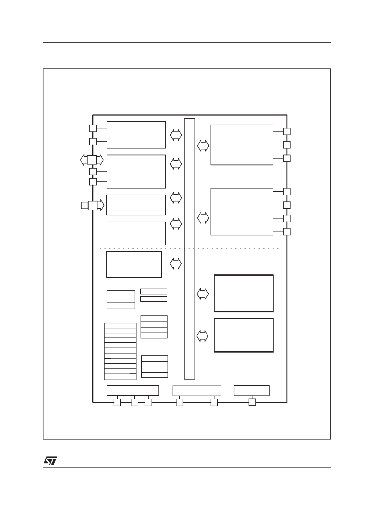
Figure1.ST52x301ArchitecturalBlock Diagram
2/99
ST52T301/E301
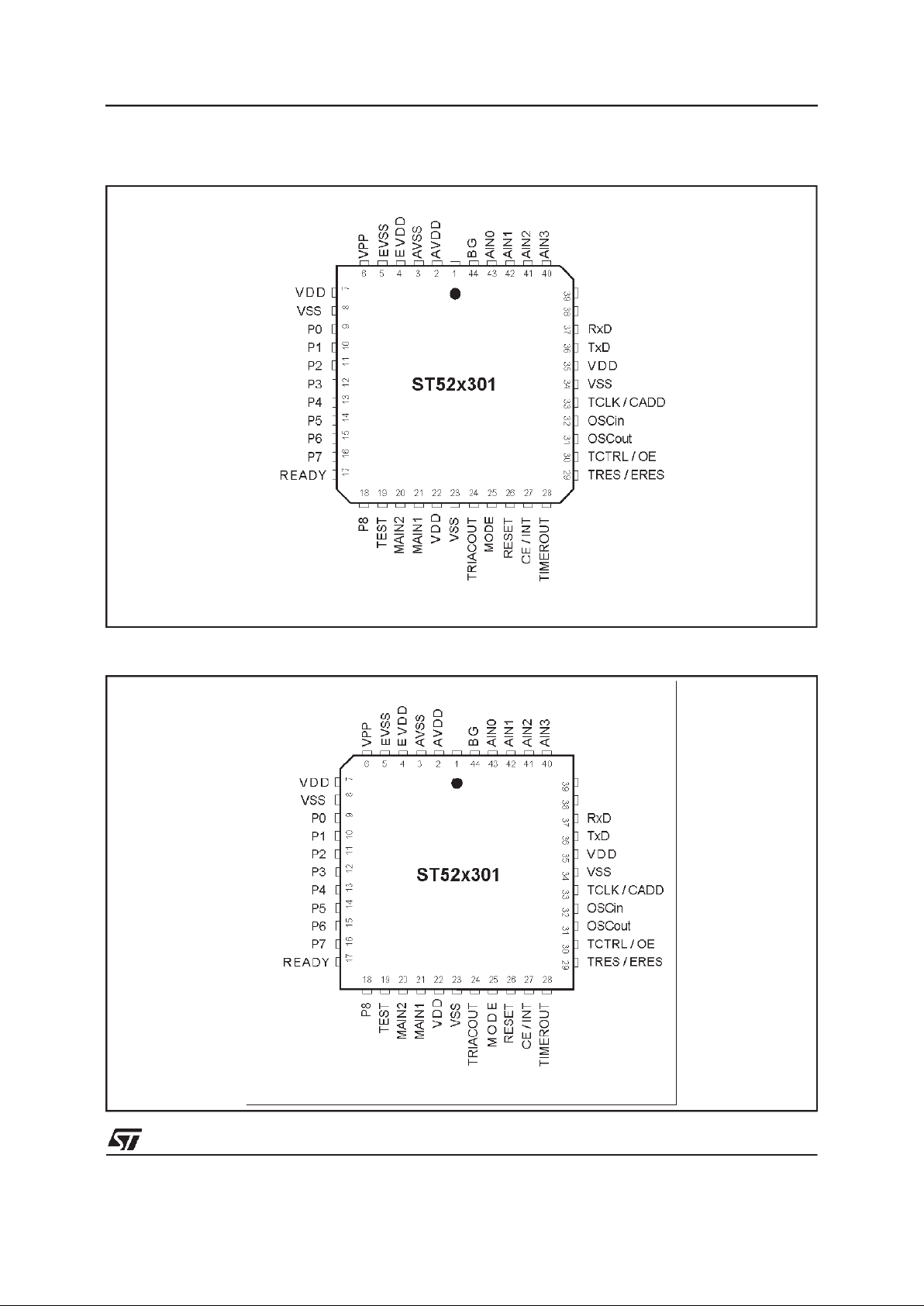
Figure 2.CLCC44-W Pin Configuration
Figure3.PLCC44 Pin Configuration
3/99
ST52T301/E301

PIN NAME TYPE Programming Phase Working Phase
1 not connected - -
2 AV
DD
Analog V
DD
Analog V
DD
3 AV
SS
Analog Ground Analog Ground
4 EV
DD
EPROM Digital Power Supply EPROM Digital PowerSupply
5 EV
SS
EPROM Digital Ground EPROM DigitalGround
6 V
PP
EPROM Programming
Powersupply (12V
±5%)
EPROMV
DD
(5V ±10%)
7 V
DD
Digital Power Supply Digital Power Supply
8 V
SS
Digital Ground Digital Ground
9 P0 I/O I/O EPROM Data Digital I/O
10 P1 I/O I/O EPROM Data Digital I/O
11 P2 I/O I/O EPROM Data Digital I/O
12 P3 I/O I/O EPROM Data Digital I/O
13 P4 I/O I/O EPROM Data Digital I/O
14 P5 I/O I/O EPROM Data Digital I/O
15 P6 I/O I/O EPROM Data Digital I/O
16 P7 I/O I/O EPROM Data Digital I/O
17 READY O I/O port Handshaking Signal
18 P8 O Digital Output
19 TEST I (must be set to 0) (must beset to 0)
20 MAIN2 I/O Zero Crossing/Prescaler Output
21 MAIN1 I Zero Crossing
22 V
DD
Digital Power Supply Digital Power Supply
23 V
SS
Digital Ground Digital Ground
24 TRIACOUT O Triac/PWM DriverOutput Pulses
25 MODE I Functionment Mode Selector Functionment Mode Selector
26 RESET I General Reset General Reset
27 CE/INT I Chip Enable EPROM External Interrupt
28 TIMEROUT O Output Timer
29 ERES / TRES I EPROM Address Counter Reset External TimerReset
30 OE / TCTRL I EPROM OutputEnable Timer Start/Stop Signal
31 OSCout I/O Oscillator Output Oscillator Output
32 OSCin I Oscillator Input Oscillator Input
33 CADD /TCLK I EPROM Change Address Clock Timer External Clock
34 V
SS
Digital Ground Digital Ground
35 V
DD
Digital Power Supply Digital Power Supply
36 TxD O SCI Output
37 RxD I SCI Input
38 not connected - -
39 not connected - -
40 AIN3 Ainp Analog Input
41 AIN2 Ainp Analog Input
42 AIN1 Ainp Analog Input
43 AIN0 Ainp Analog Input
44 BG Aout Band Gap Output
Table1.PLCC44 and CLCC44-WPin Configuration
4/99
ST52T301/E301

1.2 PIN DESCRIPTION
V
DD,EVDD,VSS
,
EV
SS,AVDD
,AV
SS,VPP
.
In order to
avoidnoise disturbances,the power supplyof the
digitalpartis keptseparatedfromthepowersupply
of the analogpart.
V
DD.
MainPowerSupply Voltage(5V 10%).
V
SS
.Digitalcircuit Ground.
EV
DD.
EPROM Main Power Supply Voltage (5V
10%).
EV
SS
.EPROMDigitalcircuit Ground.
AV
DD
. Anal og VDDof the Analog to Digital
Converter.
AV
SS
.AnalogVSSoftheAnalogtoDigitalConverter.
Must be tiedto VSS.
VPP. Main Power Supply for the internal EPROM
(12.5V5%).
OSCin and OSCout. These pins are internally
connected with the on-chip oscillator circuit. A
quartz crystal or a ceramic resonator can be
connectedbetweenthesetwopinsinordertoallow
the correct operations of ST52x301 with various
stability/cost trade-offs. An external clock signal
canbe appliedtoOSCin,in thiscaseOSCoutmust
be grounded.
RESET
.Thissignalis used torestart ST52x301at
thebeginningof itsprogram.Italsoallowsto select
the program mode forthe EPROM.
INT
. External interrupt active on rising or falling
edge.
AIN0-AIN3. These 4 lines are connected to the
inputs of the analog multiplexer. They allow to
acquire4 analoginputs.
BG
.A Voltageequalto 2.5Visavailableonthispin.
It can be used forAnalogsignal conditioning.
P0-P7.These8 lines areorganizedas oneI/Oport.
During the Programmingphase such port is used
forthe EPROM data read/write.
READY.Handshakesignal of the parallelport.
P8.Digital output.
TxD. Serial data output of the SCI transmitter
block.
RxD
. Serial data input of the SCI receiver
block.
TRES,TCLK,TCTRL, TIMEROUT.These pins are
relatedwith the internalProgrammableTimer.The
Timer can be reset externally by using TRES. In
Working Mode, TRES resets the address counter
of the Timer.TRES is active atlowlevel
The Timer Clock can be the internal clock or can
be supplied externally by using the pin TCLK.
AnexternalStart/Stopsignalcanbeusedto control
theTimerthroughthepinTCTRL.TheTimeroutput
is availableon thepin TIMEROUT.
MAIN1,MAIN2,TRIACOUT
. ST52x301 is able to
drive a TRIAC in two different modes:Burst mode
or Phase AnglePartializationcontrolmode.
The Burst mode is usedforthermal regulation.
MAIN1 and MAIN2 signals are used to detect the
zero crossingof the main voltage.
ThepulsetodrivetheTRIACis givenbyTRIACOUT
pin.
It is possible to use the samepins to implement a
PWM Driver. In this case it is possible to fix the
periodof PWMand to changethe dutycycleon fly.
ThePWM output isgiven by TRIACOUT pin.
CE,OE,ERES,CADD,V
PP
. These pins are used
to manage the EPROM during the Programming
phase. During the Programming phase
(programming) V
PP
must be set at 12V. In the
Working phase V
PP
mustbe equalto VDD.
ERES in Programming Mode resets the address
counterof the EPROM;it is active athigh level.
Inthe Workingphase OE,CE andCADDare used
likehandshakingsignalsfor the parallelport.
MODE
. It selects the function ment mo de
(Programmingor Working mode).
TEST.It enablesthe testing functionalities;during
theProgrammingandWorkingphaseitmustbeset
to 0.
5/99
ST52T301/E301
2 INTERNAL ARCHITECTURE
ST52x301is made up by the followingblocksand
peripherals:
Control Unit
Fuzzy Core
ALU
EPROM
Clock Oscillator
Analog Multiplexerand A/D Converter
PrescalerTimer
Bandgap
Triac/ PWMDriver
Digital I/O port
Serial Communication Interface
ST52x301Operating Modes
ST52x301works in twomodes,Programmingand
Working Modes,dependingon the controlsignals
levelRESET, TESTand MODE.
The Operatingmodes are selected by setting the
control signal level as specified in the Control
SignalsSettingtable.
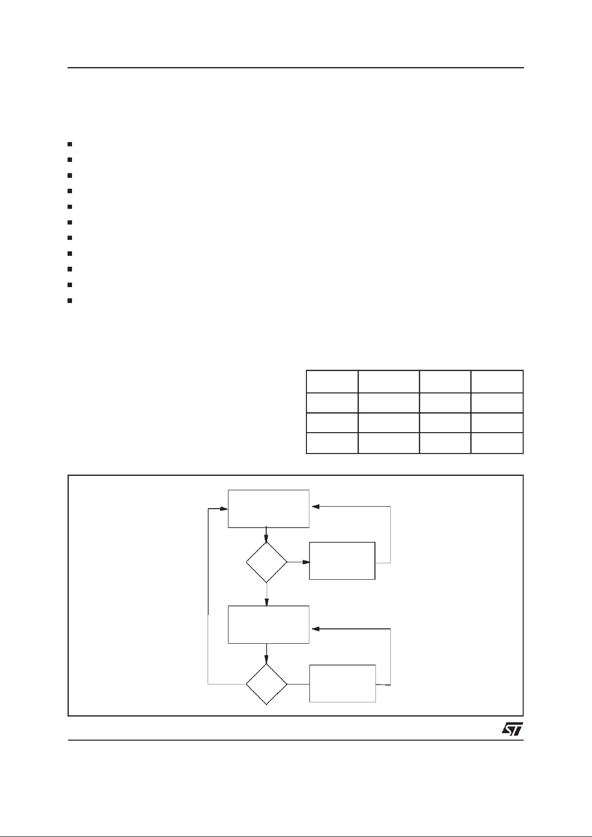
2.1 CONTROL UNIT
The Control Unit (CU) manages: Registers File,
Input Registers, Configuration Registers, ALU,
Accumulatorand Multiplexerinputs.Moreoverthe
CU drives the Fuzzy Core and the peripherals
(Triac/PWM Driver andTimer).
The CU reads the stored instructions on the
EPROM (Fetch) and decodifies them. If the
instructions are arithmetic or logic, the CU runs
them directly, sending the control signals to the
related blocks. If there is a STOP instruction, the
CU transfersthe control to the FuzzyCore.
The Fuzzy Core (FC) will read thenext instruction
(thatmustbeafuzzyinstruction)fromthe EPROM.
The FC mantains the control of the program until
the next STOP instruction. Then the FC transfers
the control to the CU.
Thesecharacteristicsallowto mixfuzzy algorithms
withmathematicaland logic instructions.
Figure2.1 showsa flow-chartreasumingthe logic
behaviourof the instructions management.
Control
Signal
Programming Reset Working
RESET
001
TEST
000
MODE
100
Table2.1.Control Signals setting
CU
Readsfromthe EPROM
and
Decodifies the instruction
CU
executesinstruction
FuzzyCore
Readsfromthe EPROM
and
Decodifies the instruction
STOP?
STOP?
No
No Fuzzy Core
executesinstruction
Yes
Yes
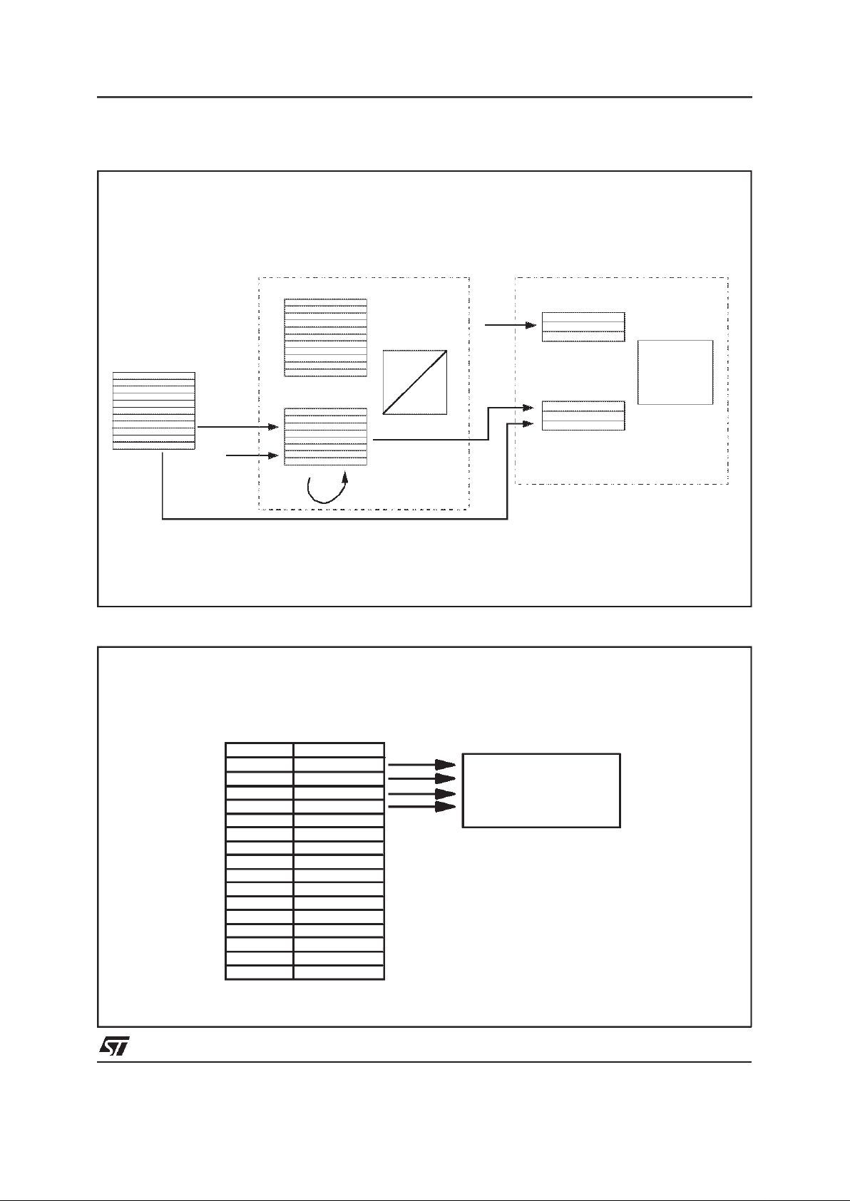
Figure2.1.ComputationAlgorithm FlowChart
6/99
ST52T301/E301
8 BIT
A/D CONVERTER
EPROM
2 KBytes
TIMER
TRES
TCLK
TIMEROUT
FUZZY CORE
I/O
PARALLEL PORT
P0..P7
AIN0..AIN3
POWER SUPPLY
OSCILLATOR
RESET
TRIAC/PWM
DRIVER
MAIN1
MAIN2
TRIACOUT
CONTROL
UNIT
RESETOSCinVSSVDD
ALU
PC
Register File
Input
Registers
INP_PORT
SCI_IN
SCI_ST
FUZZY_OUT_0
FUZZY_OUT_1
ADC_OUT_0
ADC_OUT_1
ADC_OUT_2
ADC_OUT_3
TMR_OUT
TMR_ADC_ST
VPP
Reg 0
Reg 15
Reg 1
REG_CONF0
REG_CONF15
REG_CONF1
Configuration
Registers
SCI
(UART)
TxD
TCTRL
RxD
FLAGS
P8
READY
OSCout
Peripheral
Register
PERIPH_REG_0
PERIPH_REG_1
PERIPH_REG_2
Figure2.2.ST52x301BlockDiagram
7/99
ST52T301/E301

It isnot possibileto stopthe fuzzy inferencebefore
theendof thedefuzzificationof one output.Aset of
26 different arithmetic and logic instructions is
available.Eachinstructionrequiresfrom4 to7clock
pulsesto be performed.
2.1.1 ProgramCounter
TheProgramCounter(PC) is a 11-bit register that
containsthe address of the next memory location
tobe processed bythe core.This memory location
maybe anopcode,an operandoranaddressof an
operand.
The 11-bit length allows the direct addressing
modeof 2048 bytes in the program space.
After having read the current instruction address,
the PC value is incremented. To execute relative
jumpsthe PCand theoffset are shiftedthroughthe
Fuzzy Core or theALU, where they will be added.
The result ofthis operationis shifted backinto the
PC.
The PC can be changedin thefollowing ways:
JP (Jump) instruction PC= JumpAddress
Interrupt PC= InterruptVector
RETI instruction PC =Pop(stack)
Reset PC= Reset Vector
Normal Instruction PC= PC + 1
2.1.2 Flags
TheST52x301coreincludestwopairsof flagsthat
correspondto 2 differentmodes:normal mode and
interruptmode.Each pair consistof a CARRY flag
anda ZEROflag.Onepair (CN,ZN) is usedduring
normal operation and one is used during the
interruptmode (CI,ZI).
The ST52x301 core uses the pair of flags that
correspond to the actual mode: as soon as an
interruptis generated,the ST52x301core usesthe
interruptflagsinsteadof thenormalflags.Whenthe
RETI instruction is executed the normal flags are
restoredif theMCUwas in the normal modebefore
the interrupt. It shouldbe observed that each flag
setcan onlybe addressedin its ownroutine.
The flags are not cleared during the context
switching and remain in the state they were at the
exitof the last routine switching.
The Carry flag is set when a carry or a borrow
occursduring arithmeticoperations,otherwiseit is
cleared.
The switching between the two sets of flags is
automatically performed when an interrupt or a
RETI instructionoccur.
2.2 ADDRESS SPACES
W.A.R.P3TChas four separateaddressspaces:
RegisterFile:16 8-bitregisters
Input Registers:11 8-bit registers
ConfigurationRegisters:16 8-bit registers
PeripheralRegisters:3 8-bit registers
Programmemory up to 2K Bytes
The Program memory will be described in further
detail in the MEMORYsection
2.2.1 Register File
The Register File (RF) consists of 16 general
purpose8-bit registers Reg0 to Reg15.
Allthe registersin theRF can be specifiedby using
a decimal address,
e.g. 0 identify the first register of the RF, called
Reg0.
Reg0:3 are directly connectedto the FC input. It
meansthat the input values of the fuzzyalgorithm
mustbe loadedinto theseregisters bythe user.
These registers are used as temporary registers
duringthe macros’computation.
8/99
ST52T301/E301
Input Registers
ALU
LDRI
Register File
FUZZY
CORE
LDPR
LDRR
LDRC
LDCF
CORE ON-CHIP PERIPHERALS
P e r iph er al Reg ister s
Configuration
Registers
Program Mem ory
PERIPHERAL
BLOCK
LDCFCRi,x
(1)
Figure2.3. AddressSpaces description
RegisterFile
Reg0
Reg1
Reg2
Reg3
Reg4
Reg5
Reg6
Reg7
Reg8
Reg9
Reg10
Reg11
Reg12
Reg13
Reg14
Reg15
FUZZY_IN_0
FUZZY_IN_1
FUZZY_IN_2
FUZZY_IN_3
Free
Free
Free
Free
Free
Free
Free
Free
Free
Free
Fuzzy Core
Register Description
Free
Free
Figure2.4. RegisterFiledescription
9/99
ST52T301/E301
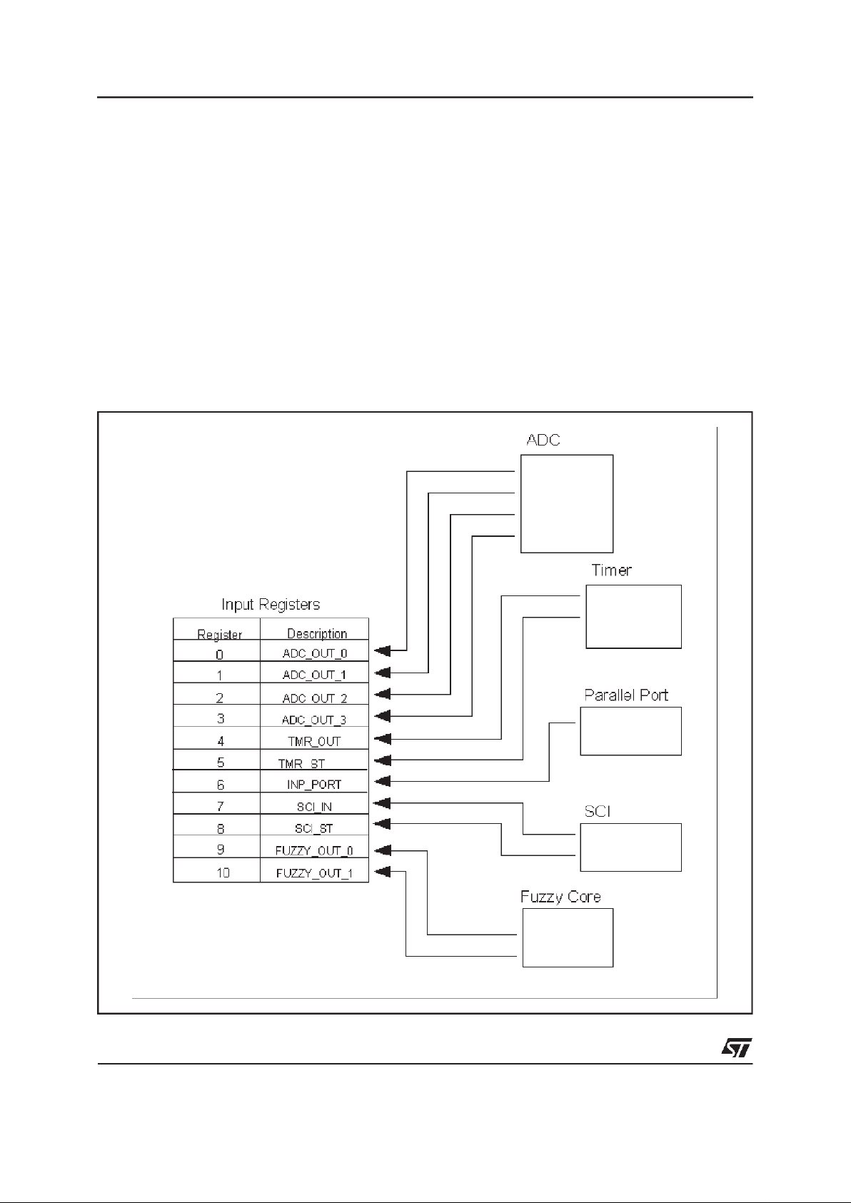
Figure2.5.Input Registers Bench description
2.2.2 Input Registers Bench
TheInput Registers(IR)bench consistsof 118-bit
regis ters co n tai ni ng dat a or statu s of t he
peripherals.
Alltheregisterscanbespecifiedbyusinga decimal
address,e.g.0 identifiesthe firstregister of theIR.
The first four registers (ADC_OUT_0:3) of the IR
are dedicated to the 4 converted values coming
fromthe ADC.
TMR_OUTregisters containsthe current counted
value by the internal Timer; whereas TMR_ST is
the Timer status. For details about TMR_ST,
pleaserefer toTimer description.
Data read by the Parallel I/O Port are stored
automaticallyin the 6-th register, INP_PORT.
Data read by the SCI are stored automatically in
the7-thregisterSCI_IN and SCI status is storedin
the SCI_ST register. For details about SCI_ST,
pleasereferto SCI description.
TheFuzzyCorewritesthe computedoutputvalues
in theFUZZY_OUT_0:1 registers.
10/99
ST52T301/E301
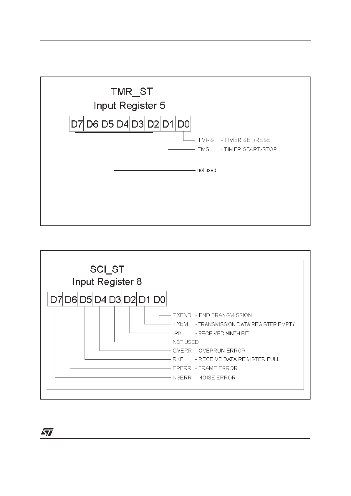
Figure2.6. TMR_ADC_STRegisters
Figure2.7.SCI_STRegisters
11/99
ST52T301/E301

2.2.3 Configuration Registers
The ST52x301 setting permits to configure all
blocks.Table2.2describestherelatedblocktoeach
bit of the ConfigurationRegisters.
Useandmeaningof eachregisterwillbedescribed
in furtherdetails in the corresponding section.
Register Peripheral Bit 7 Bit 6 Bit 5 Bit 4 Bit 3 Bit 2 Bit 1 Bit 0
REG_CONF0
PARALLEL
PORT
IO7 IO6 IO5 IO4 IO3 IO2 IO1 IO0
REG_CONF1
SCI, CORE,
I/O PORT
RDRF OVR BRK TDRE TXC ECKF P8 OUT
REG_CONF2
ADC
not used IADD 1 ADRST
REG_CONF3
SCI
BRSL T8 M RE TE
REG_CONF4
TIMER
TMLSB
REG_CONF5
TIMER
TMMSB
REG_CONF6
TIMER
notused POL TMS CKSL TMEL IESL TMST TMRST
REG_CONF7
TIMER
not used FZSL INPSL INTR INTF INTSL
REG_CONF8
TRIAC
TCLSB
REG_CONF9
TRIAC
TCMSB
REG_CONF10
TRIAC
IOSL PSF CKSL MODE TCST TCRST
REG_CONF11
TRIAC
INTSL TCMSK TCTRS POL
REG_CONF12
TRIAC
FZSL INPSL UTPMSB
REG_CONF13
TRIAC
UTPLSB
REG_CONF14
INTERRUPT
EXTI not used MSKTC MSKTM MSKSCI MSKAD MSKE
REG_CONF15
INTERRUPT
INT4 INT3 INT2 INT1
Table 2.2. ConfigurationRegistersdescription
12/99
ST52T301/E301

2.2.4 PeripheralRegisters
Peripheral Registers contain the initialization
valuesforthe Timer,Triac/PWM DriverandParallel
Port.
The peripheral initialization value is kept from a
location of the Register File, by using a LDPR
instruction , or from FUZZY_OUT_0/1 Input
Register according with the related Configuration
Registers.
Table 2.3 describes therelated peripheral to each
ConfigurationRegister.
Useandmeaningof eachregisterwillbedescribed
in furtherdetails in the corresponding section.
Peripheral Register Peripheral
PERIPH_REG_0
Timer
PERIPH_REG_1
Triac/PWM Driver
PERIPH_REG_2
ParallelPort
Table2.3.Peripheral Register description
13/99
ST52T301/E301
2.4 FUZZY CORE
ST52x301Fuzzy Coremain featuresare:
Up to 4 Inputswith 8-bitresolution
Up to 16 Membership Functions(Mbfs) for each
Input (64 possibleMbfs)
Up to 2 Outputswith 8-bit resolution
Possibility to process fuzzy rules with a max.
numberof 8 antecedents
2.4.1 Internal Structure
The block diagram shown in figure 2.9 describes
thestructureofST52x301FuzzyCore.Inthisfigure
wecandistinguishdifferentfunctionalblocks:Alpha
Calculator, InferenceUnit and Defuzzifier. These
blocks allow to perform a MAMDANI type fuzzy
inferencewith crisp consequents.It is importantto
underline that the fuzzyinferenceis performedby
usingasinputsthe first4 locationsof theRegisters
File.
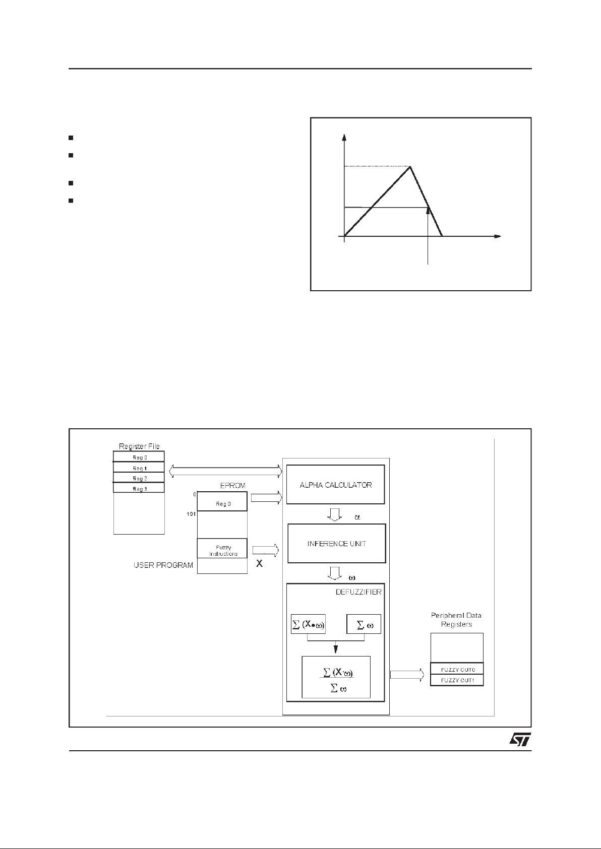
2.4.2 Alpha Calculator Unit
Thisblockperformstheintersection(alpha weight)
betweenthe input values and the relatedMbfs(fig.
2.8).
1
InputValue
α
ij
j-thMbf
i-th INPUT VARIABLE
Figure2.8.Alpha Weigthcalculation
Figure2.9.Fuzzy Core Block Diagram
Notice that the inputs for this blockcome from the
firstfourlocationsof the RegisterFile;it means the
user, to evaluate a fuzzy function, must load the
input valuesin theseregisters.
Alpha Calculator performs what is called
fuzzification
: the input data are transformed in
activationlevel (alpha weight) ofthe Mbfs.
14/99
ST52T301/E301
2.4.3 InferenceUnit
ItmanagesthealphaweightsobtainedbytheAlpha
CalculatorUnit to computethe truth value( ω ) for
each rule.
This is a calculation of the maximum (for the OR
operator) and/or minimum (for the AND operator)
performedon alpha valuesaccordingto the logical
connectivesof fuzzyrules.
It is possibileto linktogetherup to eight conditions
by linguistic connectives AND/OR, NOT operator
and brackets.
Each rule can have at maximum 8 alpha weights
(howevertheyare connected).
The truth value ω and the related output singleton
are passed to the Defuzzifier to complete the
inferencecalculation.
Input 1
X1
α1
Input 2
X2
α2
OR = Max
IF INPUT 1 IS X1 OR INPUT 2 IS X2 THEN.......
Input 1
X1
α1
Input 2
X2
α2
IF INPUT 1 IS X1 AND INPUT 2 IS X2 THEN.......
Figure2.10.
2.4.4 Defuzzifier
This block consists of a Multiplier,two Addersand
one Divider. It generates the output crisp values
implementingthe consequentpart ofthe rules.
In this phase each consequent Singleton X
i
is
multipliedby its weightvaluesω
i
, calculatedbythe
InferenceUnit in order to computethe upper part
of the defuzzification.
Eachoutputvalue(FUZZY_OUT0,FUZZY_OUT1)
is deduced from the consequentcrisp values (X
i
)
by using the defuzzificationformula:
Y
i
=
∑
X
ijωij
j
N
∑
ω
ij
j
N
where:
i = 0,1 identifies the current output variable
N= numberof theactiveruleson thecurrentoutput
ω
ij
=weigthof the j-th singleton
Xij= abscissaof the j-thsingleton
The two fuzzy outputsare stored in the location9
and 10 of the Input Registers (FUZZY_OUT_0,
FUZZY_OUT_1).
1
i-th OUTPUT
VARIABLE
0
X
ij
X
i0
X
in
ω
i0
ω
ij
ω
in
j-th Singleton
Figure 2.11.
15/99
ST52T301/E301

2.4.5 Input Membership Function
ST52x301 allows to manage triangular Mbfs. In
order to definea Mbfit is necessary tostore three
differentdata on thememory:
the vertex of the Mbf: V;
the lenght of the leftsemi-base:LVD;
the lenght of the rightsemi-base:RVD;
In order to reduce the dimension of the memory
area and the computational effort the vertical
dimensionof the vertexis fixed to 15 (4 bits)
By using the previous memorization method it is
possible to store different kinds of triangular
Memberships Functions. In the following figure is
shown a typical example of Mbfs that can be
definedin ST52x301
Each Mbf is then defined storing 3 bytes.To store
all the information related with the fuzzy project
Mbfs, it is necessary to use 192 bytes of the
memory(3 bytes*16Mbfs*4 Inputs = 192bytes).
X
15
LVD RVD
V
15
0
0
InputMbf
OutputSingleton
OutputVariable
InputVariable
w
Figure2.12.MbfsParameters Figure2.13.Exampleof valid Mbfs
The Mbf is memorized by using the following
instruction:
DATAn m lvdv rvd
where
n identifies the input, m identifies the Mbf among
the16 possibleMbfs,lvd,v, rvdare the parameters
describingthe Mbf’s shape.
2.4.6 Output Singleton
ST52x301usesfortheoutputvariablesa particular
kind of membership function called Singleton. A
Singleton has not a shape, like a traditional Mbf,
and it is characterized by a single point identified
by the couple (X, ω), where the ω is calculatedby
the Inference Unit asdescribedbefore.
Oftena Singletonis simply identifiedwith its Crisp
Value X.
16/99
ST52T301/E301

2.4.7 Fuzzy Rules.
The rules can havethe following structures:
if A op B op C...........thenZ
if (A op B)op ( C op D op E...) ...........thenZ
whereop isone of the possiblelinguisticoperators
(AND/OR)
In the first case the rule operators are managed
sequentially;in the second one,the priority of the
operatoris fixed by thebrakets.
Each rule is codifiedby using an istructionset, the
inferencetime for a rule with 4 antecedentsand 1
consequentis about3 microseconds.
TheassemblerInstruction Set allowingto manage
the fuzzy instructions arereported in the following
table:
Instruction Description
DATA n m lvd v rvd Stores the Mbf m of the input n with the shape identified by the parameters lvd, v and rvd.
LDP nm Fixesthe alpha value of the input n with the Mbf m and stores it in the data stack.
LDN n m
Calculates the negatedalpha value of the input n with the Mbf m and store the resultin the data
stack.
FZAND Implements the fuzzy operation AND between the last two values stored in thedata stack.
FZOR Implements the fuzzyoperationOR between the last two values stored inthe data stack.
LDK Stores the result of the lastfuzzy operation executed in thedata stack.
SKM Stores the result of the last fuzzy operationexecutedin the memory register M.
LDM Copies the valueof the register M in the data stack.
CON crisp
Multiplies the crisp valuewith the lastωweight.
OUT n_out Performs the defuzzification.
STOP
Ends the fuzzy algorithm.
Table 2.4. FuzzyInstructions Set
17/99
ST52T301/E301

Example1:
IF Input
1
IS NOTMbf1ANDInput4is Mbf12ORInput3IS Mbf8THENCrisp
1
is codified by the followinginstructions
LDN1 1
calculatesthe NOT α valueof Input
1
withMbf1and stores the resultin the data stack
LDP 4 12
fixesthe α valueof Input
4
withM12and stores the resultin the data stack
FZAND
adds the NOTα andα valuesobtainedwith the operations LDN1 1 andLDP 4 12
LDK stores the resultof the operation FZAND inthe data stack
LDP 3 8
fixesthe α valueof Input
3
withMbf8and stores the resultin thedata stack
FZOR implementsthe operationOR betweenthe resultsobtainedwith the operationsLDK
and LDP
CON crisp
1
multiplies the resultof the lastΩ operationwith the crispvalue Crisp
1
Example2, the priority of the operator is fixedby thebrakets:
IF (Input
3
IS Mbf1ANDInput4IS NOTMbf15) OR(Input1IS Mbf6OR Input6IS NOTMbf14) THEN Crisp
2
LDP 3 1
fixesthe α valueof Input
3
withMbf1and stores the resultin the data stack
LDN4 15
calculatesthe NOT
α valueof Input4withMbf15and stores the resultin the data
stack
FZAND
adds NOT α and α values obtained with the operations LDP 3 1 and LDN4 15
SKM storesthe result of theoperationFZAND in the memory registerM
LDP 1 6
fixesthe α valueof Input
1
withMbf6and stores the resultin the data stack
LDN2 14
calculatesthe NOT
α valueof Input6withMbf14and stores the resultin the data
stack
FZOR
implementsthe operationOR betweenthe α and NOT α valuesobtainedwith the
two previous operations(LDP 1 6 andLDN 2 14)
LDK stores the resultof the operation OR in the data stack
LDM copies the value of the memoryregisterM in the data stack
FZOR implementsthe operationOR betweenthe last two valuesstored in the data stack
(LDK and LDM)
CON crips
2
multiplies the resultof the lastΩ operationwith the crispvalue Crip
2
At theend of thefuzzy rules set a byte,to identify
the output involved in the rules, and the STOP
istructionmustbe inserted.
When the STOP instruction is performed, the
controlof thealgorithmgoes backto the CU.
18/99
ST52T301/E301

2.5 ARITHMETICLOGIC UNIT
The 8-bit Arithmetic Logic Unit (ALU) allows to
perform arithmetic calculations and logic
instructions which can be divided into 4 groups:
Load, Arithmetic, Jump and Program Control
instructions(refer to the ST52x301AssemblerSet
forfurther details).
Load Instructions
Menmonic Instruction Bytes Cycles Z S
LDCF LDCF conf,const 2 6 - -
LDRC LDRC reg, const 2 6 - -
LDRI LDRI reg, inp 2 6 - LDPR LDPR per, reg 1 6 - LDRR LDRR regi, regj 2 6 - -
Arithmetic Instructions
Mnemonic Instruction Bytes Cycles Z S
ADD ADD regi, regj 2 7 I I
AND AND regi, regj 2 7 I SUB SUB regi, regj 2 7 I I
SUBO SUBOregi, regj 2 7 I I
Jump Instructions
Mnemonic Instruction Bytes Cycles Z S
JP JP addr 2 6 - JPNS JPNS addr 2 6 - JPNZ JPNZ addr 2 6 - -
JPS JPS addr 2 6 - JPZ JPZ addr 2 6 - -
SCI Instructions
Mnemonic Instruction Bytes Cycles Z S
SRX SRX regi 2 5 - -
STX STX regi 2 5 - -
Notes:
I affected
- notaffected
Table 2.5. Arithmetic& LogicInstructionsSet
The computational time required for each
instruction consists of one clock pulse for each
Cycleplus 3 clockpulses for the decoding phase.
19/99
ST52T301/E301

Program ControlInstructions
Mnemonic Instruction Bytes Cycles Z S
RETI RETI 1 5 I I
RINT RINT int 1 4 - STOP STOP 1 4 - WAITI WAITI 1 4 - -
UDGI UDGI 1 4 - -
UEGI UEGI 1 4 - -
MDGI MDGI 1 4 - MEGI MEGI 1 4 - -
IRQ IRQ int label 2 6 - -
IRQM IRQM mask 2 6 - -
IRQP IRQP cost 2 6 - -
Notes:
I affected
- notaffected
Table 2.6. Arithmetic& LogicInstructionsSet (Continue)
20/99
ST52T301/E301

3 EPROM
The EPROM memory provides an on-chip
user-programmable non-volatile memory, that
allowsfastand reliable storage of userdata.
Thereare 16K bitsof memory spacewith an 8-bit
internal parallelism (2Kbytes) addressed by an
11-bitbus.The data bus is of 8 bits.
The memory has a doublesupply:V
PP
is equalto
12V±5% in Programming Phase and 5V±10%
duringWorkingPhase.V
DD
is equalto 5V±10%.
The EPROM memory of ST52x301 is divided in
three main blocks (see Figure3.1):
Mbfs Setting with (0 through 191) contains the
coordinatesof the vertexesof everyMbf defined
in theprogram.
Interrupt Vectors (192 through 201) contain the
addressesfor the interruptroutines.
Each address is composedof twobytes.
Program Instruction Set (202 through 2048)
containsthe instructionset of theuser program.
It canbe composed of moreBooleanand Fuzzy
Algorithms
The operation that can be performed, during
Programming Phase,on the EPROMare:Writing,
Verify,Writing Inhibit,Standbyand Erasing.
Figure 3.2 shows the signals timin g in
Programming Mode.
0
192
191
202
201
2048
Mbfs Setting
InterruptVectors
Program
InstructionsSet
Boolean Algorithm
Boolean Algorithm
FuzzyAlgorithm
FuzzyAlgorithm
······
INT_EXT
INT_TRIAC
INT_TIMER
INT_SCI
INT_ADC
Mbf Parameters
Figure3.1.MemoryMap
3.1 EPROM ProgrammingPhase Procedure
Programming mode is selected by applying
12V±5% voltage to the V
PP
pin and set the control
signalas following:
RESET:0, TEST:0, MODE:1.
CADD, ERES, OE and CE are the control signals
used during the Programming Mode. CADD is
activeon edge,the othersare active onlevel(OE,
CE are activelow,ERES is activehigh).
3.1.1EPROMWriting
Whenthe memoryis blank,all thebits are at logic
level”1”.The dataareintroducedby programming
only the zeros in the desired memory location;
however all input data must contain both ”1” and
”0”.
Theonly wayto change ”0” into ”1”is to erase the
whole memory ( by exposure to Ultra Violet light)
and reprogramit.
Thememory is in Writing modewhen:
CE = LOW
OE= HIGH
withstabledata on the databus P(0:7).
The total programming pulse width (CE = 0 V) is,
typically,50 µs (bymeansof 5pulsesof 10µs),but
beforeactivatingsuch pulse,it is suggestedto wait
for at least 2 µs after V
PP
rises at 12 V .After the
disactivationof the pulse it issuggestedto wait for
21/99
ST52T301/E301
at least 2 µs before updating the data and the
address.
The data updating for the next programming is
performed, directly by the user, on the data bus
P(0:7) while the address is incremented through
the pin CADD.
3.1.2EPROMVerify
A Verify mode is available in order to verify the
correctness of the data written. It is possible to
activate the Verify mode immediately after the
writing of eachbyte:
CE = HIGH
OE= LOW
Then, ifany error in writing occured, the user has
to repeat the EPROMwriting.
The data, during this phase, are avalaible on the
busP(0:7)
3.1.3WritingInhibit
It occursbetween the Writing and Verify Mode:
CE = HIGH
OE= HIGH
3.1.4 Standby Mode
The EPROM has a standby mode which reduces
theactivecurrentfrom10mA(Programmingmode)
to less than 100 µA. The Memory is placed in
standbymode by setting CE at HIGH Logic Level
(V
PP
might be equal to 5 V too).When in standby
mode,the outputs are in highimpedancestate.
3.2 Eprom Erasure
Thanks to the transparent window present in the
CLCC44-Wpackage,its memory contentsmaybe
erasedby exposureto UV light.
Erasurebeginswhenthedeviceisexposed to light
witha wavelengthshorterthan4000Å.It shouldbe
noted that sunlight, as well as some types of
art ificia l light, includes wavelength s in the
3000-4000Årange which, onprolongedexposure,
can cause erasure of memory contents.It is thus
recommended that EPROM devices be fitted with
an opaquelabel over the window area in orderto
preventunintentionalerasure.
Therecommendederasure procedureforEPROM
devicesconsistsof exposureto shortwaveUVlight
having a wavelength of 2537Å. The minimum
recommende d integrat ed dose (intens ity x
expo-su re time) f or co mplete erasure is
15Wsec/cm2 .
This is equivalent to an erasure time of 15-20
minutesusing a UV source having an intensityof
12mW/cm 2 at a distance of 25mm (1 inch) from
the device window.
OE
P(0:7)
DATA IN
VPP
5V
12V
CE
Inhibit
min 2us
2us typ.
DATA OUT
RESET
CADD
Writing Verify
ERES
INPUT
PORT
50us typ.
OUTPUT
PORT
3us min.
Figure3.2.EPROMProgrammingTiming
22/99
ST52T301/E301

4 INTERRUPTS
The Control Unit (CU) responds to peripheral
events and external events through its interrupt
channels.
Whensuch an eventoccurs,if itisnot maskedand
according to a priority order, the current program
execution can be suspended to allow the CU to
executea specificresponseroutine.
Eachinterruptisassociatedwithaninterruptvector
that contains the memory address of the related
interrupt service routine.Each vector is located in
the Program Space (EPROM Memory) at a fixed
address(seeInterrupt Vectorstable fig.4.2).
4.1 Interrupt Functionment
If, at the end of an arithmetic or logic instruction,
there are pending interrupts, the one with the
highest priority is passed. To pass an interrupt
meansto storethe arithmeticflagsand the current
PC in the stack and execute the associated
Interrupt routine, whose address is located in one
of theEPROMmemory location betweenaddress
192 and 201.
TheInterruptroutineisperformedasanormalcode
checking,at theendof eachinstruction,if a higher
priority interrupt has to be passed. An Interrupt
request with the higher priority stops the lower
priority Interrupt. The Program Counter and the
arithmeticflags are storedin the stack.
With the instruction RETI (Return from Interrupt)
thearithmeticflagsand ProgramCounter(PC)are
restoredfrom the topof thestack.Thisstack,used
forthe Interrupt priority, is a LIFOqueue.
AnInterruptrequest cannotstop the processingof
the fuzzy rules but this is passed only after the
definitionof thefuzzyoutputorattheendof a logic
or arithmetic instruction.
4.2 Global InterruptRequestEnabling
When an Interrupt occurs, it generates a Global
InterruptPending(GIP), that can be hangedup by
software.After a GIP a Global Interrupt Request
(GIR) will be generate and Interrupt Service
Routine associated to the interrupt with higher
prioritywill start.
In order to avoid possible conflicts between
interruptmaskingset inthemainprogramor inside
macros, the GIP is hanged up through the User
GlobalInterrupMask or the MacroGlobalInterrup
Mask (see fig.4.3).
UEGI/UDGI instruction switches on/off the User
GlobalInterrupMaskenabling/disablingtheGIRfor
the main program.
MEGI/MDGI instructions set the Macro Global
InterruptMaskinorder toassurethatthe macrowill
not be broken.
NORMAL
PROGRAM
FLOW
INTERRUPT
SERVICE
ROUTINE
RETI
INSTRUCTION
INTERRUPT
Figure4.1.Interrupt Flow
InterruptVectorsINT_TIMER
198
196
200
199
197
195
194
193
192
191
INT_SCI
INT_ADC
INT_TRIAC
INT_EXT
202
201
Figure4.2.Interrupt VectorsMapping
Global Interrupt
Pending
User Global
InterruptMask
Macro Global
InterruptMask
Global Interrupt
Request
Figure4.3.Global Interrupt Request generation
23/99
ST52T301/E301

4.3 Interrupt Sources
ST52x301managesinterruptsignalsgeneratedby
the internal peripherals (Timer, Triac/PWM
Driver,Analog to Digital Converter and Serial
CommunicationPort) orcomingfrom the INT pin.
The polarity of the External Interrupt is
programmedby the EXTIbit of theREG_CONF14
(see Table 4.1 and fig. 4.4). EXTI=0 means that
INT_EXT is active on rising edge, otherwise it is
activeon fallingedge.
Each peripheral can be programmed in order to
generatethe associateinterrupt;furtherdetailsare
describedin therelatedchapter.
4.4 Interrupt Maskability
The interrupts can be masked by configuring the
REG_CONF14.The interruptis enabledwhen the
bit associated to the mask interrupt i s ”1”.
Viceversa, when the bit is ”0”, the interrupt is
maskedand is keptpendent.
ForexampleLDCF 14, 6
(CONF_REG14 =00000110) enables interrupts
comingfromtheADC(INT_ADC)and fromtheSCI
(INT_SCI).
4.5 Interrupt Priority
Six priority levels are available: level 5 has the
lowestpriority,level0 hasthe highestpriority.
Level5 isassociatedtothe MainProgram,levels4
to 1 are programmable by means of the priority
register called RE G_CONF15 (see fig.4.5);
whereas the higher levelis related to the external
interrupt(INT_EXT).
Timer, Triac/PWM Driver, SCI and ADC are
identifiedby a twobitsPeripheralCode (see Table
4.2); in order to set the
i
-th priority level the user
must write the peripheral label
i
in therelatedINT
i
prioritylevel.
Bit Name Value Description
0 MSKE
0
External Interrupt
Masked
1
External Interrupt
Not Masked
1 MSKAD
0
A/D ConverterInterrupt
Masked
1
A/D ConverterInterrupt
Not Masked
2 MSKSCI
0
SCI Interrupt
Masked
1
SCI Interrupt
Not Masked
3 MSKTM
0
TIMER Interrupt
Masked
1
TIMER Interrupt
Not Masked
4 MSKTC
0
TRIAC/ PWM Interrupt
Masked
1
TRIAC/ PWM Interrupt
Not Masked
5 not used 6 not used -
7 EXTI
0
Activeon Rising Edge
1
Activeon Falling Edge
Table4.1.ConfigurationRegister 14 Description
Name Description Priority
Peripheral
Code
Maskable
EPROM
Locations
INT_EXT ExternalInterrupt (INT)
Ext Highest - yes 200-201
INT_ADC ADC
Int Programmable 00 yes 192-193
INT_SCI SCI
Int Programmable 01 yes 194-195
INT_TIMER TIMER
Int Programmable 10 yes 196-197
INT_TRIAC TRIAC
Int Programmable 11 yes 198-199
Table 4.2. InterruptsDescription
24/99
ST52T301/E301

D7
D6 D5 D4 D3 D2 D1 D0
REG_CONF14
Interrupt
MSKE - ExternalInterrupt Mask
MSKAD - ADC Interrupt Mask
EXTI - ExternalInterrupt Polarity
MSKSCI - SCIInterrupt Mask
MSKTM - TIMERInterrupt Mask
not used
not used
MSKTC - TRIACInterruptMask
Figure4.4.InterruptConfigurationRegister14
D7
D6 D5 D4 D3 D2 D1 D0
REG_CONF15
Interrupt
INT1 - HIGH Level Interrupt
INT2 - MEDIUM-HIGH Level Interrupt
INT3 - MEDIUM-LOW Level Interrupt
INT4 - LOW Level Interrupt
Figure4.5.InterruptConfigurationRegister15
25/99
ST52T301/E301
i.e. LDCF 15, 201 (REG_CONF15=11001001)
definethe followingpriority levels:
Level1: INT_SCI(SCICode: 01)
Level2: INT_TIMER(TIMER Code:10)
Level3: INT_ADC(ADCCode:00)
Level4: INT_TRIAC(TRIACCode: 11)
Whena sourceprovidesan Interruptrequest,and
the request processing is also enabled, the CU
changes the normal sequentialflow of a program
bytransferingprogramcontrol toa selectedservice
routine.
Whenan interruptoccurs theCUexecutesa JUMP
instruction to the address loaded in the related
locationof the InterruptVector
Whentheexecutionreturnstotheoriginalprogram,
it begins immediately following the interrupted
instruction.
4.6 Interrupt RESET
An eventuallypending interruptscan be resetwith
the instruction RINT int
i
which resets thei-th
interrupt
Bit Name Value Level
0, 1 INT1
Peripheral
Code
High
2, 3 INT2
Peripheral
Code
Medium-High
4, 5 INT3
Peripheral
Code
Medium-Low
6, 7 INT4
Peripheral
Code
Low
Table4.3.ConfigurationRegister 15 Description
Figure4.6.Exampleof a Sequenceof InterruptRequests
26/99
ST52T301/E301
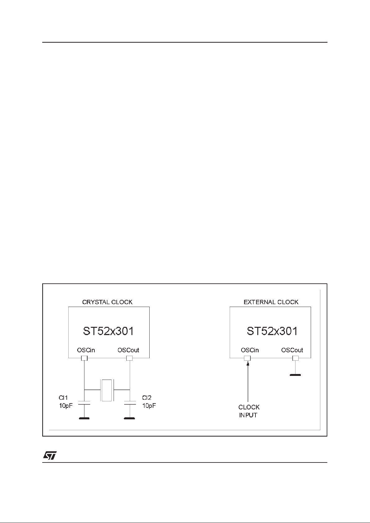
5 CLOCK
ST52x301 can work by using a 5, 10 or 20 MHz
clock.
TheST52x301 ClockGeneratormodule generates
theinternalclock for theinternal ControlUnit,ALU,
Fuzzy Core and on-chip peripherals and it is
designed to require a minimum of external
components.
Thesystemclockmaybegeneratedbyusingeither
a quartz crystal, or a ceramic resonat or
(CERALOC);or, at least, by means of an external
clock.
The different clock generator options connection
methodsare shown inFigure 5.1.
When an external clock is used, it must be
connectedonthepinOSCinwhileOSCoutmustbe
grounded.
The crystal oscillator start-uptime is a function of
manyvariables:crystalparameters(especiallyR
S
),
oscillator load capacitance (CL), IC parameters,
ambienttemperature,supplyvoltage.
It must be observed that the crystal or ceramic
leads and circuit connectionsmust be as short as
possible.Typical values for CL1, CL2are 10pF for
a 20MHzcrystal.
Figure5.1.OscillatorConnections
27/99
ST52T301/E301
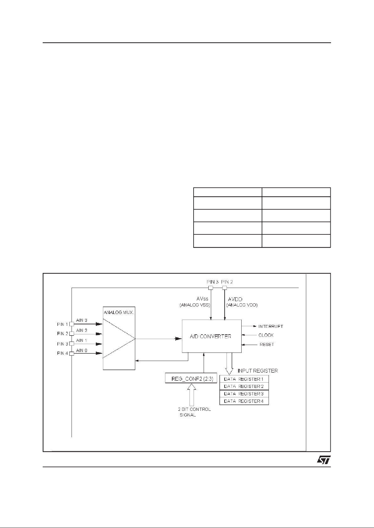
6. A/D CONVERTER
TheA/D Converter ofST52x301is an8-bitanalog
to digital converter with up to 4 analog inputs
offering8 bit resolution with a total accuracy of 2
LSB and a typical conversiontime of 32 µs.
Theconversionrange is 0 - 2.5V.
TheA/D peripheralconverts theinputvoltagewith
a process of successive approximations using a
fixedclock frequencyderived fromthe oscillator.
The ADC uses 5 registers: one Configuration
Register, REG_CONF2, and four Data Registers.
These4 registersare the first4 InputRegisters.
The A/D converterdrives theanalogMultiplexerin
order to sequentiallypickup the external inputs to
be put in output and storedautomaticallyin 4 8-bit
registers.
ItispossibiletoconfiguretheMultiplexerbymeans
of the registerREG_CONF2,in orderto select the
numberof analoginputs to convert.
Forexample,if thebit 3 andbit 2 of REG_CONF2
are configured at 10, then the Multiplexer will
sequentiallypickup only theinputs 0,1 and 2.
Table 6.1 shows the convertion sequences
according to the possible values of the two bit
REG_CONF2(3:2).
The A/D Converter,at the end of the conversion,
willsend a signal(end-of-conversion)whichcanbe
used like an interrupt signal. The user can select
the priority of the A/D interrupt and mask it (see
”InterruptRoutine”chapter)
The conversion start s writing ”1” on
REG_CONF2(0).The A/Dis resetby writing ”0” in
REG_CONF2(0).
Theconverteddataare automaticallystoredin four
8-bit Input Registers.
By performingan instruction:
LDRI regj ingi
theanaloginput”ingi”is loadedintheregister”regj”
of the RegisterFile.
Figure6.1.A/D Converter Structure
CONF_REG2 (3:2) INPUT SEQUENCE
00
Ain0
01
Ain 0, Ain1
10
Ain 0, Ain1, Ain 2
11
Ain 0, Ain1, Ain 2, Ain 3
Table6.1.
28/99
ST52T301/E301

The power consumption of the device can be
reducedby turning off the A/Dconverter,
ToswitchofftheA/DconvertertheCONF_REG2(0)
bit must bereset to ”0”.
The A/D Converter features a sampleand hold.
The input voltage Ain, which has to be converted
must be constant,for 12.8 µs.
An internal bandgap reference is available on pin
44, BG. By using this signal as reference for the
signalto be converted,theconversionaccuracy is
not strongly related withthe variation of the power
supply.
The power supplyof the A/D converter (AV
DD
and
AV
SS
) in orderto avoidinterferencesis mantained
separatedfromthe powersupplyof thedigitalcore.
D7 D6 D5D4 D3 D2D1 D0
ADC
Configuration Register
REG_CONF2
Reset ADC
Must be1
ADC inputselection
Not used
Figure6.2.ConfigurationRegister REG_CONF2
29/99
ST52T301/E301

7.TIMER
ST52x301 offers one on-chip Timer peripheral.
TheTimerconsists of an 8-bit counterwith a 16-bit
programmable prescaler, thus giving a maximum
count of 2
24
, an d c ontrol logic that allows
configuring the functionment and the type of
peripheral outputs. Figure 7.2 shows the Timer
block diagram and Figure 7.3 shows the internal
structureof the Timer.
Thecontentof the 8-bitcountercanberead/written
andis incrementedon the RisingEdge of the16-bit
prescaleroutput(PRESCOUT).Moreover,itcan be
read under program control at any instant of the
counting phase and loaded in a location of the
RegisterFile.Theprescalercanbe givenanyvalue
between 0 and FFFFh setting the 4-th (TMLSB)
and 5-th (TMMSB) locations of the Configuration
RegistersBench.
7.1TimerFunctionment
TheTimer requires three signals:TMRCLK,TRST
andTSTART(seeFigure7.3).Eachofthemcanbe
generatedinternallyor externally,this possibility is
programmableby the user.
TMRCLK increments the counted value of the
Pre sc a ler. It can be, by se tt in g C KSL of
REG_CONF6 register, the internal clock signal
(CLKM)or the signalprovidedon the pinTCLK.
TRSTresetsto zerothe contentofthe8bit counter.
It is generated by the TRES or RESET external
signalsoritisforcedbyTMRSTbitofREG_CONF6
register.
TSTARTstarts/stopsthePrescalercounting.It can
be given on the pin TCTRL orit isforcedby TMST
bit of REG_CONF6register.
The TSTART signalallows to work in two different
modes:
LEVEL (Time Counter)
: If the TSTART signal is
hightheTimerstarts thecount.WhentheTSTART
islow the count is stoppedand thecurrent valueis
stored in the TMR_OUT register of the Input
registerBench,thenit can betransferredtothe j-th
location of the Registers File by using the
instruction:
LDRI reg-j 4
EDGE(Period Counter)
: Afterthe reset,when the
firstedge oftheTSTARTsignalappears,theTimer
starts the count,at the next TSTART the Timer is
stopped.In this way it is possible to measure the
periodof an external signal.
The functionment modality is set by the TMEL
configurationbit of REG_CONF6register.
The starting value of the Counter can be either a
value contained in the Register File or directly a
FuzzyOutput.If INPSL(REG_CONF7(3))is set to
”1”thenthe value comes from oneof the locations
of the Register File (LDRP 0, reg-i); on the
contrary it is generated by the Fuzzy Core. The
choice between the two possible fuzzy outputs is
set by the FZSL configurationbit of REG_CONF6
register
FZSL=0/1 means the starting value is the loaded
fromthe FUZZY_OUT_0/1.
Level
Edge
start stop
start
start
stop
start
00 033321
Reset
Clock
Counted
Value
Figure7.1.Timer Functionalities
30/99
ST52T301/E301

Figure7.2.Timer PeripheralBlockDiagram
31/99
ST52T301/E301

Figure7.3.Timer Internal Structure
32/99
ST52T301/E301

7.2TimerInterrupt
It is possible to enable the Timer Interrupt by
softwarecontrol.TheTimercanbeprogrammedto
generate an Interrupt request until the end of the
count or when there isan externalTSTARTsignal.
The Timer can generateprogrammableInterrupts
in to4 differentmodes:
Interrupt mode 1
: Interrupt oncounterStop.
Interrupt mode 2
: Interrupt on Rising Edge of
TIMEROUT.
Interrupt mode 3
: Interrupt on Falling Edge of
TIMEROUT.
Interrupt mode 4
: Interrupt on both edges of
TIMEROUT.
InordertoprogramtheinterruptmodeINTSL,INTF
and INTR bits of the REG_CONF7 must be set
following theindicationsshownintheTable7.1.The
Timer interruptcan be used to exitthe MCU from
theWAITmode.
7.3TimerConfiguration
TheTimerconfigurationneeds to set 4registersof
the ConfigurationRegister Bench.
CONF_REG4:
TMLSB contains the less significative bits of the
Prescalerstarting value.
CONF_REG5:
TMMSB containsthe moresignificativebits of the
Prescalerstarting value
Timer Output
Type1
Type2
Prescout*Counter
Figure7.4.TIMEROUTSignalType
INTERRUPT
MODE
INTSL INTF INTR
11XX
2 010
3 001
4 011
Table7.1.Timer InterruptSetting
D7
D6
D5 D4 D3 D2 D1 D0
REG_CONF4
Timer
TMLSB - PrescalerInit Value
Less Significative Bits
D7
D6
D5 D4 D3 D2 D1 D0
REG_CONF5
Timer
TMMSB - PrescalerInit Value
More Significative Bits
Figure7.5.Timer ConfigurationRegister4 and 5
33/99
ST52T301/E301

D7
D6
D5 D4 D3 D2 D1 D0
REG_CONF6
Timer
TMRST - InternalTimer Reset
TMST - Internal Timer Start
not used
IESL - Internal/External Signals Selector
TMEL - Edge/Level Timer Abilitation
TMS - Timer Output Shape
POL - TimerOutput Polarity
CKSL - Internal/External Clock Select
Figure7.6.Timer ConfigurationRegister6
Bit Name Value Description
0 TMRST
0
Stop
1
Start
1 TMST
0
Stop
1
Start
2 IESL
0
Internal Signals
1
External Signals
3 TMEL
0
on Edge
1
on Level
4 CKSL
0
Internal TimerClock
1
External TimerClock
5TMS
0
Pulse Wave(Type2)
1
Square Wave (Type 1)
6 POL
0
Positive Polarity
1
Negative Polarity
7
not
used
-
Table7.2.ConfigurationRegister 6 Description
CONF_REG6:
TMRST sets the internal INR signal.
TMST sets the internalINS signal.
IESL selects the source of the TRES and
TSTARTsignals.
IESL=”0”signalsaretheinternalINRand
INS.
IESL=”1” signals come from the TRES
and TCTRL pins.
TMEL selects the TSTART signal allowing to
workinLevelMode orinEdge Modelike
previouslydescribed.
TMEL=”0”means Edge Mode
TMEL=”1”means LevelMode.
CKSL selectsthesourceoftheTMRCLK(work-
ing Timer frequency).
CKSL=”0”, the TMRCLK is the internal
MCLK divided by the Prescaler starting
value.
CKSL=”1”, the TMRCLK is an external
clockbyTCLK pin.
TMS TIMEROUT is a signal with frequency
equal to the working Timer frequency
dividedby the starting value of thePrescaler (16 bit) and Counter (8 bit). The
Timeroutputcan be eithera squarewave
with duty-cycle 50% or a pulse signal
(withthepulsedurationequaltothePrescaler output signal period).
TMS=”1”, TIMEROUT is a squarewave
TMS=”0”, TIMEROUTis a pulse signal.
POL defines the polarity of the Timer output
signal(TIMEROUT).
34/99
ST52T301/E301

Bit Name Value Description
0 INTSL
0
INT_TMR on FallingEdge of
Counter Stop
1
INT_TMR on Edges of
TIMEROUT
1 INTF
0
NO INT_TMR on Falling
Edge of TIMEROUT
1
INT_TMR on FallingEdge of
TIMEROUT
2 INTR
0
NO INT_TMR on Rising
Edge of TIMEROUT
1
INT_TMR on Rising Edge of
TIMEROUT
3 INPSL
0
Timer Data Input coming
from theFuzzy Core
1
Timer Data Input coming
from aRegister File location
4 FZSL
0
Timer Data Input coming
from FUZZY_OUT_0
1
Timer Data Input coming
from FUZZY_OUT_1
5 not used 6 not used 7 not used -
Table7.3.ConfigurationRegister 7 Description
D7
D6 D5 D4 D3 D2 D1 D0
REG_CONF7
Timer
INTSL - Interrupt GeneratorSelector
INTF - Interrupton TIMEROUTFallingEdge
INTR - Interrupton TIMEROUTRising Edge
INPSL - InputData Selector
FZSL - Fuzzy InputSelector
not used
not used
not used
Figure7.7.Timer ConfigurationRegister7
CONF_REG7:
INTSL It allows to selectthe interrupt mode for
the Timer.
INTSL=”0”Interrupt is generated on the
fallingedge of the Counter Stop.
INTSL=”1”the interrupt is generatedon
the edges of TIMEROUT.
INTF
INTR
INPSL selects the source of the value of the
CounterbetweenalocationoftheRegister Fileand the Fuzzy Core.
INPSL=”0”, Counter value coming from
the FC.
INPSL=”1”, Counter value coming from
the RF.
FZSL
FZSL=”0”,thevalueoftheTimerCounter
is equalto FUZZY_OUT_0
FZSL=”1”,thevalueoftheTimerCounter
is equalto FUZZY_OUT_1
35/99
ST52T301/E301

8 I/OPORT
ST52x301 is provided with dedicated lines for
input/output.These lines,groupedintoan 8-bit I/O
PortP(0:7),canbe programmedtoprovideparallel
input/output with a handshake line (READY) to
carry data in/out.
The I/O Port is not able to perform operationson
the single bit, and the communication cannot be
performedat the sametime in inputand output.
It is possible to programthe parallel port direction
by usingthe register REG_CONF0 in order to set
which bits are in inputand which are in output.
The port has an i nternal register
(PERIPH_REG_2) dedicated to hold output data
coming from the Register File through an LDPR
instruction.
InputdataareautomaticallystoredintheIN_PORT
register, 6-thlocation of the Input Register.
P8 pin is a digital output line available directly
connected to the OUT bit of the REG_CONF1;
thenit can be set by using a LDCFinstruction.
(seetable 8.2and Figure 8.8)
PERIPH_REG_2(i)
P(0:7)
I/O PIN
TTL
CMOS
IO(i)
INP_PORT(i)
TRISTATE
REG_CONF0(i)
P8
OUTPUTPIN
REG_CONF1(0)
OUT
Figure 8.1.
Figure8.2.
36/99
ST52T301/E301

8.1 I/O PORTCONFIGURATION
REG_CONF0 allows dynamic change in I/O Port
configurationduringprogramexecutionsetting the
communicationdirectionof each bit.
IOi
settingequal to ”0”configures the i-thbit
of theP(0:7) I/O Port ininput.Data coming from external digital devices are
storedin the 6-thlocation(INP_PORT)of
the Inputregister bench.
IOi=”1” sets the i-th bit of the port in
output.Data stored in the i-th locationof
the Register File iswritten on theport by
using the instruction:
LDPR 2, regi
Bit Name Value Description
0 IO0
0
Input Pin
1
Output Pin
1 IO1
0
Input Pin
1
Output Pin
2 IO2
0
Input Pin
1
Output Pin
3 IO3
0
Input Pin
1
Output Pin
4 IO4
0
Input Pin
1
Output Pin
5 IO5
0
Input Pin
1
Output Pin
6 IO6
0
Input Pin
1
Output Pin
7 IO7
0
Input Pin
1
Output Pin
Table8.1.ConfigurationRegister 0 Setting
D7
D6
D5
D4 D3 D2 D1 D0
REG_CONF0
I/O Port
IO0 - I/OCommunication Direction Bit
IO1 - I/OCommunication Direction Bit
IO2 - I/OCommunication Direction Bit
IO3 - I/O Communication Direction Bit
IO4 - I/O Communication Direction Bit
IO5 - I/O Communication Direction Bit
IO6 - I/O Communication Direction Bit
IO7 - I/O Communication Direction Bit
Figure8.3.ConfigurationRegister 0
37/99
ST52T301/E301

8.2 INPUT HANDSHAKE
Figure8.5 illustrates the timingassociatedwith the
READY Handshake signal, when the instruction
LDRI reg 6 is performed.
Whenthe LDRIinstruction is executedto readthe
port, ST52x301 resets the READY signal to
indicate that it is not possibleto change the input
dataduring this phase of reading.
TosynchronizethetransmissionwithREADYsignal
will prevent the INP_PORT data from changing
whileST52x301is readingthe port.
READPORTsignal representedin figure8.5 is an
ST52x301internal signal.
Input data on the port are continuously sampled
and are strobedinto theport only when READY is
set.
W.A.R.P.3TC
xxxxxx0x
REG_CONF1
P(7:0)
IOP
EXTERNAL
PERIPHERAL
DATA
READY
I/O
PORT
Figure 8.4.One Line Input Handshake
PIO(7:0)
READY
DATAIN
READPORT
CLK
NEWDATA IN
Figure8.5.One LineInput HandshakeTiming
38/99
ST52T301/E301

8.3 OUTPUT HANDSHAKE
Figure8.7 illustrates the timingassociatedwith the
READY Handshake signal, when the instruction
LDPR 2 reg is performed.
WhenREADYisresetno significantdataare onthe
output port pins,because ST52x301 is writinginto
the PERIPH_REG_2.
When the data is ready in PERIPH_REG_2,
READY signal is set.
Therisingedgeof READYsignalcan beusedas a
latchingsignal.
No peripheralacknowledgeis waited for.
If thesignal READY is high, it means thatthe data
outisstillnot read.Inthiscase,the followingLDPR
instruction is stored in a one register peripheral
stack.
If the READY is maintained high, the following
LDPR instructions store the data coming fromthe
RegistersFile on thesame register stack.
Figure8.6.One Line Output Handshake
Figure8.7.One LineOutput Handshake Timing
39/99
ST52T301/E301

ItmeansthateachLDPRinstructiondeletestheold
value contained in the parallel port stack register
andrewritea newvalueonthesamestackregister.
Only the last LDPR instruction is executed if the
READY signal is maintained high during several
LDRP instructions.
Bit Name Value Description
0P8 -
Digital Output Bit
1
ECKF
00
5 MHz
01
10 MHz
2
10
20 MHz
11
20 MHz
3 TXC
0
SCI EndTransmission
Interrupt Disabled
1
SCI EndTransmission
Interrupt Enabled
4 TDRE
0
SCI TransmissionData
Register Empty Interrupt
Disabled
1
SCI TransmissionData
Register Empty Interrupt
Enabled
5 BRK
0
SCI BreakError Interrupt
Disabled
1
SCI BreakError Interrupt
Enabled
6 OVR
0
SCI OverrunError Interrupt
Disabled
1
SCI OverrunError Interrupt
Enabled
7 RDRF
0
SCI ReceivedData Register
Full Interrupt Disabled
1
SCI ReceivedData Register
FullInterrupt Enabled
Table8.2 ConfigurationRegister 1 Setting
Figure8.8.
40/99
ST52T301/E301

9 SERIALCOMMUNICATION INTERFACE
The Serial Communicat ion Inte rface (SCI)
integrated into the fuzzy processor ST52x301
provides a gene ral purpose shift register
peripheral, that allows to link several widely
distributed MCUs, through their SCI subsystem.
The S CI gives a serial interfa ce providing
communication with common baud rates, up to
38400Hz, andflexible character format.
The SCI is a full-duplexUART-type asynchronous
system with standard Non Return to Zero (NRZ)
format for the transmitted/receivedbit. The length
ofthe transmittedword is 10/11 bits(1 startbit,8/9
databits, 1 stop bit).
The SCI is composedof threemodules:Receiver,
Transmitter and Baud-Rate Generator and it is
configuredby means of ConfigurationRegisters 3
and 1.
9.1 SCI RECEIVERBLOCK
The SCI Receiver block manages the
synchronization of the serial data stream and
stores the data characters. The SCI Receiver is
mainly formed by two sub-systems: Recovery
BufferBlock andSCDR_RXBlock.
The RE configurationbit set to ”1” (Configuration
Register3) enablesthe SCI Receiver.
The SCI receives data coming from the RxD pin
and drives the Recovery Buffer Block, that is a
high-speed shift register operating at a clock
frequency(CLOCK_RX) 16 times higher than the
fixed baud rate (CLOCK_TX).This sampling rate,
higher than the Baud Rate clock, allows to detect
Figure 9.1.SCI transmittedwordstructures
Figure9.2.SCI Block Diagram
41/99
ST52T301/E301

Bit Name Value Description
0TE
0
Transmission DISABLED
1
Transmission ENABLED
1RE
0
Receiver DISABLED
1
Receiver ENABLED
2
M
00
8, No Parity,1 bit stop
01
8, No Parity,2 bit stop
3
10
8, Parity,1 bit stop
11
9, No Parity,1 bit stop
4T8
0
Parity Odd, if Parity is
selected (M
= 10); otherwise
9th Data bit
1
Parity Even, ifParityis
selected (M = 10);otherwise
9th Data bit
5
BRSL
000
600 Hz
001
1200 Hz
010
2400 Hz
6
011
4800 Hz
100
9600 Hz
101
19200 Hz
7
110
38400 Hz
111
External Clock
Table9.1 ConfigurationRegister3 Setting
theSTARTcondition,theNoiseerrorand theFrame
error.
When the SCI Receiver is in IDLE status, it is
waiting for the START condition, that is obtained
with a logic level 0, consecutiveto a logic level 1.
Thisconditionisdetected,if,withthefixedsampling
time, three logic levels 0 are sampled after three
logic levels1.
The recognition of the START bit forces the SCI
Receiver Block to enter in an data acquisition
sequence,according to serial mode.
The2 bits,M, ofthe ConfigurationRegister3 allow
todefinetheserialmodewith theconventionshown
in table9.2.
Thebit,T8,incaseofM
=
10
isused to setthe parity
checkto perform,as indicatedin the previoustable
9.2.
The recognition of STOP condition allows to
transferthe receiveddata, from Recovery Bufferto
SCDR_RX buffer, adding the eventual ninth data
bit,accordingto themeaningshownintheprevious
table 9.2. After this operation, RXF flag of SCI
StatusInputRegister 8 (fig.9.3) is set tologiclevel
1.The ControlUnit readsthe datafrom SCDR_RX
buffer (in read-only mode) with SRX instruction
and providesa resetat logic level0 to RDRF flag.
If a data of Recovery Buffer is ready to be
transferredinto SCDR_RX buffer,but the previous
one was not yet read by the Core, an OVERRUN
Errortakesplace:the status flag OVERRindicates
the error condition. In this case the information
stored in SCDR_RX buffer is not altered, but the
one that has caused the OVERRUN error can be
overwrittenby a new data coming from the serial
dataline.
RecoveryBuffer Block
This block is structured as a synchronised finite
state machine on the CLOCK_RX signal falling
edge.
Whenthe RecoveryBufferBlockis in IDLEstate it
waits for the reception of the correct 1 and 0
sequencerepresentingthe START.
The recognition takesplace by samplingthe input
RxD at CLOCK_RX frequency, that has a
frequency 16 times higher than CLOCK_TX. For
this reason, whilethe externaltransmittersends a
single bit, the Recovery Buffer Block samples 16
states(fromSAMPLE1to SAMPLE16).
42/99
ST52T301/E301

Bit Name Value Description
0P8 -
Digital Output Bit
1
ECKF
00
5 MHz
01
10 MHz
2
10
20 MHz
11
20 MHz
3 TXC
0
SCI EndTransmission
Interrupt Disabled
1
SCI EndTransmission
Interrupt Enabled
4 TDRE
0
SCI TransmissionData
Register Empty Interrupt
Disabled
1
SCI TransmissionData
Register Empty Interrupt
Enabled
5 BRK
0
SCI Break Error Interrupt
Disabled
1
SCI Break Error Interrupt
Enabled
6 OVR
0
SCI Overrun Error Interrupt
Disabled
1
SCI Overrun Error Interrupt
Enabled
7 RDRF
0
SCI Received Data Register
Full Interrupt Disabled
1
SCI Received Data Register
FullInterrupt Enabled
Table9.2 ConfigurationRegister 1 Setting
The analysis of RxD input signal is carried out
lookingthree samples for each bits received.0
Ifthesethreesamplesarenotequal,thenthenoise
error flag, NSERR, of Input Register 8 is set to 1
and the received data value will be the one
assumedby the majority of the samples.
By means of the procedure described above, to
avoid SCI becomes IDLE, because of a limited
noise due to an erroneous sampling, the
transmissionisrecognizedascorrectandthenoise
flagerror is set.
At the end of thecycle relativeto the receptionof
a bit, Recovery Buffer Block will repeat the same
steps 9 times:one step for each receivedbit, plus
oneforthestopacquisition(10timesin caseof 9-bit
data,double stop or parity check).
Attheendofdatareception,RecoveryBufferBlock,
will supply informationon eventualframeerrors by
settingto 1 FRERR flag bit ofInput Register 8.
A frame error can occur if the paritycheck has not
been successfully achievedor if STOPbit has not
beendetected.
If Recovery Buffer Block receives 10 consecutive
bits at logic level 0, a break error occurres, and
interruptroutine request starts.
SCDR_RX block
It is a finite state machine synchronized with the
fallingedgeof the clock master signal, CKM.
The SCDR_RX block waits the signalof complete
reception, from the Recovery Buffer, to load the
word received. Moreover, the SCDR_RCX block
loads the values of FRERR and NSERR flag bits
(InputRegister 8), and sets theRXF flag to 1.
Using SRX instruction the data are transferredto
RegisterFile andRXF flag is resetto 0, toindicate
SCDR_RX blockis empty.
If a new data arrives before the previous one has
been transferredto RegisterFile, an overrunerror
occurres and OVERRflag, of Input Register 8, is
setto 1.
43/99
ST52T301/E301

9.2SCI TRANSMITTER BLOCK
TheSCI TransmitterBlockconsistsof thefollowing
underblocks: SCDR_TX and SHIFT REGISTER,
synchronized, respectively, with the clock master
signal(CKM) and theCLOCK_TX.
The whole block receives through Configuration
Register 3 (M bits) the settings for the following
transmissionmodes (see table9.1):
8-bit wordanda singlestop signal
8-bitwordplus a paritybit andasinglestop signal
8-bit wordplusa doublestop signal
9-bit word
In case of 9 bit frame transmission, the most
significative bit arrives through T8 of the
ConfigurationRegister 3.
In an 8-bit transmission, instead, T8 is used to
configure the SCI, according to information
containedinM (seetable9.1):in particularto chose
thepolaritycontrol(evenor odds)toimplementthe
paritycheck.
Aftera RESETsignal,RST, the SCDR_TXblock is
inIDLEstateuntil it receivesenablingsignal,TE=1,
of ConfigurationRegister 3.
If TE=1, using STX instruction the data, to be
transmitted, are transferred from Register File to
SCDR_TX block and the flag of Input Register 8,
TXEM,is resetto 0, toindicate SCDR_TXblockis
full.
If the core supplies a new data, this could not be
loadedinthe SCDR_TXblockuntilthe currentdata
hasnot beenunloaded on the Shift Registerblock.
Thismeansthatonlywhen TXEMis 1,itispossible
to load data in the SCDR_TX Block.
Whenthe SHIFT REGISTERBlockloads thedata
to be transmitted on an internal buffer,TXEND is
reset to 0 to indicate the beginning of a new
transmission.Atthe endoftransmission TXENDis
setto 1, allowing to load in the SHIFT REGISTER
a newdata comingfrom SCDR_TX.
It is important to underline that TXEND = 1 does
notmeanSCDR_TXis readyto receiveanewdata.
Forthisreasonit is bettertoutilisethe TXEMsignal
to synchronize the STX instruction to the SCI
TRANSMITTER block
If ST52x301core resets TE to 0, the transmission
is interrupted, but the SCI Transmitter block
completes the transmission in progress before to
reset.
9.3 Baud Rate GeneratorBlock
The Baud Rate Generator Block performs the
divisionof the clock master signal (CKM), in a set
of synchronism frequencies for the serial bit
reception/transmissionon theexternal line.
Table9.1.shows the setof frequenciesselected by
meansof BRSL (ConfigurationRegister 3).
Reception frequency (CLOCK_RX) is 16 times
higherthan transmissionfrequency(CLOCK_TX).
If BRSL is equal to 111, CLOCK_RX and
CLOCK_TX signals coincide with clock master,
CKM.
Figure9.3.SCI Status InputRegister
44/99
ST52T301/E301

10TRIAC/PWMDRIVER
ST52x301 offers a peripheral able to generate a
signal on pin 24, TRIACOUT, to drive an external
device, like a TRIAC, a IGBT or a Power Mos.
Triac/PWM driver can perform 3 different working
modes according to REG_CONF10 bits, MODE
(seeTable10.4):
MODE= ”01”: PWM
MODE= ”10”: Burst Mode Triac Control
(ThermalRegulations)
Note:in this case CKSL of REG_CONF10must
be set to”1x”.(see Table10.4)
MODE= ”11”:
Phase Angle Partialization
TriacControl (MotorControl)
TheTriac/PWMDrivercan beinitializedbyusing a
valuefixedbya controlalgorithm,thatcanbe either
the output of a fuzzy inference or the result of an
arithmeticcalculus stored in theRegisterFile.
In the latter case, by using the LDPR 1,reg-i
instruction,the value,containedin the i-th register
of RegisterFile, is storedin the Triac Driver/PWM
peripheralregisterPERIPH_REG_1.
Figure 10.1 shows the internal structure o f
Triac/PWMDriver.
PWMMode
The PWM working mode is obtained by setting
REG_CONF10bits, MODE, at ”01”value.
Itconsistsof a signal,withfixedperiod, whoseduty
cyclecan bemodified.
Figure10.1.TRIAC/PWMDriver Simplified BlockDiagram
45/99
ST52T301/E301

D7 D6 D5D4 D3 D2 D1 D0
REG_CONF8
TRIAC / PWM
TCLSB - Prescaler init value
Least SignificativeBits
D7 D6 D5 D4 D3 D2 D1 D0
REG_CONF9
TRIAC / PWM
TCMSB - Prescaler init value
Most SignificativeBits
Figure10.2.TRIAC/PWMConfigurationRegister 8 and 9
The PWM period can be generated, internally, by
dividingthe masterclockor,externally,by using an
externalclock signal.
Inboth cases,theclocksignalis dividedby a 16-bit
Prescaler, managed by REG_CONF8 and
REG_CONF9(see Figure10.2).
Thedutycycleis fixedby a value,thatcanbeeither
the output of a fuzzyinference or the result of an
arithmetic calculus. In the first case, it can be
loaded directly in the register of the peripheral,
otherwise it can be stored in one location of the
Register File for further manipulations and then
used for the controlof thePWM.
BurstMode
It is based on turning on and off the TRIAC,for a
fixed integer number of main voltage periods, in
order to controlthe power transferredto the load.
For this reason a Burst Mode TRIAC control
consistsof a signal,with a period, T,containingan
integernumberofthe main voltageperiods,whose
duty cycle is proportionalto the numberof periods
inwhichthe TRIACis ON(Duty Cycle).Thiskindof
Triac control is mainly usedfor thermal regulation.
Thedutycycleisfixedbya valuethatcanbedirectly
the output of a fuzzyinference or the result of an
arithmeticcalculus.
In order to work in Burstmode, it is necessary to
detect the pre-post zero-crossingof main voltage,
by using an externalinserting circuitry.
Theuser can define the period T, by means of the
internal 16-bit prescaler, setting REG_CONF8 and
REG_CONF9 (seeFigure10.2).T isproportionalto
the main voltage period,it is in the range 0 to 21.8
sec(if themainfrequencyis 50Hz).
The width and the polarity of the pulses can be
programmedaccording to the Triac andthe circuit
characteristics.
PhaseAngle PartializationMode
Thismethodis basedon turningontheTRIAConly
for a part (phase angle) of each main voltage
period.When the phase angle is large the energy
(power)suppliedto the loadis low,viceversa,when
thephaseangleis smallthe energy suppliedto the
load is high.
Thephaseangle can befixedbya fuzzyalgorithm
or by a value stored inthe RegisterFile.
Thephase angle is an 8-bit value.
The peripheral is programmable in order to work
witha mainvoltagefrequencyof 50or 60 Hz.
46/99
ST52T301/E301

10.1PWMGENERATOR WORKINGMODE
When REG_CONF10 (3:2) bits, MODE, are ”01”,
the peripheral is programmed to work in PWM
Mode.
Byusingthe 16-bitprescaler,the PWMperiod can
begeneratedbydividingthe internal masterclock,
or an external clock signal applied on the pin
MAIN1,or themainvoltagefrequency,by usingthe
circuitshownin Figure 10.6.
NOTE: The external clock signal, applied on
MAIN1pin,musthavea frequencyat leastthree
timesmaller than the internal master clock.
The clock source can be selected by using
REG_CONF10(5:4)bits,CKSL(seeTable10.4and
Figure10.9).If theclocksourceselectedis notthe
mainvoltagefrequency(CKSL=1x),MAIN2pincan
be configure d as input or o utput, by using
REG_CONF10(7)bit, IOSL (see Table10.4).
If MAIN2 is an output, on this pin it is possible to
get the prescaleroutput signal Tck.
Theperiod of the PWMsignalis obtainedby using
the followingrelation:
T=256*Tck
where Tck is the output of the 16-bit prescaler
managedbyREG_CONF8and REG_CONF9(see
Figure10.2).
NOTE. In PWM working mode, the value N,
stored in the 16-bit prescaler, must be in the
range from 2 to 2
16
-1
By using a 20 MHz clock master it is possible to
obtain a PWM frequency in the range 1.2 Hz to
26.04KHz.
The value Ton is proportional to a value,
INIT_VALUE,that can be a fuzzy output or a value
Value Description
01
PWM Driver
10
Burst Mode Control
(1)
11
Phase Angle Control
Note:
(1)
REG_CONF10(5) must be set to ”1”
Table10.1.MODE - Triac/PWMWorkingMode
Settings
MCLK
Frequency
1/T
min max
5 MHz 0.3Hz 6.51 kHz
10 MHz 0.6 Hz 13.02 kHz
20 MHz 1.2 Hz 26.04 kHz
Table10.2.PWM Frequencies
T=256*Tck
Ton= INIT_VALUE*Tck
Toff
TRIACOUT
Figure10.3.PWMFunctionament
coming from Register File, according with the
INPSL and FZSL configuration bits of
REG_CONF12(see Table10.6 andFigure 10.12).
TheTon isequal to:
Ton=INIT_VALUE*Tck.
It means the Ton can be fixed by the control
algorithm that can be either the output of a fuzzy
inferenceor the resultof an arithmeticcalculus.In
thesecondcase,the data,storedinthei-thlocation
of the Register File, can be loaded by using the
instruction:
LDPR 1, reg-i.
If the INIT_VALUEis 255the Toffis equaltoTck.
47/99
ST52T301/E301

10.2BURSTMODE
When REG_CONF10 (3:2) bits, MODE, are ”10”
the peripheral is programmed to work in BURST
MODE.
Notice that when you are working in Burst mode
CKSL must be set to ”1x”
.(see Table10.4)
A squarewave, Tb, is generated with a dutycycle
proportional to the power the user intends to
transferon the load. A pulseis generatedfor each
zero crossing of the main voltage included in the
Ton of the fixed period. Figure 10.4 shows the
typicalBurstControlworkingmode.TheperiodTof
thesignalTb (seeFigure10.4)is equalto 256*Tck.
ThesignalTckisgeneratedprogrammingthe16-bit
Prescaler, by REG_CONF8 and REG_CONF9
(seeFigure 10.2).Tck is equalto themain voltage
frequency(50 or 60 Hz) divided by N+1,where N
valueis from0 to 2
16
-1.
The value Ton is proportional to a value,
INIT_VALUE,that can be a fuzzy output or a value
coming from Register File, according with the
INPSL and FZSL configuration bits of
REG_CONF12(see Table 10.6 andFigure10.12).
On TRIACOUT pin is generated a sequence of
pulses, programmed, by using REG_CONF11(0)
bit,POL (see Table 10.5), inorderto be positiveor
negative, to drive the Triac in different quadrants.
The number ofgeneratedpulses, N_PULSES, is:
N_PULSES= 2 [(N+1)*INIT_VALUE- N]
whereN is the valuestoredin the16-bit pescaler.
ThenTon = (N_PULSES/ 2)* T
POWER LINE
The first pulse is obtained during the first zero
crossing of the main voltage and the last one is
generated after INIT_VALUE*Tck clock pulses,
where Tck is the Prescaler output, generated by
usingthe mainvoltagefrequencyappliedto MAIN1
and MAIN2 pins.
Theperipheralcanbeprogrammed inordertowork
with50 or60Hz mainvoltagefrequency,by setting
theREG_CONF10(6)bit, PSF(seeTable 10.4).
Ranges of the Tb signal period depend on the
powerline frequency(see Table10.3).
Inorder to drive a Triac in BurstModeit is required
to generate a sequence of pulse, that must be
centred on the zero crossing of the power line as
shownin the Figure 10.7. For this reason,the pre
zero crossing and the post zero crossing of the
powerline must be detected.
To detect the zero-crossing andget also the main
voltagefrequency, the user must generateMAIN1
and MAIN2 signals, by using the circuit shown in
Figure10.6.
MAIN1 and MAIN2 signals are used in the block
calledPULSEGENERATORof theperipheral(see
Figure10.1).
Inparticular the pulsesare generatedbyusing the
riseedge of the signal MAIN1 and the falling edge
of the signalMAIN2.
Figure 10.5 shows the generation of the Triac
pulsesTp.
The first firing pulse for the Triac is generated on
the zero crossing of the powerline, whilethe next
pulsesare centred on the zerocrossing.
Power Line
Frequency
T
min max
50 Hz 5.12 s 335544 s
60 Hz 4.26 s 279620 s
Table10.3.TRIACOUTSignal Period
-1.5
-1
-0.5
0
0.5
1
1.5
Ton
Tb
Power
Line
TRIACOUT
T = 256 * Tck
Figure10.4.BurstWorkingMode
48/99
ST52T301/E301

Normallythe Triacfiring pulsesstart 1/3 Tp before
thezerocrossingand thelengthof thepulsesisTp,
seeFigure 10.5.
The length Tp of the pulses is programmable by
usingUTP value,that is a14-bitsnumber,obtained
with REG_CONF12(5:0) bits, UTPMSB, and
REG_CONF13, UTPLSB (see figure 10.12 and
table10.6):
UTP(13:0)= [UTPMSB(5:0)UTPLSB(7:0)]
T
P=TMCLK
* UTP
The value Tp is in therange 0 to 4.9 ms whenthe
clockmaster is 20MHz.
According to REG_CONF11(0) configuration
register bit, POL, it is possible to set the firing
(1)
(0.5)
0
0.5
1
Ig
Tp
Negative
Triac Gate
Current
2/3 Tp
Tp
1/3 Tp
Positive
Triac Gate
Current
Power
Line
Ig
II and III quadrants
I and IV quadrants
Figure10.5.Burst Mode pulse polarity
Figure10.6 BurstMode ZeroCrossingCircuit
MAIN1
MAIN2
-1.5
-1
-0.5
0
0.5
1
1.5
MainVoltage
TRIACOUT
Tp Tp TpT
MASK
T
MASK
Figure10.7 BurstMode Zero Crossing
MCLK
Frequency
T
P
min max
5 MHz 0.0012 ms 19.6608 ms
10 MHz 0.0006 ms 9.8304 ms
20 MHz 0.0003 ms 4.9152 ms
pulses polarity; in order to obtain positive or
negative gate Triac currents, allowing to work
respectively in I and IV quadrants,or in the II and
III quadrants (see Figures10.5and 10.12).
To increase the immunity of the peripheralagainst
the el ectrical n oise of the main voltage, a
prog rammable masking time, by usin g
REG_CONF11(5:2)bits, TCMSK (see Table10.5)
49/99
ST52T301/E301

and Figure 10.11), is introduced after each firing
pulse (see Figure 10.7):
Maskingtime =(2^TCMSK*200+100) nS.
If TCMSK is 0 then Maskingtime is 0.
In fact, to avoid the detection of electrical noise,
during the masking time no signal, coming from
MAIN1and MAIN2, istaken into account.
Working in the II and III quadrant the peripheral
implementsthe followingprocedure:
1) Thefiring pulseis set to ”1”on therisingedgeof
MAIN1.
2) The firing pulse is resetto ”0” after the time Tp
fixedby program.
3) The firing pulseis resetto ”0”for a timeequal to
the fixed masking time.
4) Onthe falling edge of MAIN2the firing pulseis
setto ”1”
5) The firing pulse is resetto ”0” after the time Tp
fixedby program.
6) The firing pulseis resetto ”0”for a timeequalto
the fixed masking time.
Following this approach it is possible to filter
electrical noise and oscillations on the signal
MAIN1and MAIN2.
It ispossibleto generatea programmableInterrupt
in four differentways:
1) No Interrupt;
2) Interrupt onthe rising edgeof the signal Tb.
3) Interrupt onthe falling edge of the signalTb.
4) Interrupt onboth the edgeof the signal Tb.
TheInterruptis programmablebyusingtheregister
REG_CONF11(7:6),INTSL (seeTable10.5).
(1.5)
(1)
(0.5)
0
0.5
1
1.5
(1.5)
(1)
(0.5)
0
0.5
1
1.5
V
A2-A1
Il
180 360
00
α
γ
Phase Angle
Current Flow Angle
L
N
Load
A2
A1
Il
Figure10.8.PhaseAngle PartializationMode
10.3 PHASE ANGLE PARTIALIZATION WORKINGMODE
When REG_CONF10 (3:2) bits, MODE, are ”11”
the peripheral is programmed to work in PHASE
ANGLEPARTIALIZATIONmode.
In this mode Triac is controlledeach period of the
main voltage.The power transferredto the load is
proportional to the CURRENT FLOW ANGLE γ.
ThiskindofTriac controlissuitabletodrivetheTriac
TCMSK MaskingTime
0000
0
µs
0001
0.5
µs
0010
0.9
µs
0011
1.7
µs
0100
3.3
µs
0101
6.5
µs
0110
12.9
µs
0111
25.7
µs
1000
51.3
µs
1001
102.5
µs
1010
204.9
µs
1011
409.7
µs
1100
819.3
µs
1101
1638.9
µs
1110
3276.9
µs
1111
6553.7
µs
50/99
ST52T301/E301

with inductive load (i.e. universal or monophase
motors). In the figure 10.8 is shown the relation
between the Phase Angle α and the Current flow
angle
γ . Theperipheral allowsto controlthe Phase
AngleorequivalentlythetimeT1(seeFigure10.9).
ItispossibletochangeTimeT1settingthecontents
of the peripheral register PERIPH_REG_1. This
value could be directly loaded by using one of the
twofuzzy outputsor byusing a valuecoming from
theRegistersFile, accordingwithINPSLandFZSL
configurationbitsofREG_CONF12(seeTable10.6
and Figure 10.13).
Inorderto synchronizethe peripheralwiththe zero
crossing of the main voltage the two pins MAIN1
and MAIN2 must be connected together if
the
externalcircuitistheoneshownintheFigure10.10.
It is possible to use different circuits for the zero
crossing detection, but the MAIN1 signal rising
edge must be synchronized with a main voltage
zero crossing and the MAIN2 signal falling edge
(1.5)
(1)
(0.5)
0
0.5
1
1.5
Mains
Voltage
10 mS 20 mSec
T1
T1
Tmax
8mS
Tr
Tr/2
Ti
Figure10.9 PhaseAnglePartializationmode
Figure10.10 Phase Angle PartializationZeroCrossing
must be synchronized with the following main
voltagezero crossing, always.
Theperipheralcanbeprogrammedinordertowork
with50 or60 Hzmain voltagefrequencyby setting
theREG_CONF10(6)bit, PSF(seeTable 10.4).
Ifmainvoltagefrequencyis equalto50 Hz, thenTr,
seefigure 10.9, is equal to 20 mSecand T1 is:
T1 = PERIPH_REG_1(0:7)*(1/25.5)ms.
Thelength ofthesemiperiodTi/2 isprogrammable
by using the registers REG_CONF12(0:5) and
REG_CONF13,(seefigure10.12).Byusinga clock
master equal to 20 MHz the pulse width is in the
range from 0.2 to 250 µs. The duty cycle of Ti is
always50 %.
Inorder toavoidproblemsfor the Triacfiringwhen
the load is inductive 8 different pulses are
generatedby the peripheral.
If the timeT1 is bigger thana fixedtime Tmaxthen
nopulsesaregeneratedand theTriacismaintained
off.This featurewasimplementedin orderto avoid
the firing of the Triac in the second half period of
the main voltage. The firing pulses are generated
when the contents of the PERIPH_REG_1 is less
or equal to 204, otherwise they are not generated.
Whenthe frequency of the mainvoltage is 50 Hz,
T1maxis equalto 8 mSec.
It is possibleto generatea programmableinterrupt
in four differentways:
1) no Interrupt;
2) Interrupt on the rising edge of the signalMAIN1
3)Interrupton the falling edgeof thesignal MAIN2
4)Interrupton boththe edgesof the signalMAIN1.
TheInterruptis programmablebyusing the register
REG_CONF11(7:6),INTSL
10.4.TRIAC/PWM DRIVER PROGRAMMING
51/99
ST52T301/E301

Bit Name Value Description
0 TCRST
0
TriacReset
1
TriacSet
1 TCST
0
TriacStop
1
TriacStart
2
MODE
00
not used
01
PWM signal Generator
3
10
Burst Mode
(1)
11
Phase Partialization
4
CKSL
00
Clock Master
01
External Clock on MAIN1
51x
Main VoltageFrequency
6 PSF
0
Main Powerat 50 Hz
1
Main Powerat 60 Hz
7 IOSL
0
MAIN2 Input pin
1
MAIN2 Output pin
Note:
(1)
CKSLmust be set to ”1x”
Table 10.4 Configuration Register 10 Description
Bit Name Value Description
0 POL
0
Output pulse Polarity =
positive
1
Output pulse Polarity =
negative
1 TCTRS
0
TRIACOUT status = Tristate
1
TRIACOUT status = Enabled
2
TCMSK
Masking time
=(2^TCMSK*200 +100) nS.
TCMSK=0→Masking time=0
3
4
5
6
INTSL
00
No Interrupt source selected
01
Interrupt on falling edge of
the TRIAC/PWMsignal, or of
the MainVoltage
7
10
Interrupt on risingedge of
the TRIAC/PWMsignal, or of
the MainVoltage
11
Interrupt on both of edges of
the TRIAC/PWMsigna,l or of
the MainVoltage
Table10.5 Configuration Register 11 Description
Bit Name Value Description
0 ÷ 5
UTPMSB
Output Impulse Width most
significative bits
6 INPSL
0
TRIAC/PWM Input from
Fuzzy Output
1
TRIAC/PWM Input from
Register File
7 FZSL
0
TRIAC/PWM Input from
Fuzzy Output 1
1
TRIAC/PWM Input from
Fuzzy Output 2
Table10.6.ConfigurationRegister 12 Description
It is possible SET or RESET the TRIAC/PWM
Peripheral by using the REG_CONF10(0) bit,
TCRST(seeTable 10.4).
If TRIAC/PWM Peripheral is SET, It is possible
STARTor STOP it, byusing the REG_CONF10(1)
bit, TCST (see Table 10.4), to start or stop the
internal counter without resetting it.
Itis possibletoenabletheTRIACOUT, byusingthe
REG_CONF11(0)bit, TCTRS (seeTable10.5 and
Figure10.11).
IFTCTRSis 0theTRIAC/PWM Peripheraloutput
is in tristatestatus.
52/99
ST52T301/E301

Figure10.11.TRIAC/PWMConfigurationRegister10
Figure10.12 TRIAC/PWMConfiguration Register 11
Figure10.13 TRIAC/PWMConfiguration Registers12 and13
53/99
ST52T301/E301

Symbol Parameter Value Unit
V
DD
SupplyVoltage
-0.5 to 7 V
V
I
Input Voltage
V
SS
-0.3 to VDD+0.3
(1)
V
V
O
Output Voltage
V
SS
-0.3 to VDD+0.3
(1)
V
V
DDA,VSSA
Analog SupplyVoltage
V
SS
-0.3 to VDD+0.3
(1)
V
V
PP
EPROM Programming Voltage
13 V
I
O
Standard Output Source Sink Current
(2)
±
20
mA
TRIACOUT Output Source Sink Current
±80
(3)
mA
T
OPT
Operating Temperature
0 to +85 °C
T
STG
Storage Temperature
-65 to +150 °C
Table 11.1.AbsoluteMaximumRatings
Note: Stresses above those listedinthe Table”Absolute Maximum Ratings” may cause permanent damage to the device.
These are stress ratings only and operation of the device at these or any other conditions above thoseindicated in the Operating
sections of this specificationis not implied. Exposure toAbsolute MaximumRating conditions for extended periods may affect
device reliability.Refer also to the SGS-THOMSON SURE Program and other relevantquality documents.
1.Withinthese limits, clamping diodes are garanteed to be not conductive.
2. All except TRIACOUT pin
3.For not more than 1 sec.
11 ELECTRICAL CHARACTERISTICS
AbsoluteMaximumRatings
Thisproductcontainsdevicesto protecttheinputs
against damage due to high static voltages,
howeverit is advisedto takenormal precautionto
avoid any voltage higher than maximum rated
voltagees.
Forproperoperationit is recommendedthatV
I
and
V
O
mustbe higher than VSSand smallerthan VDD.
Reliability is enhanced if unu sed inp uts are
connectedto an appropriatedlogic voltagelevel
54/99
ST52T301/E301

(
VSS or VDD)RECOMMENDED OPERATING CONDITIONS
(OperatingCondition:V
DD
=5V±5%-TA=0 °Cto85°C,unless otherwise specified)
Symbol Parameters Test Conditions Min Typ Max Unit
V
DD
Operating Supply Voltage
4.75 5.0 5.25 V
V
PP
Programming Voltage
11.4 12 12.6 V
V
O
Ouput Voltage
V
SS
VDD V
V
DDA,VSSA
Analog SupplyVoltage
Vss ≤ V
SSA<VDDA
≤ V
DD
VSS V
DD
V
f
OSC
Oscillator Frequency
(1)
5 10 20 MHz
Table 11.2.RecommendedOperation Condition
Notes: 1. For correct behaviour of some peripherals, it is possible to work only withone of the5 - 10 -20 MHz frequencies.
55/99
ST52T301/E301

Symbol Parameter Test Conditions Min Typ Max Unit
V
IL
TTL type Schmitt trig.Low LevelInput
Voltage
VDD =4.75 V
see fig.11.6
0.7 V
CMOS type Schmitt trig.Low Level Input
Voltage
V
DD
=4.75 V
see fig.11.7
1.2 V
V
IH
TTL type Schmitt trig.High Level Input
Voltage
V
DD
=5.25 V
see fig.11.6
2V
CMOS type Schmitt trig.High Level Input
Voltage
V
DD
=5.25 V
see fig.11.7
3.5 V
V
OL
Standard Low Level Output Voltage
I
OL
=4mA 0.4 V
TRIACOUT Low Level Output Voltage
I
OL
=50mA 2 V
V
OH
Standard High Level Output Voltage
(1)
IOL=-4mA VDD-0.5 V
TRIACOUT High LevelOutput Voltage
(1)
IOL=50mA VDD-2 V
V
Hys
TTL type Schmitt trig. Hysteresis Voltage
see fig.11.6 1.2 V
CMOS type Schmitt trig.Hysteresis Voltage
see fig.11.7 2.0 V
I
IL
Low Level Leakage Input Current
V
I=VSS
-1 µ
A
I
IH
High LevelLeakage Input Current
V
I=VDD
+4
µA
I
OL
Tri-StateOutput Leakage Current
V
O=VSS
or V
DD
±10
mA
I
DD
Supply Current in RESET mode
V
PP
connected with
V
DD;
V
RESET=VSS
F
OSC
= 10 MHz
11 mA
Supply Current in RUN mode
V
PP
connected with
V
DD;
F
OSC
= 10 MHz
11 mA
I
DDA
Analog Supply Current in RESET mode
V
PP
connected with
V
DD;
V
RESET=VSS
F
OSC
= 10 MHz
3mA
Analog Supply Current in RUN mode
V
PP
connected with
V
DD;
F
OSC
= 10 MHz
10 mA
Table 11.3 DC ElectricalCharacteristics
DC ELECTRICALCHARACTERISTICS
(OperatingCondition:V
DD
=5V±5%-TA=0 °Cto85°C,unless otherwise specified)
56/99
ST52T301/E301

Symbol Parameter Test Conditions Min Typ Max Unit
R
S
Input protection Resistor
All Input Pins 1
kΩ
C
IN
Input Capacitance
All Input Pins 10 pF
C
OUT
Output Capacitance
All Ouput Pins 10 pF
Table 11.4.AC Electrical Characteristics
ACELECTRICAL CHARACTERISTICS
(OperatingCondition:V
DD
=5V±5%-TA=0 °Cto85°C,unless otherwise specified)
Symbol Parameters Test Conditions Min Typ Max Unit
f
OSC
Oscillator Frequency 20 MHz
t
CLH
Clock High 25 ns
t
CLL
Clock Low 25 ns
t
SET
Setup see fig 11.1 5 ns
t
HLD
Hold see fig.11.1 5 ns
t
WRESET
Minimum Reset Pulse Width 100 ns
t
WINT
Minimum External Interrupt Pulse Width 100 ns
t
IR
Input Rise Time see fig.11.2 15 ns
t
IF
Input Fall Time see fig.11.2 15 ns
t
OR
Output RiseTime
C
LOAD
=10 pF
see fig.11.2
10 ns
t
OF
Output Fall
CLOAD=10 pF
see fig.11.2
10 ns
Table11.5.Timing Parameters
Figure11.1.DataInputTiming Figure11.2.I/ORise and Fall Timing
57/99
ST52T301/E301

Figure11.3.Input Pin EquivalentCircuit
Figure11.4.EquivalentTristate OutputCircuit Figure 11.5. EquivalentOutput Circuit
58/99
ST52T301/E301

Figure11.6.TTL-levelInput SchmittTrigger Figure11.7.CMOS-levelInput Schmitt Trigger
Note:Only for RETE1 and RETEIOsignals
TIMER CHARACTERISTICS
(OperatingCondition:V
DD
=5V±5%-TA=0 °Cto85°C,unless otherwise specified)
Symbol Parameter Min Typ Max Unit
t
RES
Resolution
1/F
OSC
µ
s
f
IN
External Input Frequencyon timer
Internal Input Frequency on timer
20
MHz
t
W
Pulse Width on TIMEROUT pin
1/F
OSC
µ
s
Table11.7.Timer Characteristics
59/99
ST52T301/E301

A/D CONVERTERCHARACTERISTICS
(OperatingCondition:V
DD
=5V±5%-TA=0 °Cto85°C,unless otherwise specified)
Symbol Parameter Test Conditions Min Typ Max Unit
Res
Resolution
8bit
A
TOT
TotalAccuracy
(1)
F
OSC
> 5 MHz
F
OSC
> 10 MHz
F
OSC
> 20 MHz
±
2 LSB
t
C
Conversion Time
F
OSC
=5 - 10 - 20 MHz 32
µs
V
AN
Conversion Range
V
SSA
2.5 V
V
ZI
Zero ScaleVoltage
Conversion result=
00 Hex
V
SSA
V
V
FS
Full Scale Voltage(bandgap)
Conversion result=
FF Hex
2.474 V
∆
V
FS
%
Full Scale Voltage(bandgap) precision
v/s V
DDA
variation
VDDA=5V±5%
1%
AD
I
Analog Input Current during Conversion
f
OSC
= 20 MHz 2
µΑ
AC
IN
(2)
Analog Input Capacitance
2pF
ASI
Analog Source Impedance
1
kΩ
ORI
Output Reference Impedance
100
Ω
ORL
Output Reference Load
0.1 mA
ORLC
Analog Reference Load Capacitance
10 pF
Source-Off and Drain-Off Leakage Currents are in the rangeof nA.
Notes:1. Noise atV
DDA,VSSA
<40mV
2.Excluding Pad Capacitance.
Table 11.8.A/D ConverterCharacteristics
60/99
ST52T301/E301

ADD
Addition
Format: ADD regi,regj
Operation: regi <- regi + regj
Description: The contentsof the Register File j-th registerspecified as sourceis addedto the destina-
tion i-th register,leavingthe resultin thedestination register.The result is255 ifoverflow
occurs.
Flags: Z set if resultis zero,cleared otherwise.
S setif overflow,clearedotherwise.
Bytes: 2
Cycles: 7
Example: If the register 4 containsthe value 45 and the register 11 containsthe value 15, then the
instruction
ADD 4,11 1001000 0100|1011
causes the register4 of the Register File to beloaded with the value 60.
If the register4 containsthe value200 and the register 11 containsthe value100,the in-
struction causesthe register4 to be loadedwith the value44 (result-256) and the S flag
to beset
INSTRUCTION SET
61/99
ST52T301/E301

AND
Logical AND
Format: AND regi,regj
Operation: regi <- regi AND regj
Description: The instructionlogically ANDs the contents of the RegisterFile j-th register specified as
sourceand the destinationi-th registerin the Register File, leavingthe result in thedestination register.
Flags: Z set if resultis zero,cleared otherwise.
S not affected.
Bytes: 2
Cycles: 7
Example: If the register 4 containsthe value 10011100and the register12 containsthe value
01010101,then the instruction
AND 4,12 10010001 0100|1100
causes the register4 of the Register File to beloaded with the value 00010100.
62/99
ST52T301/E301

CON
Consequent
Format: CON cost
Operation: DividendRegister <- DividendRegister + cost*teta
Divisor <- Divisor+ teta
Description: This intruction computes the valuesto addin the defuzzificationregisters,at the end of
the single rule.The specifiedconstantis the crispvaluerepresentingthe output crisp
membershipfunction:it is multipliedby the lastfuzzy operationresult.
63/99
ST52T301/E301

DA TA
Membership Functions data
Format: DATA var mbf lvd vtx rvd
Operation: ADM location16*var+mbf <- lvd
ADM location 16*var+mbf+64 <- vtx
ADM location 16*var+mbf+128 <- rvd
Description: This instruction is a pseudoinstruction (it does not correspondto any operation executed
by the processor)that allowsto storemembership functions data in theADM (Antecedent Data Memory).The var and the mbf data identifythe membership function.The lvd
data isthe left semibasedistance of the M.F., the vtx data is the position of the vertex
and rvd is the right semibasedistance.
64/99
ST52T301/E301

FZAND
Fuzzy AND
Format: FZAND
Operation: K <- stack0 AND stack1
Description: This instruction computes the AND operationbetween the twovalues stored in the fuzzy
stack,previouslyloadedwith LDP,LDN or LDK instructions,and storesit in the register
K.
65/99
ST52T301/E301

FZOR
Fuzzy OR
Format: FZOR
Operation: K <- stack0 OR stack1
Description: This instruction computes the OR operation between the twovalues stored inthe fuzzy
stack,previouslyloadedwith LDP,LDN or LDK instructionsandstores it in theregister K.
66/99
ST52T301/E301

IRQ
InterruptVector
Format: IRQ int label
Operation: interrupt vector <- label (PC = ProgramCounter)
Description: This instruction allowsto specifythe interruptint service routine start address at label lo-
cation.
Flags: Z,S notaffected.
Bytes: 2
Cycles: 6
Example: The instruction:
IRQ 1 IntRout1
determinatesthat if interrupt 1 is serviced, theprogramcounter (PC) is loaded with the
memory address value labelled withIntRout1.
Remark: The instructionIRQ is a dummy instruction used to store datain the chip memory.It is
neither stored in memory nor executed.A series of IRQ instructionsmust be ended by a
dummyend operation.
67/99
ST52T301/E301

IRQM
Mask Interrupt
Format: IRQM mask
Operation: interrupt mask register<- mask
Description: The interrupts are maskedwiththe specifiedmask.
Flags: Z,S notaffected.
Bytes: 2
Cycles: 6
Example: The instruction:
IRQM 10 1011|1110 00001010
enablesthe interrupts1 and 3 and disables all the others.
68/99
ST52T301/E301

IRQP
InterruptPriority
Format: IRQP cost
Operation: interrupt priority register<- cost
Description: The interrupts priority is set accordingthe specified values.
Flags: Z,S notaffected.
Bytes: 2
Cycles: 6
Example: The instruction:
IRQP 198 1011|1111 11|00|01|10
determinesthe interrupt 2 tohavehighest priority,interrupt 1 mediumpriority and interrupt 0 lowerpriority.
Remark: eachcouples of bits must havedifferentvalues,that isinterrupts musthave different
priority level.enablesthe interrupts1 and3 anddisablesall theothers.
69/99
ST52T301/E301

JP
Unconditional Jump
Format: JP addr
Operation: PC <- addr (PC = ProgramCounter)
Description: The instructionreplaces the PC valuewith the specified value causing an unconditional
jump toanotherlocation in the program memory.
Flags: Z,S notaffected.
Bytes: 2
Cycles: 6
Example: The instruction:
JP 1123 1010|0100 01100011
causes the PC to be loaded with the value 1123and theprogramto continue
from that location.
70/99
ST52T301/E301

JPNS
Jump on Non Sign Flag
Format: JPNS addr
Operation: if S=0,PC <- addr (PC= ProgramCounter)
Description: If theS flag is clearedthenthe PC value is replaced with the specifiedvalue, causing a
jump toanotherlocation in the program memory.
Flags: Z,S notaffected.
Bytes: 2
Cycles: 6
Example: If the S flag is clearedthen the instruction:
JPNS 1123 1111|0100 01100011
causes the PC to be loaded with the value 1123and theprogramto continuefrom that
location.
71/99
ST52T301/E301

JPNZ
Jump on Non Zero Flag
Format: JPNZ addr
Operation: if Z=0,PC <-addr (PC= ProgramCounter)
Description: If theZ flagis cleared thenthe PC valueis replacedwith the specified value, causing a
jump toanotherlocation in the program memory.
Flags: Z,S notaffected.
Bytes: 2
Cycles: 6
Example: If the Z flag is clearedthen the instruction:
JPNZ 1123 1101|0100 01100011
causes the PC to be loaded with the value 1123and theprogramto continuefrom that
location.
72/99
ST52T301/E301

JPS
Jump on Sign Flag
Format: JPS addr
Operation: if S=1,PC <- addr (PC= ProgramCounter)
Description: If theS flag is setthen the PC value is replaced with the specifiedvalue, causinga jump
to anotherlocationin theprogrammemory.
Flags: Z,S notaffected.
Bytes: 2
Cycles: 6
Example: If the S flag is setthen the instruction:
JPS 1123 1110|0100 01100011
causes the PC to be loaded with the value 1123and theprogramto continuefrom that
location.
73/99
ST52T301/E301

JPZ
Jump on Zero Flag
Format: JPZ addr
Operation: if Z=1,PC <-addr (PC = ProgramCounter)
Description: If theZ flagis set thenthe PC value is replacedwith the specifiedvalue,causinga jump
to anotherlocationin theprogrammemory.
Flags: Z,S notaffected.
Bytes: 2
Cycles: 6
Example: If the Z flag is set then theinstruction:
JPZ 1123 1110|0100 01100011
causes the PC to be loaded with the value 1123and theprogramto continuefrom that
location.
74/99
ST52T301/E301

LDCF
Load Constant into Configuration Register
Format: LDCF conf,const
Operation: conf <- const
Description: The immediate constantvalue (const) specified assource is loaded into thedestination
peripheralconfigurationregister (conf).
Flags: Z,S notaffected.
Bytes: 2
Cycles: 6
Example: The instruction:
LDCF 5,43 1011|0101 00101011
causes the peripheral configurationregister 5 to be loadedwith the value43.
75/99
ST52T301/E301

LDK
Load Stack with K register
Format: LDK
Operation: stack0 <- K
Description: This instruction loads in the stack thevalue temporarily storedin the registerK thatis
the result of the last fuzzy operation.
76/99
ST52T301/E301

LDM
Load Stack with M register
Format: LDM
Operation: stack0 <- M
Description: This instruction loads in the stack thevalue temporarily storedin the registerM with a
SKM operation.
77/99
ST52T301/E301

LDN
Load Negative alpha value
Format: LDN varmbf
Operation: stack <- 15 - computedalpha value relatedto mbf M.F.of varVariable
Description: This instruction performs the fuzzyfication and loadsin the stack thenegated alpha
value of theM.F.mbf ofvar Variable.
78/99
ST52T301/E301

LDP
Load Positive alpha value
Format: LDP var mbf
Operation: stack <- computedalpha valuerelatedto mbf M.F.of varVariable
Description: This instruction performs the fuzzyfication and loads in the stack the alphavalue of the
M.F.mbf of varVariable.
79/99
ST52T301/E301

LDPR
Load Registerinto PeripheralRegister
Format: LDPR per,reg
Operation: per <- reg
Description: The contentsregister specified assource(reg) is loaded into the destinationperipheral
register (per).
Flags: Z, Snot affected.
Bytes: 1
Cycles: 5 (6 if parallel port withH/Sis addressed)
Example: If the register 7 of theRegister File contains the value25 then the instruction:
LDPR 2,7 01|10|0111
causes the register2 of the PeripheralRegister (i.e. parallel port) tobe loadedwiththe
value 25.
80/99
ST52T301/E301

LDRC
Load constant into Register
Format: LDRC reg,const
Operation: reg <- const
Description: The immediate constantvalue specified as sourceis loaded into the destinationregister
in theRegisterFile.
Flags: Z,S notaffected.
Bytes: 2
Cycles: 6
Example: The instruction:
LDRC 5,43 1000|0101 00101011
causes the register5 of the Register File to beloaded with the value 43.
81/99
ST52T301/E301

LDRI
Load Input register into Register file
Format: LDRI reg,inp
Operation: reg <- inp
Description: The contentsof a input registerspecifiedas source (inp) isloaded intothe destination
register in theRegister File (reg).
Flags: Z,S notaffected.
Bytes: 2
Cycles: 6
Example: If the register 2 of theA/D converter contains the value 25 then the instruction:
LDRI 5,2 000|xxxxx 0101|0010 x = don’tcare
causes the register5 of the Register file to be loadedwith the value 25.
82/99
ST52T301/E301

LDRR
Load Registerinto Register
Format: LDRR regi,regj
Operation: regj <- regi
Description: The contentsof the Register File j-th registerspecified as sourceis loadedinto the desti-
nation i-th register.
Flags: Z,S notaffected.
Bytes: 2
Cycles: 6
Example: If the register 2 of theRegister File contains the value25 then the instruction:
LDRR 5,2 100101100101|0010
causes the register5 of the Register file to be loadedwith the value 25.
83/99
ST52T301/E301

MDGI
Macro Disable Global Interrupt
Format: MDGI
Operation: MGI bit <- 0
Description: All the interruptsare disabledby this instruction.This instructionis used by FUZZYSTU-
DIO3.0 Compiler macros to disableinterrupt during macroexecution.
Flags: Z,S notaffected.
Bytes: 1
Cycles: 4
Example: After theinstruction:
MDGI 10011010
all theinterrupts cannot be acknowledgedand remain pending
84/99
ST52T301/E301

MEGI
Macro Enable Global Interrupt
Format: MDGI
Operation: MGI bit <- 1
Description: The not maskedinterrupts are enabledby this instruction onlyif a UDGI instructionhas
not specified before, not followedby a UEGIinstruction.Thisinstruction is usedby
FUZZYSTUDIO 3.0 Compiler macros to disableinterrupt during macroexecution.
Flags: Z,S not affected.
Bytes: 1
Cycles: 4
Example: After theinstruction:
MEGI 10011011
not masked interrupts canbe acknowledgedif the interruptsare not globally disabledby
the UDGI instruction
85/99
ST52T301/E301

OUT
Output computation
Format: OUT const
Operation: Output Registerconst <- defuzzyficationresult of theconst output
Description: This instruction performs the defuzzyficationof the specified output (constcan assume
only the values0 or1) andloads in the correspondent Fuzzy Output Register the result.
86/99
ST52T301/E301

RETI
Return fromInterrupt
Format: RETI
Operation: PC <- stack
Z <- stack
S <-stack
Description: This instruction resumes the programexecutionexactly at the pointit wasleft when an in-
terrupt occurred.Z and S flag are set to the statustheyhad when theinterrupt service
routine was started.
Flags: Z,S restoredto the original setting before an interruptoccured.
Bytes: 1
Cycles: 5
Example: If the PCstack containsthe value1123 and the programis processingan interruptser-
vice routine, thenthe instruction
RETI 10010101
causes the PC to be loaded with the value 1123and theflags to be restored to the
status beforethe interruptoccurred.
87/99
ST52T301/E301

RINT
Reset Interrupt
Format: RINT int
Operation: cancel pendinginterrupt n. int
Description: The specified pending interrupt is cancelled if not currently in service.
Flags: Z,S notaffected.
Bytes: 1
Cycles: 4
Example: The instruction:
RINT 2 0001|x|010 x= don’tcare
causes the bit 2 of theinterruptpending register to be cleared so that the interrupt2 is
not acknowledged.
Remark: The useof RINT istruction has no effectif a specifiedinterrupt has alreadybeen aknowl-
edged and relatedservice routine has not beencompleted.
88/99
ST52T301/E301

SKM
Store K register in M register
Format: SKM
Operation: M<-K
Description: This instruction stores the resultof the last performedfuzzy operation(stored in the tem-
porary register K) inthe temporarybufferM.
89/99
ST52T301/E301

SRX
SCI Reception
Format: SRX regi
Operation: regi <- SCDR_RX
Description: The contentsof the SCDR_RX block of the SCI receiver block,is transferredin the Reg-
ister File i-th register specified as destination.
Flags: Z,S notaffected.
Bytes: 2
Cycles: 5
Example: If the SCDR_RXblock of the SCI receiverblock containsthe value45, then the instruc-
tion
SRX 4 00101101
causes the register4 of the Register File to beloaded with the value 45.
90/99
ST52T301/E301

STOP
Stop ProgramExecution
Format: STOP
Operation: Stop section
Description: This instruction separatesarithmetic instructions and fuzzyinstructions.Also it endsa
IRQ specificationsection.
Flags: Z,S notaffected.
Bytes: 1
Cycles: 4
Example: The instruction:
STOP 10010111
if putafter arithmetic instructions, it allowsto start a blockof fuzzy instructionand vice
versa.
91/99
ST52T301/E301

STX
SCITransmission
Format: STX regi
Operation: SCDR_TX <- regi
Description: The contentsof the Register File i-th registerspecified as sourceis transferred in the
SCDR_TXblockof theSCI transmitter block,to be transmitted.
Flags: Z,S notaffected.
Bytes: 2
Cycles: 5
Example: If the register 4 containsthe value 45, then the instruction
STX 4 00101101
causes the serialtransmission of 45.
92/99
ST52T301/E301

SUB
Subtraction
Format: SUB regi,regj
Operation: regi <- regi -regj
Description: The contentsof the Register File j-th registerspecified as sourceis subtractedfrom the
destinationi-th register,leavingthe result in thedestinationregister.
Flags: Z set if resultis zero,cleared otherwise.
S setif underflow, cleared otherwise.
Bytes: 2
Cycles: 7
Example: If the register 4 containsthe value 45 and the register 11 containsthe value 15, then the
instruction
SUB 4,11 10010010 0100|1011
causes the register4 of the Register File to beloaded with the value 30.
If the register4 containsthe value100 and the register 11 containsthe value200,the instruction causesthe register4 to be loadedwith the value156 (result+256) andthe S
flag to be set.
93/99
ST52T301/E301

SUBO
Subtraction with Offset
Format: SUBO regi,regj
Operation: regi <- regi - regj +128
Description: The contents of the Register Fileregister specified as sourceare subtractedfrom the
destinationregisterin the RegisterFile, thevalue 128 is added to the result that is stored
in thedestinationregister.This operation allowsthe useof the signedbyte considering
the values between0 and 127 as negative,128 as0, andthe values between 129 and
255 aspositive.
Flags: Z set if resultis zero or if overflowoccurs,clearedotherwise.
S setif underflowor overflow, cleared otherwise.
Bytes: 2
Cycles: 7
Example: If the register 4 containsthe value 45 and the register 11 containsthe value 15, then the
instruction
SUBO 4,11 10010011 0100|1011
causes the register4 of the Register File to beloaded with thevalue158.The value45
correspondsto -83, the value11 correspondsto -113;so the operationis equivalentto
perform-83 - (-113)= 30.As a matterof factthe result 158 correspondsto the value30.
If theregister4 containsthe value 50 and the register11 containsthe value 200, the instruction causesthe register4 to be loadedwith the value234 (result+256) andthe S
flag to be set.
If theregister4 containsthe value 200 and theregister11 containsthe value 50, the instruction causesthe register4 to be loadedwith the value22 (result-256) and the S and
Z flagsto be set.
94/99
ST52T301/E301

UDGI
User Disable Global Interrupt
Format: UDGI
Operation: UGI bit <- 0
Description: All the interruptare disabledby this instruction.
Flags: Z,S notaffected.
Bytes: 1
Cycles: 4
Example: After theinstruction:
UDGI 10011000
all theinterrupts cannot be acknowledgedand remain pending.
95/99
ST52T301/E301

UEGI
User Enable Global Interrupt
Format: UEGI
Operation: UGI bit <- 1
Description: All the interruptsare enabledby thisinstruction.
Flags: Z,S notaffected.
Bytes: 1
Cycles: 4
Example: After theinstruction:
UEGI 10011001
not masked interrupts canbe acknowledgedif the interruptare not globally disabled by
the MDGI instruction.
96/99
ST52T301/E301

WAITI
Wait for interrupt
Format: WAITI
Operation: Wait state
Description: This instruction causesthe programto stop, without haltingthe peripherals,until an inter-
rupt occurs..
Flags: Z,S notaffected.
Bytes: 1
Cycles: 4
Example: The instruction:
WAITI 10010100
halts the programexecutionleaving the peripherals running on, until an interrupt occurs.
97/99
ST52T301/E301

DIM
mm inch.
MIN TYP MAX MIN TYP MAX
A 17.27 17.78 .680 .662
B 16.33 16.81 .643 .662
C 12.01 .475
C1 13.03 .513
c1 1.30 0.52
D 1.82 2.23 0.72 .088
d1 0.889 .035
d2 2.362 .093
E 16.26 16.76 .640 .660
e 1.27 .050
e3 12.50 .500
F 0.431 .017
F1 0.762 .030
F2 0.965 .038
M 0.508 .020
M1 1.016 .040
R 0.762 .030
CLCC44PACKAGEMECHANICAL DATA
98/99
ST52T301/E301

DIM
mm inch.
MIN TYP MAX MIN TYP MAX
A 17.4 17.65 0.685 0.695
B 16.51 16.65 0.650 0.656
C 3.65 3.7 0.144 1.146
D 4.2 4.57 0.165 0.180
d1 2.59 2.74 0.102 0.108
d2 0.68 0.027
E 14.99 16 0.590 0.630
e 1.27 0.050
e3 1.27 0.500
F 0.46 0.018
F1 0.71 0.028
G 0.101 0.004
M 1.16 0.046
M1 1.14 0.045
PLCC44PACKAGEMECHANICAL DATA
99/99
ST52T301/E301

Full Product Information at http://www.st.com
Informationfurnishedis believedtobe accurateand reliable.However,STMicroelectronics assumes no responsibility for the consequences of
use of such informationnor forany infringement of patents or otherrights of thirdparties which may result from its use. No license is granted
by implication or otherwise under any patent or patent rights ofSTMicroelectronics. Specification mentionedin this publication are subject to
change without notice.This publication supersedes and replaces all information previously supplied. STMicroelectronics products are not
authorized for use as critical components in lifesupport devicesor systemswithoutexpress written approval of STMicroelectronics.
The ST logois a registeredtrademark of STMicroelectronics
1998 STMicroelectronics – Printed in Italy – All Rights Reserved
FUZZYSTUDIO
isa registered trademarkof STMicroelectronics
DuaLogicis a trademark of STMicroelectronics
MS-DOS
,MicrosoftandMicrosoftWindowsareregisteredtrademarksofMicrosoftCorporation.
MATLAB
is a registered trademarkof MathworksInc.
STMicroelectronics GROUP OF COMPANIES
Australia- Brazil- Canada- China- France - Germany - Italy- Japan- Korea - Malaysia- Malta- Mexico -Morocco - The Netherlands -
Singapore - Spain - Sweden - Switzerland - Taiwan- Thailand - UnitedKingdom - U.S.A.
PARTNUMBER PACKAGE
ST52E301/C CLCC44-W
ST52T301/P PLCC44
ORDERING INFORMATION
ST52T301/E301
 Loading...