

SGS Thomson Microelectronics ST5092TQFP, ST5092AD Datasheet
2.7V SUPPLY14-BIT LINEAR CODEC
WITH HIGH-PERFORMANCEAUDIO FRONT-END
FEATURES:
CompleteCODECandFILTERsystemincluding:
14 BIT LINEAR ANALOG TO DIGITAL AND
DIGITALTO ANALOG CONVERTERS.
8 BIT COMPANDED ANALOG TO DIGITAL
AND DIGITAL TO ANALOG CONVERTERS
A-LAW OR µ-LAW.
TRANSMIT ANDRECEIVE BAND-PASSFILTERS
ACTIVEANTIALIAS NOISE FILTER.
Phone Features:
THREE SWITCHABLE MICROPHONE AMPLIFIER INPUTS. GAIN PROGRAMMABLE:
20 dB PREAMP. (+MUTE), 0 . . 22.5 dB AMPLIFIER,1.5 dB STEPS.
EARPIECE AUDIO OUTPUT. ATTENUATION
PROGRAMMABLE:0 .. 30dB, 2 dB STEPS.
EXTERNAL AUDIO OUTPUT. ATTENUATION
PROGRAMMABLE:0 .. 30dB, 2 dB STEPS.
TRANSIENT SUPRESSION SIGNAL DURING
POWER ON AND DURING AMPLIFIER
SWITCHING.
INTERNAL PROGRAMMABLE SIDETONE
CIRCUIT. ATTENUATION PROGRAMMABLE:
16 dB RANGE, 1 dB STEP. ROUTING POSSIBLE TOBOTH OUTPUTS.
INTERNALRING OR TONE GENERATORINCLUDING DTMF TONES, SINEWAVE OR
SQUAREWAVE WAVEFORMS. ATTENUATION PROGRAMMABLE: 27dB RANGE,
3dB STEP.THREE FREQUENCYRANGES:
a) 3.9Hz. . .. 996Hz, 3.9Hz STEP
b) 7.8Hz. . .. 1992Hz, 7.8Hz STEP
c) 15.6Hz .. .. 3984Hz,15.6Hz STEP
PROGRAMMABLE PULSE WIDTH MODULATED BUZZERDRIVEROUTPUT.
GeneralFeatures:
SINGLE2.7Vto 3.6VSUPPLY
EXTENDED TEMPERATURE RANGE OPERA -
TION(*)-40°Cto85°C.
1.5 µW STANDBY POWER (TYP. AT 3.0V).
15mW OPERATING POWER (TYP. AT 3.0V).
13mW OPERATING POWER (TYP. AT 2.7V).
CMOSCOMPATIBLE DIGITAL INTERFACES.
PROGRAMMABLE PCM AND CONTROL IN-
TERFACE MICROWIRECOMPATIBLE.
ST5092
PRELIMINARY DATA
TQFP44(10x10x1.4)
ORDERING NUMBERS:
Package Dim. Cond.
ST5092AD
ST5092ADTR
ST5092TQFP
ST5092TQFPTR
SO28
SO28
TQFP44
TQFP44
APPLICATIONS:
GSM DIGITAL CELLULAR TELEPHONES.
CT2 DIGITAL CORDLESSTELEPHONES.
DECTDIGITALCORDLESSTELEPHONES.
BATTERY OPERATED AUDIO FRONT-ENDS
FORDSPs.
(*) Functionality guaranteedin the range – 40°C to +85°C;
Timingand Electrical Specificationsare guaranteedin the range
–30°C to +85°C.
GENERALDESCRIPTION
ST5092isa high performancelowpowercombined
PCMCODEC/FILTERdevice tailored to implement
the audio front-end functions required by the next
generation low voltage/low power consumption
digitalterminals.
ST5092 offers a number of programmable functionsaccessed througha serialcontrolchannelthat
easilyinterfacesto anyclassical microcontroller.
ThePCM interfacesupportsbothnon-delayed(normal and reverse) and delayed frame synchronizationmodes.
ST5092 can be configuratedeither as a 14-bit linearorasan8-bitcompandedPCMcoder.
Additionally to the CODEC/FILTER function,
ST5092 includes a Tone/Ring/DTMF generator, a
sidetonegeneration,and a buzzerdriveroutput.
ST5092fulfillsandexceedsD3/D4 and CCITT recommendations and ETSI requirements for digital
handsetterminals.
Main applicationsinclude digitalmobilephones,as
cellular and cordless phones,or any battery powered equipmentthat requiresaudio codecsoperatingatlowsinglesupplyvoltages
SO28
10x10x1.4
10x10x1.4
Tube
Tape&Reel
Tray 8x20
Tape&Reel
June 1997
This is preliminaryinformation on anew productnow in developmentor undergoing evaluation. Details are subject tochange without notice.
1/29
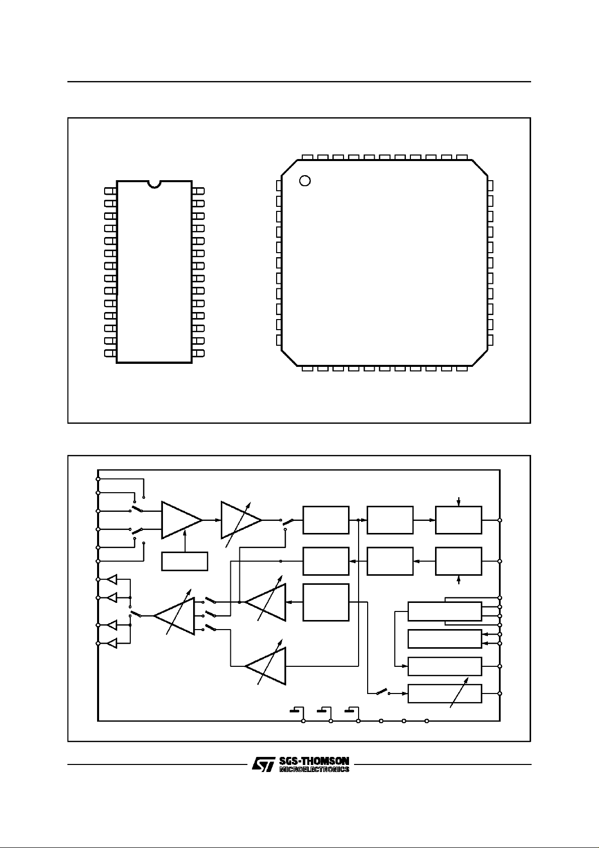
ST5092
PIN CONNECTIONS (Topview)
N.C.
N.C.
VCCP
VCCA
44 43 42 41 3940 38 37 36 35 34
N.C.
N.C.
MIC3+
MIC3-
GNDA
N.C.
MIC1+
N.C.
V
CCA
V
CCP
N.C.
V
Fr-
V
Fr+
V
Lr-
V
Lr+
GNDP MCLK
D
2
3
4
5
6
SO28
7
8
9
10
R
CCLK
CS-
CI CO
12
13
28
27
26
25
24
23
22
21
20
19
18
17
16
1514BZ V
D94TL094
BLOCK DIAGRAM
MIC3+1
MIC3GNDA
MIC1+
MIC1MIC2+
MIC2LO
FS
GND11
D
x
CC
N.C.
VFr-
VFr+
N.C.
VLr-
VLr+
N.C.
GNDP
N.C.
DR
N.C.
1
2
3
4
5
6
7
8
9
10
12 13 14 15 16
N.C.
N.C.
CCLK
TQFP44
171118 19 20 21 22
CI
CS-
BZ
VCC
CO
DX
GND
N.C.
33
32
31
30
29
28
27
26
25
24
23
MIC1-
N.C.
MIC2+
MIC2-
N.C.
N.C.
N.C.
LO
MCLK
FS
N.C.
D94TL095
2/29
MIC3-
MIC2-
MIC1-
MIC2+
MIC1+
MIC3+
VFr-
VFr+
VLr-
VLr+
EARA OUTPUT
-1
12dB
1
OE
-1
12dB
1
EXTA OUTPUT
MIC
PREAMP
20dB
+ MUTE
VS & TE
0 -> -30dB,
2dB STEP
RTE
SE
SI
D93 TL074
AMP
MIC
0 -> 22.5
1.5dB STEP
TONE
0 -> -27dB
3dB STEP
SIDETONE
-12.5 -> -27.5dB
1dB STEP
AMP
PREFILTER &
DE
(A)
(B)
AMP
BANDPASS
FILTER
BANDPASS
FILTER
TONE, RING
& DTMF
GENER.
& FILTER
GNDP GNDA GND VCCA VCC VCCP
PCM ADC
PCM DAC
BE
EN
TRANSMIT
REGISTER
RECEIVE
REGISTER
EN
CONTROL INTERFACE
µ-WIRE
CLOCK GENERATOR
& SYNCHRONIZER
INTERFACE LATCH
BUZZER
DRIVER
LEVEL
ADJUST
(PWM)
DX
DR
CO
CI
CSCCLK
MCLK
FS
LO
BZ

PIN FUNCTIONS(SO28)
Pin Name Description
1 N.C. Not Connected.
2V
3V
4 N.C. Not Connected.
5,6 V
7,8 V
Fr+,VFr–
Lr+,VLr–
9 GNDP Power ground. V
10 D
11 CCLK Control Clock input: Thisclock shifts serial control information into CI and out from CO when the
12 CS- Chip Select input: Whenthis pin is low, controlinformation is written into and outfrom the ST5092
13 CI Control data Input: SerialControl information is shifted into theST5092 on this pin when CS- is low
14 BZ Pulse widthmodulated buzzer driver output.
15 V
16 CO Controldata Output: Serial control/statusinformation isshifted out from the ST5092 on this pin
17 D
18 GND Ground: All digital signalsare referenced to this pin.
19 FS Frame Sync input: This signal is a 8kHz clock whichdefines thestart of the transmit andreceive
20 MCLK MasterClockInput:Thissignal isusedby theswitchedcapacitorfiltersandthe encoder/decoder
21 LO A logic 1 written intoDO (CR1) appears at LO pin as a logic 0
22 MIC2- Secondnegativehigh impedanceinput to transmit pre-amplifier for microphoneconnection.
23 MIC2+ SecondPositivehigh impedance inputto transmitpre-amplifier for microphone connection.
24 MIC1- Negativehigh impedanceinputto transmitpre-amplifier for microphoneconnection.
25 MIC1+ Positivehighimpedance input to transmitpre-amplifier for microphone connection.
26 GNDA Analog Ground: All analogsignals arereferenced tothis pin.GND and GNDA must be connected
27 MIC3- Thirdnegativehigh impedance outputtotransmitpreamplifier formicrophone connection.
28 MIC3+ Thirdpositive high impedance outputto transmit preamplifier for microphone connection.
Positive power supplyinput for the analog section.
CCA
V
and V
CC
Positive power supplyinput for the power section.V
CCP
must be direc t ly conn ec ted toget her.
CCA
and VCCmust be connected together.
CCP
Receive analog earpiece amplifier complementary outputs.Theseoutputscan drive directly earpiece
transductor. Thesignalat this output canbe the sum of:
- Receive Speech signal from D
,
R
- Internal Tone Generator,
- Sidetone signal.
Receive analogextra amplifier complementary outputs. The signalat these outputs can be the
sum of:
- Receive Speech signal from DR,
- Internal Tone generator,
- Sidetone signal.
and VLrdriver are referencedto thispin. GNDP and GND must be connected
Fr
together close tothe device.
Receive datainput:Data is shiftedin during the assigned Received timeslots In delayed andnon-
R
delayed normalframesynchr.modes voicedata byteis shiftedin at the MCLKfrequency on the
fallingedges ofMCLK, whilein non-delayed reverseframe synchr.mode voice data byteis shiftedin
at theMCLKfrequency onthe risingedges of MCLK.
CS- input is low, depending on the current instruction. CCLK may be asynchronous with the other
system clocks.
via CI andCO pins.
on the rising edgesof CCLK.
Positive power supplyinput for the digital section.
CC
when CS- islow on the falling edges of CCLK.
Transmit Data ouput:Data is shifted out onthis pin during the assigned transmittime slots.
X
Elsewhere D
synchr. modes, voicedata byte is shifted out from TRISTATE output D
output is in the high impedance state. In delayed andnon-delayed normal frame
X
at the MCLKon the rising
X
edge of MCLK,while in non-delayed reverse frame synchr mode voice databyte is shiftedout on
the falling edge of MCLK.
frames. Any ofthree formats may be used for this signal: non delayed normal mode, delayed
mode, and non delayed reverse mode.
sequencing logic.Values mustbe 512 kHz,1.536MHz,2.048MHz or2.56MHzselected bymeansof
ControlRegisterCRO. MCLKis usedalso toshift-inandout data.
A logic 0 written intoDO (CR1) appears at LO pin as a logic1.
together close tothe device.
ST5092
3/29

ST5092
PIN FUNCTIONS(TQFP44)
Pin Name Description
1 N.C. Not Connected.
2,3 V
Fr+,VFr–
4 N.C. Not Connected.
5,6 V
Lr+,VLr–
7 N.C. Not Connected.
8 GNDP Power ground. V
9 N.C. Not Connected.
10 D
11,12,13 N.C. Not Connected.
14 CCLK Control Clock input: Thisclock shifts serial control information into CI and out from CO when the
15 CS- Chip Select input: Whenthis pin is low, controlinformation is written into and outfrom the ST5092
16 CI Control data Input: SerialControl information is shifted into theST5092 on this pin when CS- is low
17 BZ Pulse widthmodulated buzzer driver output.
18 V
19 CO Controldata Output: Serial control/statusinformation isshifted out from the ST5092 on this pin
20 D
21 GND Ground: All digital signalsare referenced to this pin.
22,23 N.C. Not Connected.
24 FS Frame Sync input: This signal is a 8kHz clock whichdefines thestart of the transmit andreceive
25 MCLK MasterClockInput:Thissignal isusedby theswitchedcapacitorfiltersandthe encoder/decoder
26 LO A logic 1 written intoDO (CR1) appears at LO pin as a logic 0
27,28,29 N.C. Not Connected.
30 MIC2- Secondnegativehigh impedance input to transmit pre-amplifier for microphoneconnection.
31 MIC2+ SecondPositivehigh impedance inputto transmitpre-amplifier for microphone connection.
32 N.C. Not Connected.
33 MIC1- Negativehigh impedanceinputto transmitpre-amplifier formicrophone connection.
34 MIC1+ Positivehighimpedance input to transmitpre-amplifier formicrophone connection.
35 N.C. Not Connected.
36 GNDA Analog Ground: All analogsignals arereferenced tothis pin.GND and GNDA must be connected
37 MIC3- Thirdnegative high impedance outputto transmitpreamplifier formicrophone connection.
38 MIC3+ Thirdpositive high impedance outputto transmit preamplifier for microphone connection.
39,40 N.C. Not Connected.
41 V
42 V
43,44 N.C. Not Connected.
Receive analog earpiece amplifier complementary outputs.Theseoutputscan drive directly earpiece
transductor. Thesignalat this output canbe the summof:
- Receive Speech signal from D
,
R
- Internal Tone Generator,
- Sidetone signal.
Receive analog extraamplifiercomplementary outputs. Thesignalat these outputs can bethesumof:
- Receive Speech signal from DR,
- Internal Tone generator,
- Sidetone signal.
and VLrdriver are referencedto thispin. GNDP and GND must be connected
Fr
together close tothe device.
Receive datainput: Datais shifted in during the assignedReceived time slots In delayed and non-
R
delayed normal frame synchr. modes voice data byte is shiftedin at the MCLK frequency onthe
falling edges of MCLK, while in non-delayed reverse frame sinchr. mode voice data byte isshifted
in at the MCLK frequency on the risingedges of MCLK.
CS- input is low, depending on the current instruction. CCLK may be asynchronous with the other
system clocks.
via CI andCO pins.
on the rising edgesof CCLK.
Positive power supplyinput for the digital section.
CC
when CS- islow on the falling edges of CCLK.
Transmit Dataouput:Data isshiftedouton this pinduring theassignedtransmittimeslots.Elsewhere
X
D
outputis inthe high impendance state.Indelayed andnon-delayednormalframesynchr.modes,
X
voicedata byte isshiftedoutfromTRISTATEoutput D
attheMCLK onthe risingedgeof MCLK,while
X
innon-delayed reverse framesynchrmode voice databyteisshiftedouton thefallingedge ofMCLK.
frames. Either of threeformats may be used for this signal: non delayed normalmode, delayed
mode, and non delayed reverse mode.
sequencing logic.Values mustbe 512 kHz,1.536MHz,2.048MHz or2.56MHzselected bymeansof
ControlRegisterCRO. MCLKis usedalso toshift-inandoutdata.
A logic 0 written intoDO (CR1) appears at LO pin as a logic1.
together close tothe device.
Positive power supplyinput for the analog section.
CCA
V
and V
CC
Positive power supplyinput for the power section.V
CCP
must be direc t ly conn ec ted toget her.
CCA
and VCCmust be connected together.
CCP
4/29

ST5092
FUNCTIONAL DESCRIPTION
I DEVICEOPERATION
I.1 Poweron initialization:
When power is first applied, power on reset circuitry initializes ST5092 and puts it into the power
down state.Gain ControlRegistersforthe various
programmable gain amplifiers and programmable
switches are initialized as indicated in theControl
Register description section. All CODEC functions
are disabled.
The desired selection for all programmable functions may be intialized prior to a power up command using the MICROWIRE control channel.
I.2 Powerup/down control:
Following power-on initialization, power up and
power down controlmay be accomplishedby writing any of the control instructions listed in Table 1
into ST5092with ”P”bit set to 0 for power up or 1
for power down.
Normally, it is recommended that all programmable functions be initially programmed while the
device is powered down. Power state control can
then be included with the last programming instruction or in a separatesingle byte instruction.
Any of the programmable registers may also be
modified whileST5092 is powered up ordown by
setting ”P” bit as indicated. When power up or
down control is entered as a single byte instruction, bit 1 must be set to a 0.
When a power up command is given, all de-activated circuits are activated, but output D
will re-
X
main in the highimpedance state until the second
Fs pulse after power up.
I.3 Powerdown state:
Following a period of activity, power down state
may be reentered by writing a power down instruction.
Control Registers remain in their currentstate and
can be changed by MICROWIRE control interface.
In addition to the power down instruction, detection of loss MCLK (no transition detected) automatically entersthe device in ”reset” power down
state withD
I
.4 Transmit section:
Transmit analog interface is designed in two
stages to enable gains up to 42.5 dB to be realized. Stage 1 is a low noise differential amplifier
providing 20 dB gain. A microphone may be capacitevely connected to MIC1+, MIC1- inputs,
while the MIC2+ MIC2– and MIC3+ MIC3- inputs
may be usedto capacitivelyconnect a secondmicrophone or a thirdmicrophone respectivelyor an
auxiliary audio circuit. MIC1 or MIC2 or MC3 or
transmit mute is selected with bits 6 and 7 of register CR4.
outputin the high impedancestate.
X
In the mute case, the analog transmit signal is
grounded and the sidetone path is also disabled.
Following the first stage is a programmable gain
amplifier which provides from 0 to 22.5 dB of additional gain in 1.5dBstep.The total transmit gain
should be adjusted so that, at reference point A,
see Block Diagram description, the internal 0
dBm0 voltage is 0.49 Vrms (overload level is 0.7
Vrms). Second stage amplifier gain can be programmedwith bits 4 to 7 ofCR5.
An active RC prefilter then precedesthe8th order
band pass switched capacitor filter. A/D converter
can be either a 14-bitlinear(bit CM= 0 in register
CR0) or can have a compressing characteristics
(bit CM = 1 in registerCR0) according to CCITT A
or MU255 coding laws. A precision on chip voltage referenceensuresaccurate and highlystable
transmission levels.
Any offset voltage arisingin the gain-setamplifier,
the filtersor the comparator is cancelled by an internalautozerocircuit.
Each encode cycle begins immediatly at the beginning of the selected Transmit time slot. The total signal delay referenced to the start of the time
slot is approximatively195 µs (due to the transmit
filter) plus 125 µs (due to encoding delay), which
totals 320µs. Voicedata is shifted out on D
X
during the selected time slot on the transmit rising
edges of MCLK in delayedor non-delayednormal
mode or on the falling edges of MCLK in non-delayed reversemode.
I.5 Receive section:
Voice Data is shifted into the decoder’s Receive
voice data Register via the D
lected time slot on the falling edges of MCLK in
delayed or non-delayed normal mode or on the
rising edges of MCLK in non-delayed reverse
mode.
The decoder consists of either a 14-bit linear or
an expanding DAC with A or MU255 law decoding characteristic. Following the Decoder is a
3400 Hz 8th order band-pass switched capacitor
filter withintegral Sin X/X correction for the 8 kHz
sampleand hold.
0 dBmO voltage at this (B) reference point (see
Block Diagram description) is 0.49 Vrms. A transcient suppressing circuitry ensure interference
noise suppressionat power up.
The analog speech signal output can be routed
eitherto earpiece (V
tra analog output (V
FR+,VFR-
,V
Lr+
bits OE and SE(1 and 0 of CR4).
Total signal delay is approximatively 190µs (filter
plus decoding delay) plus 62.5 µs (1/2 frame)
whichgives approximatively252 µs.
Differential outputs V
FR+,VFR-
rectly drive an earpiece. Preceding the outputs is
a programmableattenuationamplifier, which must
pin during the se-
R
outputs)or to an ex-
outputs) by setting
Lr-
are intended to di-
5/29

ST5092
be set bywriting to bits 4 to 7 in register CR6. Attenuationsin the range 0 to -30 dB relativeto the
maximum level in 2 dB step can be programmed.
The input of this programmable amplifier is the
sum of several signals which can be selected by
writing to registerCR4.:
- Receive speech signal which has been decodedand filtered,
- Internally generated tone signal, (Tone amplitudeis programmedwith bits4 to7 of register
CR7),
- Sidetonesignal, the amplitude of which is programmedwithbits 0 to 3 ofregisterCR5
V
FR+
andV
outputsarecapableofdriving output
FR-
power level up to 66mW into differentially connectedload impedance of 30 Ω. Piezoceramicreceivers up to50nF can also be driven.
Differential outputs V
Lr+,VLr-
are intended to directly drive anextra output. Preceding the outputs
is a programmable attenuation amplifier, which
must be set by writing to bits 0 to 3 in register
CR6. Attenuationsin the range 0 to -30 dB relative to the maximum level in 2.0 dB step can be
programmed. The input ofthis programmable amplifier can be the sumof signalswhich canbe selected by writingto register CR4:
- Receive speech signal which has been decodedand filtered,
- Internally generated tone signal, (Tone amplitudeis programmedwith bits4 to7 of register
CR7),
- Sidetonesignal, the amplitude of which is programmedwithbits 0 to 3 ofregisterCR5.
and V
V
Lr+
outputsare capableof drivingoutput
Lr-
power level up to 66mW into differentially connected loadimpedanceof 30 Ω. Piezoceramicreceivers up to50nF can also be driven.
Non delayed data mode is similar to long frame
timing on ST5080A: first time slot begins nominally coincident with the rising edge of F
. Alter-
S
native is to use delayeddata mode, which is similar to short frame sync timing on ST5080A, in
which F
input must be high at least a half cycle
S
of MCLK earlier the frame beginning. In the case
of companded code only (bit CM = 1 in register
CRO) a time slot assignment circuit on chip may
be used with all timing modes, allowing connection to one of thetwo B1 and B2voice data channels.
Two data formats are available: in Format 1, time
slot B1 corresponds to the 8 MCLK cycles following immediately the rising edge of FS, while time
slot B2 corresponds to the 8 MCLK cycles following immediately time slot B1.
In Format 2, time slot B1 is identical to Format 1.
Time slot B2 appears two bit slots after time slot
B1. This two bits space is left available for insertion of the D channel data.
Data format is selected by bit FF (2) in register
CR0. Time slot B1 or B2 is selected by bit TS (1)
in Control Register CR1.
Bit EN (2) in control register CR1 enables or disables the voice data transfer on D
and DRas
X
appropriate. During the assigned time slot, D
output shifts data out from the voice data register
on the rising edges of MCLK in the case of delayed and non-delayed normal modes or on the
falling edges of MCLK in the case of non-delayed
reverse mode. Serial voice data is shifted into D
input during the same time slot on the falling
edges of MCLK in the case of delayed and nondelayed normal modes or on the rising edges of
MCLK in thecaseof non-delayedreversemode.
D
is in the high impedance Tristate condition
X
when in thenon selected time slots.
X
R
BUZZER OUTPUT:
Single ended output BZ is intended to drive a
buzzer, via an external BJT, with a squarewave
pulse width modulated (PWM) signal the frequency of whichis storedinto registerCR8.
For some applicationsit is also possible to amplitude modulate this PWM signal with a squarewave signal having a frequency stored in register
CR9.
Maximum load for BZis 5kΩand 50pF.
I.6 DigitalInterface (Fig.1)
F
FrameSync inputdetermines the beginningof
S
frame. It may have any durationfrom a singlecycle of MCLK to a squarewave.Three different relationships may be established between the
Frame Sync input and the first time slot of frame
by setting bits DM1 and DM0 in register CR1.
6/29
I.7 Control Interface:
Control information or data is written into or readback from ST5092via the serial control port consisting of control clock CCLK, serial data input CI
and output CO, and Chip Select input, CS-. All
controlinstructions require 2 bytes as listedin Table 1, with the exception of a single byte powerup/down command.
To shift control data into ST5092, CCLK must be
pulsed high 8 times while CS- is low. Data on CI
input is shifted into the serial input register on the
rising edge of each CCLK pulse. After all data is
shifted in, the contentof the input shift register is
decoded, and may indicate that a 2nd byte of
control data will follow. This second byte may
either be defined by a second byte-wide CSpulse or may follow the first contiguously, i.e. it is
not mandatory for CS- to return high in between
the first and second control bytes. At the end of
the 2nd control byte, data is loaded into the ap-
Figure 1: DigitalInterface Format (*)
FORMAT 1
(delayed timing)F5
ST5092
F6
MCLK
DR
DX
F9
MCLK
DR
DX
FORMAT 2
(non delayed timing)
XB2B1 XX
B2B1
(delayed timing)F8
(non delayed timing)
XB2B1 XX
B2B1
D93TL075
(*) Significant Only For CompandedCode.
propriate programmable register. CS- mustreturn
high atthe end of the 2nd byte.
To read-backstatus informationfrom ST5092,the
first byte of the appropriate instruction is strobed
in during the first CS- pulse, as defined in Table
1. CS- must be set low for a further 8 CCLK cycles, during which data is shifted out of the CO
pin onthe falling edges of CCLK.
When CS- is high, CO pin is in the high impedance Tri-state, enabling CO pins of several devices to be multiplexedtogether.
Thus, to summarise,2 byte READ and WRITEinstructions may use either two 8-bit wide CSpulses or a single 16 bit wide CS- pulse.
I
.8 Control channel access to PCMinterface:
It is possible to access the B channel previously
selected in Register CR1 in the case of compandedcode only.
A byte written into Control Register CR3 will be
automatically transmitted from D
output in the
X
followingframein placeof the transmitPCM data.
A byte written into Control Register CR2 will be
automatically sent through the receive path to the
Receiveamplifiers.
In order to implement a continuousdata flow from
the Control MICROWIRE interface to a B channel, it is necessary to send the control byte on
each PCM frame.
A current byte received on D
input can be read
R
in the register CR2. In order to implement a continuous data flow from a B channel to MICROWIREinterface,it is necessary to read register CR2 at eachPCM frame.
7/29

ST5092
II
PROGRAMMABLE FUNCTIONS
For both formats of Digital Interface, programmable functions are configured by writing to a number ofregistersusing a 2-byte write cycle.
verification. Byte one is always register address,
while byte two is Data.
Table 1 lists the register set and their respective
adresses.
Most of these registers can also be read-back for
Table 1: ProgrammableRegisterIntructions
Function Address byte
76543210
Single byte Power up/down P X X X X X 0 X none
Write CR0 P 0 00001XseeCR0TABLE 2
Read-back CR0 P 0 00011XseeCR0
Write CR1 P 0 00101XseeCR1TABLE 3
Read-back CR1 P 0 00111XseeCR1
Write Data toreceive path P 0 01001XseeCR2TABLE 4
Read datafromD
Write Data toD
Write CR4 P 0 10001XseeCR4TABLE 6
Read-back CR4 P 0 10011XseeCR4
Write CR5 P 0 10101XseeCR5TABLE 7
Read-back CR5 P 0 10111XseeCR5
Write CR6 P 0 11001XseeCR6TABLE 8
Read-back CR6 P 0 11011XseeCR6
Write CR7 P 0 11101XseeCR7TABLE 9
Read-back CR7 P 0 11111XseeCR7
Write CR8 P 1 00001XseeCR8TABLE 10
Read-back CR8 P 1 00011XseeCR8
Write CR9 P 1 00101XseeCR9TABLE 11
Read-back CR9 P 1 00111XseeCR9
Write CR10 P 1 01001XseeCR10 TABLE12
Read-back CR10 P 1 01011XseeCR10
Write CR11 P 1 01101XseeCR11 TABLE13
Read-back CR11 P 1 01111XseeCR11
Write Test RegisterCR14 P 1 11001Xreserved
R
X
P001011XseeCR2
P001101XseeCR3TABLE 5
Data byte
NOTE 1: bit 7 of the address byte and data byte is alwaysthe firstbit clocked intoor out from:CI andCO pins when MICROWIREserial
NOTE 2: ”P” bit is Power up/down Control bit.P = 1 Means Power Down.
NOTE 3: Bit 2 is write/read select bit.
NOTE 4: Registers CR12, CR13, and CR15 are not accessible.
8/29
port is enabled.
X = reserved: write 0
Bit 1 indicates,if set, the presence ofa secondbyte.
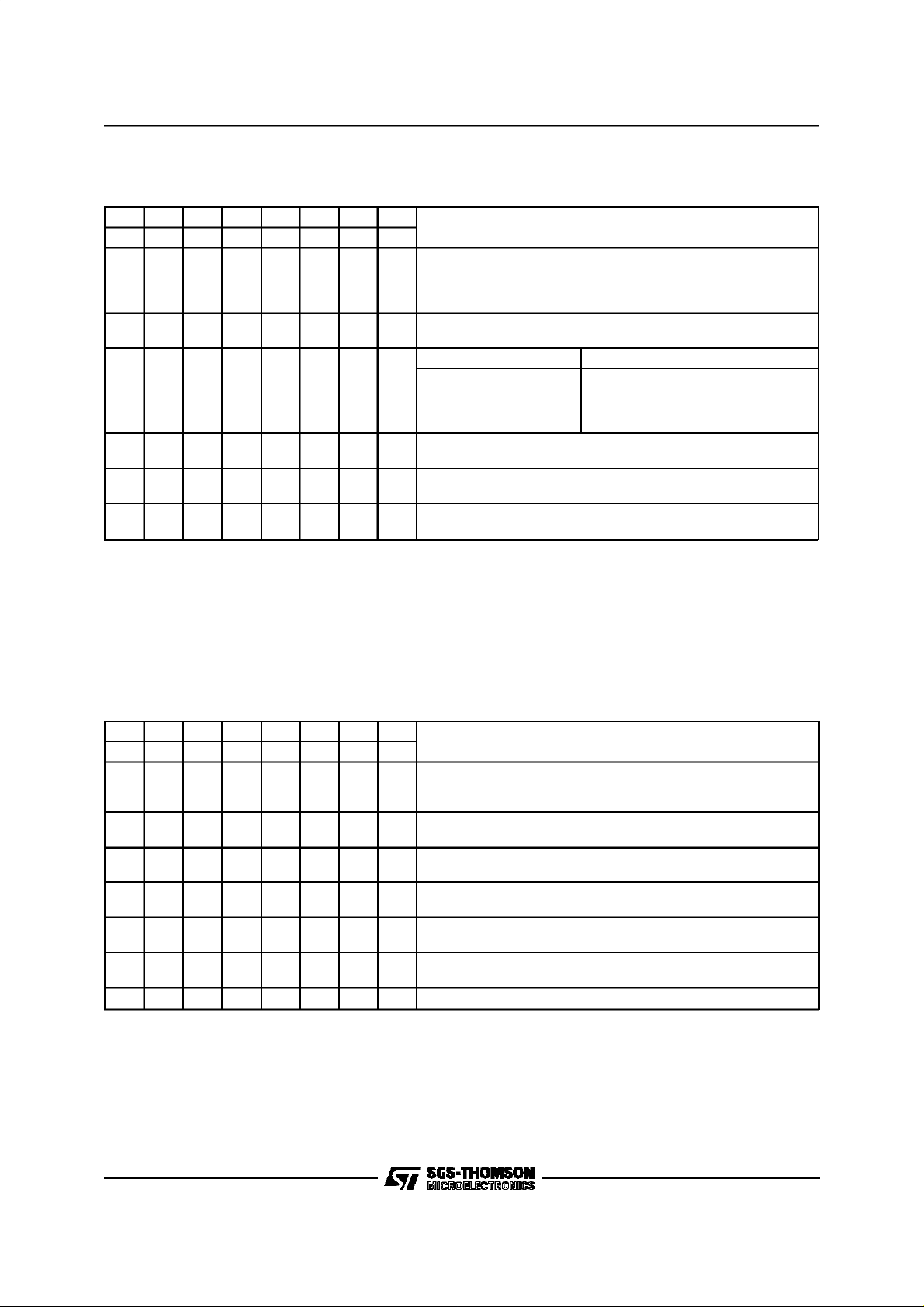
Table 2: ControlRegisterCR0Functions
ST5092
76543210
F1 F0 CM MA IA FF B7 DL
0
0
1
0
0
1
1
1
0
1
0
0
1
0
0
1
1
1
0
1
0
1
*: state at power on initialization
(1): significant in compandedmode only
MCLK = 512 kHz
MCLK = 1.536 MHz
MCLK = 2.048 MHz
MCLK = 2.560 MHz
Linear code
Companded code
Linear Code Companded Code
2-complement *
sign and magnitude
2-complement
1-complement
B1 and B2 consecutive
B1 and B2 separated
8 bits time-slot
7 bits time-slot
01Normal operation
Digital Loop-back
Function
*
*
MU-law: CCITT D3-D4 *
MU-law: Bare Coding
A-law including even bit inversion
A-law:Bare Coding
* (1)
(1)
* (1)
(1)
*
Table 3: Control Register CR1 Functions
76543210
DM1 DM0 DO MR MX EN TS
0
X
1
0
1
1
0
1
0
1
0
1
0
1
0
1
*: state at power on initialization
(1):
X:
significant in companded mode only
reserved: write 0
delayed data timing
non-delayed normal datatiming
non-delayed reverse datatiming
L0 latch set to 1
L0 latch set to 0
D
connected to rec.path
R
CR2 connected torec. path
Trans path connected to D
CR3 connected toD
X
voice data transferdisable
voice data transferenable
B1 channel selected
B2 channel selected
X
Function
X
*
*
*
(1)
*
(1)
*
* (1)
(1)
9/29
 Loading...