

SGS Thomson Microelectronics ST5090ADTR, ST5090AD, ST5090TQFPTR, ST5090TQFP Datasheet

LOW VOLTAGE 14-BIT LINEAR CODEC
WITH HIGH-PERFORMANCEAUDIO FRONT-END
FEATURES:
Complete CODEC and FILTER systemincluding:
14 BIT LINEAR ANALOG TO DIGITAL AND
DIGITALTO ANALOGCONVERTERS.
8 BIT COMPANDED ANALOG TO DIGITAL
AND DIGITAL TO ANALOG CONVERTERS
A-LAW OR µ-LAW.
TRANSMIT AND RECEIVE BAND-PASSFILTERS
ACTIVEANTIALIAS NOISEFILTER.
PhoneFeatures:
THREE SWITCHABLE MICROPHONE AMPLIFIER INPUTS. GAIN PROGRAMMABLE:
20 dB PREAMP. (+MUTE), 0 . . 22.5 dB AMPLIFIER,1.5 dB STEPS.
EARPIECE AUDIO OUTPUT. ATTENUATION
PROGRAMMABLE:0 .. 30 dB, 2 dB STEPS.
EXTERNAL AUDIO OUTPUT. ATTENUATION
PROGRAMMABLE:0 .. 30 dB, 2 dB STEPS.
TRANSIENT SUPRESSION SIGNAL DURING
POWER ON AND DURING AMPLIFIER
SWITCHING.
INTERNAL PROGRAMMABLE SIDETONE
CIRCUIT. ATTENUATION PROGRAMMABLE:
16 dB RANGE, 1 dB STEP. ROUTINGPOSSIBLE TO BOTHOUTPUTS.
INTERNALRING ORTONE GENERATOR INCLUDING DTMF TONES, SINEWAVE OR
SQUAREWAVE WAVEFORMS. ATTENUATION PROGRAMMABLE: 27dB RANGE,
3dB STEP. THREE FREQUENCY RANGES:
a) 3.9Hz . . . . 996Hz, 3.9Hz STEP
b) 7.8Hz . . . . 1992Hz, 7.8Hz STEP
c) 15.6Hz. . .. 3984Hz, 15.6Hz STEP
PROGRAMMABLE PULSE WIDTH MODULATEDBUZZER DRIVEROUTPUT.
GeneralFeatures:
SINGLE 3.3V ±10% OR 5V ±10% SUPPLY
SELECTABLE.
EXTENDED TEM PER A T U RE RANGE OPERATION(*)-40°Cto85°C.
1.5 µW STANDBYPOWER(TYP. AT 3V).
21 mW OPERATINGPOWER (TYP. AT3V).
CMOSCOMPATIBLEDIGITAL INTERFACES.
PROGRAMMABLE PCM AND CONTROL IN-
TERFACEMICROWIRE COMPATIBLE.
ST5090
TQFP44(10x10x1.4)
ORDERING NUMBERS:
Package Dim. Cond.
ST5090AD
ST5090ADTR
ST5090TQFP
ST5090TQFPTR
SO28
SO28
TQFP44
TQFP44
APPLICATIONS:
GSM DIGITAL CELLULAR TELEPHONES.
CT2 DIGITALCORDLESSTELEPHONES.
DECTDIGITAL CORDLESSTELEPHONES.
BATTERY OPERATED AUDIO FRONT-ENDS
FORDSPs.
(*) Functionality guaranteed in the range – 40°C to +85°C;
Timing and Electrical Specifications are guaranteed in the range
–30°C to +85°C.
GENERALDESCRIPTION
ST5090is a highperformancelow power combined
PCM CODEC/FILTERdevicetailored to implement
the audio front-end functions required by the next
generation low voltage/low power consumption
digitalterminals.
ST5090 offers a number of programmable functionsaccessedthrougha serial controlchannelthat
easilyinterfacesto any classical microcontroller.
ThePCM interfacesupportsboth non-delayed(normal and reverse) and delayed frame synchronizationmodes.
ST5090can be configurated either as a 14-bit linearor as an 8-bitcompandedPCMcoder.
Additionally to the CODEC/FILTER function,
ST5090 includes a Tone/Ring/DTMF generator, a
sidetonegeneration,and abuzzerdriveroutput.
ST5090fulfills and exceedsD3/D4and CCITTrecommendations and ETSI requirements for digital
handsetterminals.
Main applicationsinclude digital mobile phones,as
cellular and cordless phones, or any batterypoweredequipmentthat requires audio codecsoperatingatlow singlesupplyvoltages
SO28
10x10x1.4
10x10x1.4
Tube
Tape&Reel
Tray 8x20
Tape&Reel
February 1996
This is advanced informationon a new product now in development or undergoing evaluation. Details are subject to change without notice.
1/29
ST5090
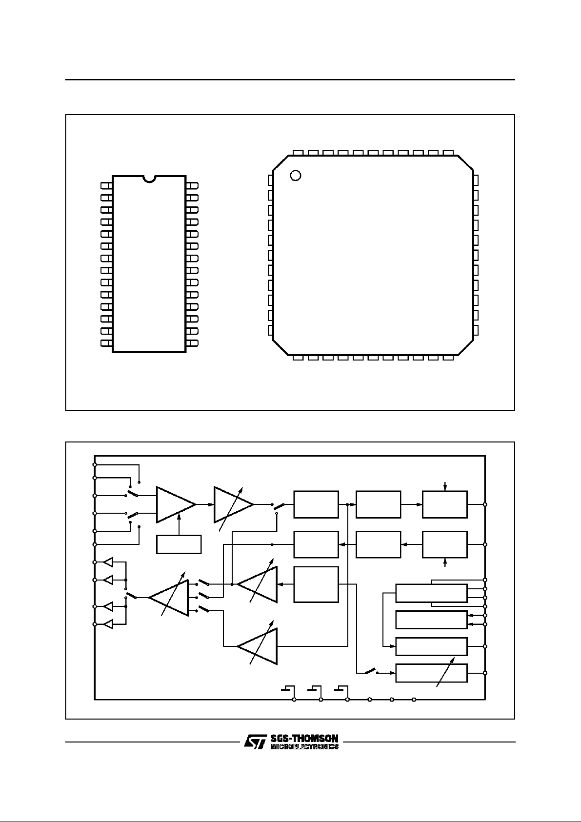
PIN CONNECTIONS(Top view)
N.C.
N.C.
VCCP
VCCA
44 43 42 41 3940 38 37 36 35 34
N.C.
N.C.
MIC3+
MIC3-
GNDA
N.C.
MIC1+
N.C.
V
CCA
V
CCP
N.C.
V
Fr-
V
Fr+
V
Lr-
V
Lr+
GNDP MCLK
D
2
3
4
5
6
SO28
7
8
9
10
R
CCLK
CS-
CI CO
12
13
28
27
26
25
24
23
22
21
20
19
18
17
16
1514BZ V
D94TL094
BLOCKDIAGRAM
MIC3+1
MIC3GNDA
MIC1+
MIC1MIC2+
MIC2LO
FS
GND11
D
x
CC
N.C.
VFr-
VFr+
N.C.
VLr-
VLr+
N.C.
GNDP
N.C.
DR
N.C.
1
2
3
4
5
6
7
8
9
10
12 13 14 15 16
N.C.
N.C.
CCLK
TQFP44
171118 19 20 21 22
CI
CS-
BZ
VCC
CO
DX
GND
N.C.
33
32
31
30
29
28
27
26
25
24
23
MIC1-
N.C.
MIC2+
MIC2-
N.C.
N.C.
N.C.
LO
MCLK
FS
N.C.
D94TL095
2/29
MIC3-
MIC2-
MIC1-
MIC2+
MIC1+
MIC3+
VFr-
VFr+
VLr-
VLr+
EARA OUTPUT
-1
12dB
1
OE
-1
12dB
1
EXTA OUTPUT
MIC
PREAMP
20dB
+ MUTE
VS & TE
0 -> -30dB,
2dB STEP
RTE
SE
SI
D93 TL074
MIC
AMP
0 -> 22.5
1.5dB STEP
TONE
0 -> -27dB
3dB STEP
SIDETONE
-12.5 -> -27.5dB
1dB STEP
AMP
PREFILTER &
DE
(A)
(B)
AMP
BANDPASS
FILTER
BANDPASS
FILTER
TONE, RING
& DTMF
GENER.
& FILTER
GNDP GNDA GND VCCA VCC VCCP
PCM ADC
PCM DAC
CONTROL INTERFACE
CLOCK GENERATOR
BE
EN
TRANSMIT
REGISTER
RECEIVE
REGISTER
EN
µ-WIRE
& SYNCHRONIZER
INTERFACE LATCH
BUZZER
DRIVER
LEVEL
(PWM)
DX
DR
CO
CI
CSCCLK
MCLK
FS
LO
BZ
ADJUST

PIN FUNCTIONS (SO28)
Pin Name Description
1 N.C. Not Connected.
2V
3V
4 N.C. Not Connected.
5,6 V
7,8 V
Fr+,VFr–
Lr+,VLr–
9 GNDP Power ground. V
10 D
11 CCLK Control Clock input: This clock shifts serial control information into CI and out from CO when the
12 CS- Chip Select input: When thispin is low, control information is writteninto and out from theST5090
13 CI Control data Input: Serial Control information isshifted into the ST5090 on this pin when CS- is low
14 BZ Pulse width modulated buzzer driver output.
15 V
16 CO Control data Output: Serialcontrol/status information is shifted out from the ST5090 on thispin
17 D
18 GND Ground: All digitalsignals are referenced to this pin.
19 FS Frame Sync input: This signal is a 8kHz clock which defines the start of the transmit and receive
20 MCLK Master ClockInput:Thissignalisusedbythe switchedcapacitor filtersandthe encoder/decoder
21 LO A logic1 written into DO (CR1) appears atLO pin as a logic 0
22 MIC2- Second negative high impedance input to transmit pre-amplifier formicrophoneconnection.
23 MIC2+ SecondPositive high impedance input to transmitpre-amplifier for microphone connection.
24 MIC1- Negative highimpedance inputtotransmitpre-amplifier formicrophone connection.
25 MIC1+ Positivehighimpedance input to transmit pre-amplifier for microphone connection.
26 GNDA Analog Ground: All analog signals are referenced to this pin. GND and GNDA must be connected
27 MIC3- Thirdnegative high impedance output to transmitpreamplifier formicrophone connection.
28 MIC3+ Third positive high impedance output to transmit preamplifier for microphone connection.
Positive power supply inputfor the analogsection.
CCA
+5V ±10% or 3.3V ±10% selec table. V
Positive power supply inputfor the powersection. 5V ±10% or 3.3V ±10% selectable V
CCP
V
must be connected together.
CC
CC
and V
must be direct ly c on nect ed toget h er .
CCA
Receiveanalog earpiece amplifier complementary outputs.These outputscandrive directlyearpiece
transductor. The signalat thisoutputcan bethesum of:
- Receive Speech signal from D
,
R
- Internal Tone Generator,
- Sidetone signal.
Receive analog extra amplifier complementary outputs. The signal at these outputs can bethe
sum of:
- Receive Speech signal from D
,
R
- Internal Tone generator,
- Sidetone signal.
and VLrdriver are referenced to this pin. GNDP and GND must be connected
Fr
together close to the device.
Receivedata input: Data isshifted in during the assigned Received timeslots Indelayedand non-
R
delayed normal frame synchr.modes voice databyte is shiftedin at the MCLK frequencyon the
fallingedges of MCLK, whilein non-delayed reverseframesynchr.mode voicedata byte isshiftedin
at the MCLK frequency onthe rising edges ofMCLK.
CS- input is low, depending on the currentinstruction. CCLK may beasynchronous with the other
system clocks.
via CI andCO pins.
on the rising edges of CCLK.
Positive power supply inputfor the digitalsection. +5V ±10% or 3.3V ±10% selectable.
CC
when CS- islow on the fallingedges of CCLK.
Transmit Data ouput: Data is shifted out onthis pinduring the assigned transmit timeslots.
X
Elsewhere D
synchr. modes, voicedata byte is shiftedout from TRISTATE output D
output is in the high impedance state.In delayed and non-delayed normal frame
X
at the MCLK on the rising
X
edge of MCLK, while in non-delayed reverse frame synchr mode voice data byte isshifted outon
the falling edge of MCLK.
frames. Any ofthree formats may be used forthis signal: non delayed normal mode, delayed
mode, and nondelayed reverse mode.
sequencinglogic.Valuesmustbe512 kHz, 1.536MHz, 2.048MHz or2.56MHz selectedbymeans of
ControlRegister CRO. MCLKisusedalsoto shift-inandout data.
A logic 0 written into DO (CR1) appears at LO pinas a logic 1.
together close to the device.
CCP
ST5090
and
3/29

ST5090
PIN FUNCTIONS (TQFP44)
Pin Name Description
1 N.C. Not Connected.
2,3 V
Fr+,VFr–
4 N.C. Not Connected.
5,6 V
Lr+,VLr–
7 N.C. Not Connected.
8 GNDP Power ground. V
9 N.C. Not Connected.
10 D
11,12,13 N.C. Not Connected.
14 CCLK Control Clock input: This clock shifts serial control information into CI and out from CO when the
15 CS- Chip Select input: When thispin is low, control information is writteninto and out from theST5090
16 CI Control data Input: Serial Control information isshifted into the ST5090 on this pin when CS- is low
17 BZ Pulse width modulated buzzer driver output.
18 V
19 CO Control data Output: Serialcontrol/status information is shifted out from the ST5090 on thispin
20 D
21 GND Ground: All digitalsignals are referenced to this pin.
22,23 N.C. Not Connected.
24 FS Frame Sync input: This signal is a 8kHz clock which defines the start ofthe transmitand receive
25 MCLK Master ClockInput:Thissignalisusedbythe switchedcapacitor filtersand the encoder/decoder
26 LO A logic1 written into DO (CR1) appears at LO pin as a logic 0
27,28,29 N.C. Not Connected.
30 MIC2- Second negative high impedance input to transmit pre-amplifierfor microphone connection.
31 MIC2+ SecondPositive high impedance input to transmitpre-amplifier for microphone connection.
32 N.C. Not Connected.
33 MIC1- Negative highimpedance inputtotransmitpre-amplifier formicrophone connection.
34 MIC1+ Positivehighimpedance input to transmit pre-amplifier formicrophone connection.
35 N.C. Not Connected.
36 GNDA Analog Ground: Allanalog signals are referenced to this pin. GND and GNDA must be connected
37 MIC3- Thirdnegative high impedance output to transmitpreamplifier for microphone connection.
38 MIC3+ Third positive high impedance output to transmit preamplifier for microphone connection.
39,40 N.C. Not Connected.
41 V
42 V
43,44 N.C. Not Connected.
Receiveanalog earpiece amplifier complementary outputs.These outputscandrive directlyearpiece
transductor. The signalat thisoutputcan bethesumm of:
- Receive Speech signal from D
,
R
- Internal Tone Generator,
- Sidetone signal.
Receiveanalog extra amplifiercomplementary outputs. The signal at theseoutputs can bethe sumof:
- Receive Speech signal from DR,
- Internal Tone generator,
- Sidetone signal.
and VLrdriver are referenced to this pin. GNDP and GND must be connected
Fr
together close to the device.
Receive data input: Datais shifted in during the assigned Received time slots In delayed and non-
R
delayed normal frame synchr.modes voice data byte is shifted in at the MCLK frequency on the
falling edges of MCLK, while in non-delayed reverse framesinchr. mode voice data byte is shifted
in at the MCLK frequency on the risingedges ofMCLK.
CS- input is low, depending on the currentinstruction. CCLK may beasynchronous with the other
system clocks.
via CI andCO pins.
on the rising edges of CCLK.
Positive power supply inputfor the digitalsection. +5V ±10% or 3.3V ±10% selectable.
CC
when CS- islow on the fallingedges of CCLK.
TransmitDataouput: Data is shiftedoutonthispinduring theassignedtransmittime slots.Elsewhere
X
D
outputis inthe highimpendance state.In delayed and non-delayed normalframesynchr. modes,
X
voicedatabyteisshiftedout from TRISTATEoutputD
atthe MCLK on the rising edgeof MCLK,while
X
innon-delayed reverseframesynchr mode voicedatabyte is shiftedout on the falling edgeof MCLK.
frames. Either of three formats may be used for this signal: non delayed normal mode, delayed
mode, and nondelayed reverse mode.
sequencinglogic.Valuesmustbe512 kHz, 1.536MHz, 2.048MHzor2.56MHzselectedbymeans of
ControlRegister CRO. MCLKisusedalsoto shift-inand out data.
A logic 0 written into DO (CR1) appears at LO pinas a logic 1.
together close to the device.
Positive power supply inputfor the analogsection.
CCA
+5V ±10% or 3.3V ±10% selec table. V
Positive power supply inputfor the powersection. 5V ±10% or 3.3V ±10% selectable V
CCP
V
must be connected together.
CC
CC
and V
must be direct ly c on nect ed toget h er .
CCA
CCP
and
4/29

ST5090
FUNCTIONAL DESCRIPTION
IDEVICE OPERATION
I.1 Poweron initialization:
When power is first applied, power on reset circuitry initializes ST5090 and puts it into the power
down state. GainControl Registersfor the various
programmable gain amplifiers and programmable
switches are initialized as indicated in the Control
Registerdescription section. AllCODEC functions
are disabled.
The desired selection for all programmable functions may be intialized prior to a power up commandusing theMICROWIREcontrol channel.
I.2 Powerup/down control:
Following power-on initialization, power up and
power down controlmay be accomplishedby writing any of thecontrol instructions listed in Table 1
into ST5090 with ”P” bit set to0 for power up or1
for power down.
Normally, it is recommendedthat all programmable functions be initially programmed while the
device is powered down. Power state control can
then be included with the last programming instructionor in a separatesingle byte instruction.
Any of the programmable registers may also be
modified while ST5090 is powered up or down by
setting ”P” bit as indicated. When power up or
down control is entered as a single byte instruction, bit 1 must be set toa 0.
When a power up command is given, all de-activated circuits are activated, but output D
will re-
X
main in the highimpedance state until the second
Fs pulse afterpower up.
I.3 Powerdown state:
Following a period of activity, power down state
may be reentered by writing a power down instruction.
Control Registersremain in their current stateand
can be changed by MICROWIRE control interface.
In addition to the power down instruction, detection of loss MCLK (no transition detected) automatically enters the device in ”reset” power down
statewith D
outputin the high impedance state.
X
I.4 Transmit section:
Transmit analog interface is designed in two
stages to enable gains up to 42.5 dB to be realized. Stage 1 is a low noise differential amplifier
providing 20 dB gain. A microphone may be capacitevely connected to MIC1+, MIC1- inputs,
while the MIC2+ MIC2– and MIC3+ MIC3- inputs
may be used to capacitivelyconnect a second microphone or a third microphone respectively or an
auxiliary audio circuit. MIC1 or MIC2 or MC3 or
transmit mute is selected with bits 6 and 7 of registerCR4.
In the mute case, the analog transmit signal is
grounded and the sidetone path is also disabled.
Following the first stage is a programmable gain
amplifier which provides from 0 to 22.5 dB of additional gain in 1.5dB step. The total transmit gain
should be adjusted so that, at reference point A,
see Block Diagram description, the internal 0
dBm0 voltage is 0.49 Vrms (overload level is 0.7
Vrms). Second stage amplifier gain can be programmed with bits 4 to 7 ofCR5.
An activeRC prefilterthen precedesthe 8th order
band pass switchedcapacitor filter. A/D converter
can be either a 14-bitlinear (bit CM = 0 in register
CR0) or can have a compressing characteristics
(bit CM = 1 in register CR0) accordingto CCITTA
or MU255 coding laws. A precision on chip voltage reference ensures accurate and highly stable
transmissionlevels.
Any offset voltagearising in the gain-setamplifier,
the filtersor the comparatoris cancelledby an internal autozero circuit.
Each encode cycle begins immediatly at the beginning of theselected Transmit time slot. The total signal delay referencedto the start of the time
slot isapproximatively 195 µs (due tothe transmit
filter) plus 125 µs (due to encoding delay), which
totals 320 µs. Voice data is shifted out on D
X
during the selected time slot on the transmit rising
edges of MCLK in delayed or non-delayed normal
mode or on the falling edges of MCLK in non-delayed reverse mode.
I.5Receive section:
Voice Data is shifted into the decoder’s Receive
voice data Register via the D
lected time slot on the falling edges of MCLK in
delayed or non-delayed normal mode or on the
rising edges of MCLK in non-delayed reverse
mode.
The decoder consists of either a 14-bit linear or
an expanding DAC with A or MU255 law decoding characteristic. Following the Decoder is a
3400 Hz 8th order band-pass switched capacitor
filter with integral Sin X/X correction for the8 kHz
sampleand hold.
0 dBmO voltage at this (B) reference point (see
Block Diagram description) is 0.49 Vrms. A transcient suppressing circuitry ensure interference
noise suppression at power up.
The analog speech signal output can be routed
eitherto earpiece(V
tra analog output (V
FR+,VFR-
Lr+,VLr-
bits OE and SE (1 and 0 of CR4).
Total signal delay is approximatively 190µs (filter
plus decoding delay) plus 62.5 µs (1/2 frame)
which gives approximatively252µs.
Differential outputs V
FR+,VFR-
rectly drive an earpiece. Preceding the outputs is
a programmableattenuationamplifier,which must
pin during the se-
R
outputs)or to an ex-
outputs) by setting
are intended to di-
5/29

ST5090
be set by writing to bits 4 to 7 in register CR6. Attenuations in the range 0 to -30 dB relative to the
maximum level in 2 dB step can be programmed.
The input of this programmable amplifier is the
sum of several signals which can be selected by
writing to register CR4.:
- Receive speech signal which has been decoded and filtered,
- Internally generated tone signal, (Tone amplitude isprogrammedwith bits 4 to 7 of register
CR7),
- Sidetone signal, the amplitude of which is programmed with bits 0 to3 ofregister CR5
V
FR+
and V
outputsare capableof driving output
FR-
power level up to 66mW into differentially connectedload impedanceof 30Ω. Piezoceramic receivers up to50nF can also be driven.
Differential outputs V
Lr+,VLr-
are intended to directlydrive an extraoutput. Precedingthe outputs
is a programmable attenuation amplifier, which
must be set by writing to bits 0 to 3 in register
CR6. Attenuations in the range 0 to -30 dB relative to the maximum level in 2.0 dB step can be
programmed. The input of this programmable amplifier can be the sumof signals which can be selected by writing to register CR4:
- Receive speech signal which has been decoded and filtered,
- Internally generated tone signal, (Tone amplitude isprogrammedwith bits 4 to 7 of register
CR7),
- Sidetone signal, the amplitude of which is programmed with bits 0 to3 ofregister CR5.
and V
V
Lr+
outputs are capable of driving output
Lr-
power level up to 66mW into differentially connectedload impedance of 30 Ω. Piezoceramic re-
ceivers up to50nF can also be driven.
Non delayed data mode is similar to long frame
timing on ST5080A: first time slot begins nominally coincident with the rising edge of F
. Alter-
S
native is touse delayed data mode, which is similar to short frame sync timing on ST5080A, in
which F
input must be high at least a half cycle
S
of MCLK earlier the frame beginning. In the case
of companded code only (bit CM = 1 in register
CRO) a time slot assignment circuit on chip may
be used with all timing modes, allowing connection to one of the two B1 and B2 voice data channels.
Two data formats are available:in Format 1, time
slot B1 corresponds to the 8 MCLK cycles following immediately the rising edge of FS, while time
slot B2 corresponds to the 8 MCLK cycles following immediatelytime slot B1.
In Format 2, time slot B1 is identical to Format 1.
Time slot B2 appears two bit slots after time slot
B1. This two bits space is left available for insertion of the D channel data.
Data format is selected by bit FF (2) in register
CR0. Time slot B1 or B2 is selected by bit TS (1)
in Control RegisterCR1.
Bit EN (2) in control register CR1 enables or disables the voice data transfer on D
and DRas
X
appropriate. During the assigned time slot, D
output shifts data out from the voicedata register
on the rising edges of MCLK in the case of delayed and non-delayed normal modes or on the
falling edges of MCLK in the case of non-delayed
reverse mode. Serial voice data is shifted into D
input during the same time slot on the falling
edges of MCLK in the case of delayed and nondelayed normal modes or on the rising edges of
MCLK in the caseof non-delayedreverse mode.
D
is in the high impedance Tristate condition
X
when in the non selected time slots.
X
R
BUZZEROUTPUT:
Single ended output BZ is intended to drive a
buzzer, via an external BJT, with a squarewave
pulse width modulated (PWM) signal the frequency ofwhich is stored into registerCR8.
For some applications it is also possible to amplitude modulate this PWM signal with a squarewave signal having a frequency stored in register
CR9.
Maximumload for BZ is 5kΩand 50pF.
I.6 DigitalInterface (Fig. 1)
F
Frame Sync input determines the beginning of
S
frame. It may have any durationfrom a single cycle of MCLK to a squarewave. Three different relationships may be established between the
Frame Sync input and the first time slot of frame
by setting bits DM1 and DM0 in register CR1.
6/29
I.7Control Interface:
Control information or data is written into or readback from ST5090 via the serial control port consisting of control clock CCLK, serial data input CI
and output CO, and Chip Select input, CS-. All
controlinstructions require 2 bytesas listed in Table 1, with the exception of a single byte powerup/down command.
To shiftcontrol data into ST5090, CCLK must be
pulsed high 8 times while CS- is low. Data on CI
input is shifted into the serial input register on the
rising edge of each CCLK pulse. After all data is
shifted in, the content of the input shift register is
decoded, and may indicate that a 2nd byte of
control data will follow. This second byte may
either be defined by a second byte-wide CSpulse or may follow the first contiguously, i.e. it is
not mandatory for CS- to return high in between
the first and second control bytes. At the end of
the 2nd control byte, data is loaded into the ap-
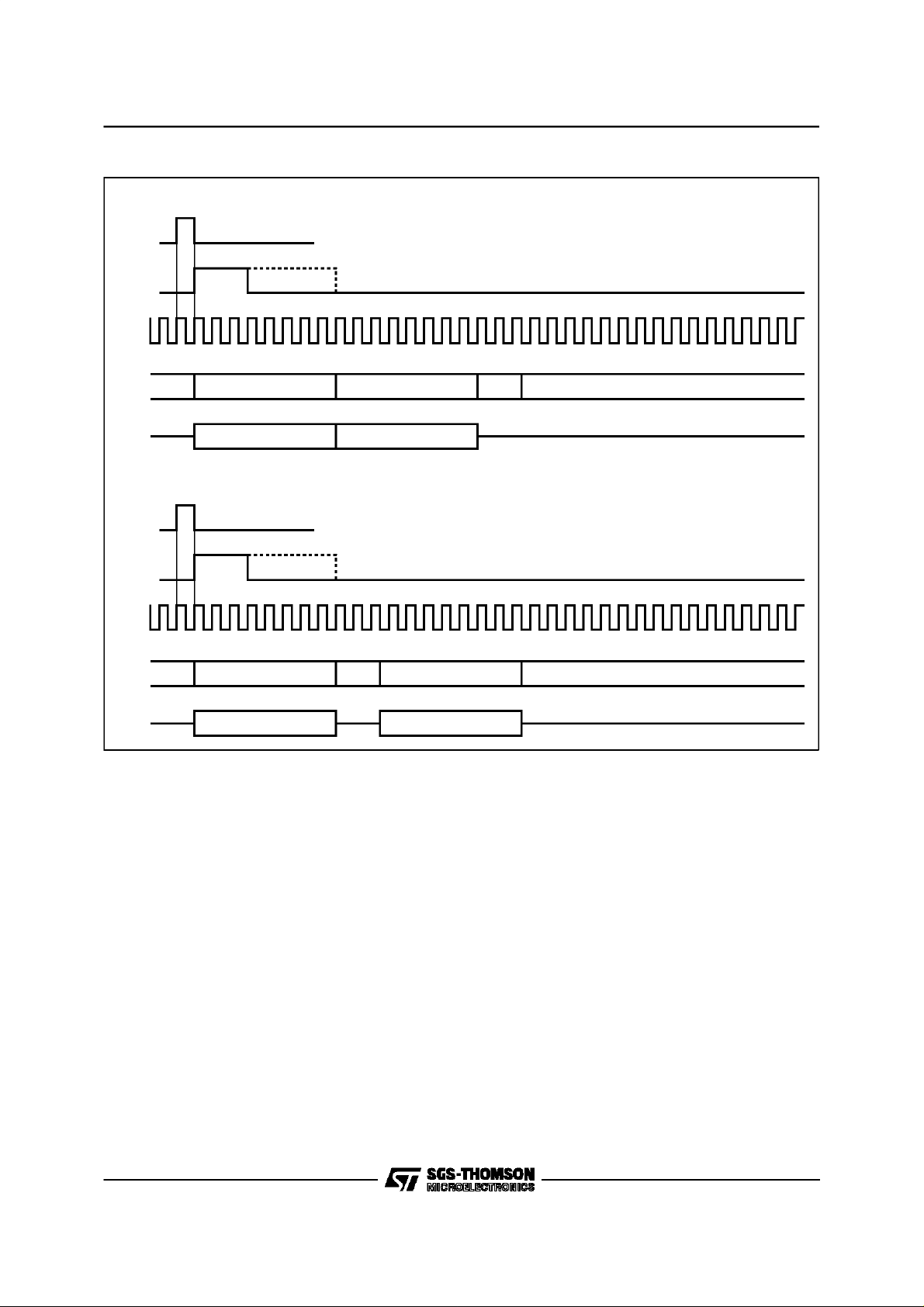
Figure1: Digital InterfaceFormat (*)
FORMAT 1
(delayed timing)F5
ST5090
F6
MCLK
DR
DX
F9
MCLK
DR
DX
FORMAT 2
(non delayed timing)
XB2B1 XX
B2B1
(delayed timing)F8
(non delayed timing)
XB2B1 XX
B2B1
D93TL075
(*) SignificantOnly ForCompanded Code.
propriate programmable register. CS- must return
high at the end of the 2nd byte.
To read-back status information from ST5090,the
first byte of the appropriate instruction is strobed
in during the first CS- pulse, as defined in Table
1. CS- must be set low for a further 8 CCLK cycles, during which data is shifted out of the CO
pin on the fallingedges of CCLK.
When CS- is high, CO pin is in the high impedance Tri-state, enabling CO pins of several devices to be multiplexedtogether.
Thus, to summarise, 2 byte READ and WRITE instructions may use either two 8-bit wide CSpulsesor a single16 bit wide CS- pulse.
I.8 Control channel access toPCM interface:
It is possible to access the B channel previously
selected in Register CR1 in the case of companded code only.
A byte written into Control Register CR3 will be
automatically transmitted from D
output in the
X
following frame in placeof the transmitPCMdata.
A byte written into Control Register CR2 will be
automatically sent through the receivepath to the
Receive amplifiers.
In orderto implementa continuous data flow from
the Control MICROWIRE interface to a B channel, it is necessary to send the control byte on
each PCM frame.
A current byte received on D
input can be read
R
in the register CR2. In order to implement a continuous data flow from a B channel to MICROWIRE interface,it is necessary to read register CR2 at each PCM frame.
7/29

ST5090
IIPROGRAMMABLE FUNCTIONS
For both formats of Digital Interface, programmable functions are configured by writing to a number of registersusing a 2-byte write cycle.
verification. Byte one is always register address,
while byte two isData.
Table 1 lists the register set and their respective
adresses.
Most of theseregisters can also be read-back for
Table 1: ProgrammableRegister Intructions
Function Address byte
76543210
Single byte Power up/down P X X X X X 0 X none
Write CR0 P 000001XseeCR0TABLE 2
Read-back CR0 P 0 0 0 0 1 1 X see CR0
Write CR1 P 000101XseeCR1TABLE 3
Read-back CR1 P 0 0 0 1 1 1 X see CR1
Write Data to receive path P 001001XseeCR2TABLE 4
Read datafrom D
Write Data to D
Write CR4 P 010001XseeCR4TABLE 6
Read-back CR4 P 0 1 0 0 1 1 X see CR4
Write CR5 P 010101XseeCR5TABLE 7
Read-back CR5 P 0 1 0 1 1 1 X see CR5
Write CR6 P 011001XseeCR6TABLE 8
Read-back CR6 P 0 1 1 0 1 1 X see CR6
Write CR7 P 011101XseeCR7TABLE 9
Read-back CR7 P 0 1 1 1 1 1 X see CR7
Write CR8 P 100001XseeCR8TABLE 10
Read-back CR8 P 1 0 0 0 1 1 X see CR8
Write CR9 P 100101XseeCR9TABLE 11
Read-back CR9 P 1 0 0 1 1 1 X see CR9
Write CR10 P 101001XseeCR10 TABLE 12
Read-back CR10 P 1 0 1 0 1 1 X see CR10
Write CR11 P 101101XseeCR11 TABLE 13
Read-back CR11 P 1 0 1 1 1 1 X see CR11
Write Test Register CR14 P 111001Xreserved
R
X
P001011XseeCR2
P001101XseeCR3TABLE 5
Data byte
NOTE 1: bit 7 ofthe addressbyte and data byteis always the firstbit clocked into orout from:CI and CO pins when MICROWIREserial
NOTE 2: ”P” bit isPower up/downControl bit. P = 1 MeansPower Down.
NOTE 3: Bit 2 is write/read selectbit.
NOTE 4: RegistersCR12, CR13, and CR15 are not accessible.
8/29
port isenabled.
X =reserved: write0
Bit 1 indicates, if set,the presence of a second byte.
Table 2: ControlRegister CR0Functions
ST5090
76543210
F1 F0 CM MA IA FF B7 DL
0
0
1
0
0
1
1
1
0
1
0
0
1
0
0
1
1
1
0
1
0
1
*: state at power on initialization
(1): significantin companded mode only
MCLK = 512 kHz
MCLK = 1.536 MHz
MCLK = 2.048 MHz
MCLK = 2.560 MHz
Linear code
Companded code
Linear Code Companded Code
2-complement *
sign and magnitude
2-complement
1-complement
B1 and B2 consecutive
B1 and B2 separated
8 bitstime-slot
7 bitstime-slot
01Normaloperation
Digital Loop-back
Function
*
*
MU-law: CCITT D3-D4 *
MU-law: Bare Coding
A-law including even bit inversion
A-law: Bare Coding
* (1)
(1)
* (1)
(1)
*
Table 3: ControlRegister CR1 Functions
76543210
DM1 DM0 DO MR MX EN TS SV
X
0
0
1
1
1
0
1
0
1
0
1
0
1
0
1
*: state at power on initialization
(1): significant in companded mode only
delayed data timing
non-delayed normal data timing
non-delayed reverse data timing
L0 latch set to 1
L0 latch set to 0
D
connected to rec. path
R
CR2 connected to rec. path
Trans path connected to D
CR3 connected to D
X
voice data transfer disable
voice data transfer enable
B1 channel selected
B2 channel selected
013.3V power supply
5.0V power supply
Function
X
*
*
*
(1)
*
(1)
*
* (1)
(1)
*
9/29
 Loading...