

SGS Thomson Microelectronics ST5088FN, ST5088D Datasheet
PROGRAMMABLE AUDIO FRONT END
FOR DIGITAL PHONES AND ISDN TERMINALS
FEATURES:
CompleteCODECandFILTERsystemincluding:
PCM ANALOG TO DIGITAL AND DIGITAL TO
ANALOG CONVERTERS
POWERFUL ANALOG FRONT END CAPABLE TO INTERFACEDIRECTLY:
- MicrophoneDynamic or Electrete
- Earpiecedownto 100Ω orup to150nF
- Loudspeakerdown to 50Ω or Buzzer up to
600nF.
TRANSMITBAND-PASSFILTER
ACTIVERC NOISE FILTER
RECEIVE LOW-PASS FILTER WITH SIN X/X
CORRECTION
MU-LAW OR A-LAW SELECTABLE COM-
PANDING CODER AND DECODER
PRECISIONVOLTAGE REFERENCE
Phones Features:
DUAL SWITCHABLE MICROPHONE AMPLIFIER INPUTS. GAIN PROGRAMMABLE: 15
dB RANGE,1 dB STEP.
LOUDSPEAKERAMPLIFIEROUTPUT.
SWITCHABLE MAXIMUM GAIN: +9dB/+27dB
WITH AUTOMATIC DIGITAL ANTICLIPPING
SYSTEM. aTTENUATION PROGRAMMABLE:
30dB RANGE,2dB STEP.
SEPARATEEARPIECE AMPLIFIEROUTPUT.
ATTENUATION PROGRAMMABLE: 15 dB
RANGE, 1 dB STEP.
AUXILIARY TAPE RECORDER ANALOG INTERFACE:Tx + Rx COMBINEDOUTPUT.
AUXILIARY SWITCHABLE EXTERNAL RING
INPUT (EAIN).
TRANSIENT SUPRESSION SIGNAL DURING
POWERON.
INTERNAL PROGRAMMABLE SIDETONE
CIRCUIT. ATTENUATION PROGRAMMABLE:
15 dB RANGE, 1 dB STEP, INDEPENDENT
FROM Rx CONTROL.
INTERNALRING OR TONE GENERATORINCLUDING DTMF TONES, SINEWAVE OR
SQUAREWAVE WAVEFORMS. ATTENUATION PROGRAMMABLE: 27 dB RANGE, 3
dB STEP.
RINGER CONTROL PROGRAMMABLE IN-
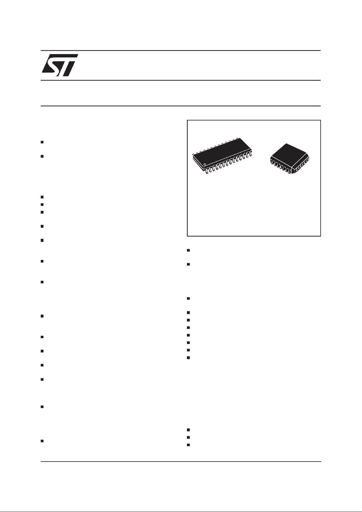
ST5088
PLCC28SO28
ORDERING NUMBERS:
ST5088D ST5088FN
TERNALLY(µP)OR EXTERNALLY(pin AT)
COMPATIBLE WITH HANDS-FREE CIRCUIT
TEA7540.
ON CHIP SWITCHABLE ANTI-ACOUSTIC
FEED-BACKCIRCUIT (ANTI-LARSEN).
GeneralFeatures:
EXTENDED TEMPERATURE RANGE OPERATION
EXTENDEDPOWERSUPPLYRANGE5V±10%.
60 mW OPERATINGPOWER(TYPICAL).
1.0 mW STANDBYPOWER (TYPICAL).
CMOSDIGITAL INTERFACES.
SINGLE + 5V SUPPLY.
DIGITALLOOPBACKTEST MODE.
PROGRAMMABLE DIGITAL AND CONTROL
INTERFACES:
–Digital PCM Interface associated with
separate serial Control Interface MICROWIRE compatible.
–GCI interfacecompatible.
(*) Functionality guaranteed in the range – 25°C to +85°C;
Timingand ElectricalSpecificationsare guaranteed in the range
–5°C to +70°C.
APPLICATIONS:
ISDN TERMINALS.
DIGITALTELEPHONES
CT2 AND GSM APPLICATIONS
–25°C TO +85°C.
(*)
December 1999
This is advanced information on a new product now in development or undergoing evaluation. Details are subject to change without notice.
1/33

ST5088
PIN CONNECTION (Topview)
HFI
HFO
VFR+
VFR-
VCC
LS-
LS+
GND
MS CS-/A3
DX CCLK/A0
AT
CO/A2
CI/A1 MCLK
2
3
4
5
6
7
8
9
10
12
13
BLOCK DIAGRAM
SO28
D93TL047
28
27
26
25
24
23
22
21
20
19
18
17
16
1514DR FS
EAIN1
GNDA
MIC 2VCCA
TRO
MIC 1MIC 1+
MIC 2+
N.C.11
LO
PLCC28
2/33
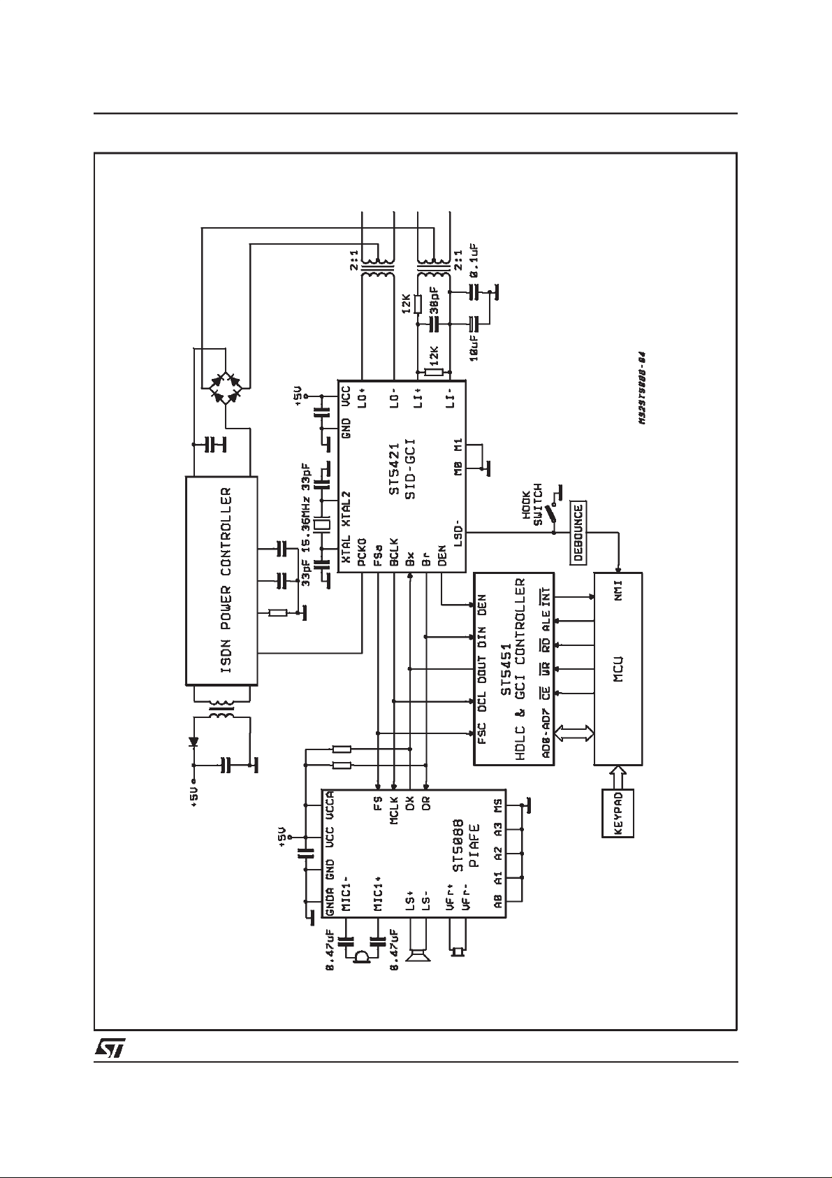
TYPICALISDN TELEPHONE SET APPLICATION
ST5088
3/33
ST5088
GENERAL DESCRIPTION
ST5088 PIAFE is a combined PCM CODEC/FILTERdeviceoptimizedfor ISDNTerminalsand Digital Telephone applications. This device is A-law
and Mu-lawselectable and offers a number ofprogrammable functions accessed through a serial
controlchannel.
Depending on mode selected, channel control is
provided by means of a separate serial channel
control MICROWIRE compatible or multiplexed
with the PCM voice data channel in a GCI compatible format requiring only 4 digital interface
pins. When separate serial control interfaceis selected, PCM interface is compatible with Combo I
and Combo II families of devices such as
ETC5057/54,TS5070/71.
PIAFE is built using SGS-THOMSON’s advanced
HCMOS process.
Transmitsection of PIAFE consists of an amplifier
with switchable high impedance inputs followed
by a programmable gain amplifier, an active RC
antialiasingpre-filter to provideattenuationof high
frequency noise, an 8th order switched capacitor
band pass transmit filter and an A-law/Mu-law selectable compandigencoder.
Receive section consist of an A-law/Mu-law selectable expanding decoder which reconstructs
the analog sampled data signal, a 3400 Hz low
pass filter with sin X/X correction followed by two
separate programmable attenuation blocks and
two power amplifiers: one can be used to drive an
earpiece, and the other to drive a 50 Ω loud-
speakeror a piezo transducerup to 600nF.
When the loudspeaker section is set up with
maximum gain (+27dB) the device provide internally a programmable digital anticlipping system
to avoid output distortion.
Programmable functions on PIAFE include a
Ring/Tone generator which provides one or two
tones and can be directed to earpiece or to loudspeaker(or buzzer).
A simple ringer control interface can bypass µP
control of sweep frequency and ring ON/OFF
phases.
A separate programmable gain amplifier allows
gain control of the signal injected. Ring/Tone generator provides sinewave or squarewave signal
with precise frequencies which may be also directed to the input of the Transmit amplifier for
DTMF tone generation.
An auxiliary analog input (EAIN) is also provided
to enable for example the output of an external
band limited Ring signal to the Loudspeaker.
Transmit signal may be fed back into the receive
ampifier with a programmable attenuation to provide a sidetonecircuitry.
A switchable anti-accoustic feed-back system
cancelsthe larsen effect in speech monitoring application.
Two additional pins are provided for insertion of
an external Handfree functionin the Loudspeaker
receivepath.
An output latch controlled by register programming permits external device control.
PIN FUNCTIONS
SO
1,2 1,2 HFI, HFO Hands free I/Os:
3,4 3,4 V
55 V
6,7 6,7 LS-,LS+ Receive analog loudspeaker amplifier complementary outputs,
4/33
PLCC
Name Description
Thesetwopins canbe usedtoinsert an externalHandfreecircuit
suchasthe TEA7540in thereceivepath.HFOisanoutput which
providesthesignalissuedfromoutput ofthe receive low pass filter
whileHFIis a highimpendance input whichis connected directly to
oneof theinputs ofthe Loudspeaker amplifier.
Fr+,VFr–
CC
Receive analog earpiece amplifier complementary
outputs, capable of driving load impedances between 100
and 400 Ω or a piezo ceramic t ransducer up to 150nF.
These outputs can drive directly earpiece transductor. The
signal at this output can drive be the summ of:
- Receive Speech signal from D
- Internal Tone Generator,
- Sidetone signal.
Positive power supply input for the digital section. +5 V + 10%.
intended for driving a Loudspeaker: 80 mW on 50Ω load
impedance can be provided at low distorsion meeting
specifications.
Alternatively this stage can drive a piezo transducer up to
600nF. The signal at these outputs can be the sum of:
- Receive Speech signal from D
- Internal Tone generator,
- External input signal from EAIN input.
,
R
,
R

PIN FUNCTIONS (continued)
ST5088
SO
PLCC
Name Description
8 8,9 GND Ground: All digital signals are referenced to this pin.
9 10 MS Mode Select: This input selects COMBO I/II interface mode
with separate MICROWIRE Control interface when tied high
and GCI mode when tied low.
10 11 D
X
Transmit Data ouput: Data is shifted out on this pin during the
assigned transmit time slots. Elsewhere D
output is in the
X
high impendance state. In COMBO I/II mode, voice data byte
is shifted out from TRISTATE output D
at the MCLK
X
frequency on the rising edge of MCLK. In GCI mode, voice
data byte and control bytes are shifted out from OPEN-DRAIN
output D
at half the MCLK. An external pull up resistor is
X
needed.
11 12 AT Alternate Tone: Ring frequency out is controlled without µP
intervention. Tri-state logic controls: f1 (Vcc), f2 (GND), pause
(High Impedance).
14 15 D
R
Receive data input: Data is shifted in during the assigned
Received time slots. In the COMBO I/II mode, voice data byte
is shifted in at the MCLK frequency on the falling edges of
MCLK. In the GCI mode, PCM data byte and contol byte are
shifted in at half the MCLK frequency on the receive rising
edges of MCLK.There is one period delay between transmit
rising edge and receive rising edge of MCLK.
15 16 FS Frame Sync input: This signal is a 8kHz clock which defines
the start of the transmit and receive frames. Either of three
formats may be used for this signal: non delayed timing mode,
delayed timing and GCI compatible timing mode.
16 17 MCLK Master Clock Input: This signal is used by the switched
capacitor filters and the encoder/decoder sequencing logic.
Values must be 512 kHz, 1.536 MHz, 2.048 MHz or 2.56 MHz
selected by means of Control Register CRO. MCLK is used
also to shift-in and out data. In GCI mode, 2.56 MHz and 512
kHz are not allowed.
17 18 LO Open drain output:
a logic 1 written into DO (CR1) appears at LO pin as a logic 0
a logic 0 written into DO puts LO pin in high impedance.
18 – N. C. No connected.
21 22 MIC2+ Alternative positive high impedance input to transmit pre-
amplifier.
22 23 MIC1+ Positive high impedance input to transmit pre-amplifier for
microphone symetrical connection.
23 24 MIC1- Negative high impedance input to transmit pre-amplifier for
microphone symetrical connection.
24 21 TRO Tape Recorder Output: This pin provides the analog
combination of Tx voice signal and Rx voice signal.
25 25 V
CCA
Positive power supply input for the analog section.
+5 V + 10%. V
CC
and V
must be directly connected
CCA
together .
26 26 MIC2- Alternative negative high impedance input to transmit pre-
amplifier.
27 27 GNDA Analog Ground: All analog signals are referenced to this pin.
GND and GNDA must be connected together close to the
device.
28 28 EAIN ExternalAuxiliary input: This input can be used to provide
alternate signals to the Loudspeaker in place of Internal Ring
generator. Input signal should be voice band limited.
5/33
ST5088
Following pin definitions are used only when COMBO I/II mode with separate MICROWIRE compatible serial control port is selected. (MS inputset equal one)
PIN FUNCTIONS (continued)
SO
12 13 CO Control data Output: Serial control/status information is shifted
13 14 CI Control data Input:SerialControl information is shiftedintothe
19 19 CCLK Control Clock input: This clock shifts serial control information
20 20 CS- Chip Select input: When this pin is low, control information is
PLCC
Name Description
out from the PIAFE on this pin when CS- is low on the falling
odges of CCLK.
PIAFEon thispin when CS- islow on the rising edges of CCLK.
into CI and out from CO when the CS- input is low, depending
on the current instruction. CCLK may be asynchronous with
the other system clocks.
written into and out from the PIAFE via CI and CO pins.
Followingpin definitions are used only when the GCI mode is selected.(MS input set equal zero)
PIN FUNCTIONS (continued)
SO
19,13,12,20 19,14,13,20 A0,A1,A2,A3 These pins select the address of PIAFE on GCI interface and
PLCC
FUNCTIONAL DESCRIPTION
Power on initialization:
When power is first applied, power on reset
cicuitryinitializes PIAFE and puts it into the power
Name Description
must be hardwired to either V
C4,C5,C6,C7 bits of the first address byte respectively.
or GND. A0,A1,A2,A3 refer to
CC
When a power up command is given, all de-activated circuits are activated, but output D
main in the high impedance state on B time slots
until the second Fs pulse after power up, even if a
B channel is selected.
will re-
X
down state. Gain Control Registersfor the various
programmable gain amplifiers and programmable
switches are initialized as indicated in the Control
Register description section. All CODEC functions
are disabled.Digital Interface is configuredin GCI
mode or in COMBOI/II mode dependingon Mode
Select pin connection.
The desired selection for all programmable functions may be intialized prior to a power up command using Monitor channel in GCI mode or MICROWIREport in COMBOI/II mode.
Power down state:
Following a period of activity, power down state
may be reentered by writing a power down instruction.
ControlRegisters remain in their current state and
can be changedeither by MICROWIREcontrol interface or GCI control channel depending on
modeselected.
In addition to the power down instruction, detection of loss MCLK (no transition detected) automatically enters the device in ”reset” power down
Power up/down control:
Following power-on initialization, power up and
state with D
output in the high impedance state
X
and L0 in high impedancestate.
power down control may be accomplishedby writing any of the control instructions listed in Table 1
into PIAFE with ”P” bit set to 0 for power up or 1
for power down.
Normally, it is recommended that all programmable functions be initially programmed while the
device is powered down. Power state control can
then be included with the last programming instruction or in a separatesingle byte instruction.
Any of the programmable registers may also be
modified while ST5088 is powered up ordown by
setting ”P” bit as indicated. When power up or
down control is entered as a single byte instruction, bit 1 must be set to a 0.
Transmitsection:
Transmit analog interface is designed in two
stages to enable gains up to 35 dB to be realized.
Stage 1 is a low noise differential amplifierprovid-
ing 20 dB gain. A microphone may be ca-
pacitevely connected to MIC1+, MIC1- inputs,
while the MIC2+ MIC2– inputs may be used to
capacitively connect a second microphone (for
digital handsfree operation) or an auxiliary audio
circuitsuch as TEA 7540 Hands-free circuit. MIC1
or MIC2 source is selected with bit 7 of register
CR4.
Following the first stage is a programmable gain
6/33

ST5088
amplifier which provides from 0 to 15 dB of additional gain in 1 dB step. The total transmit gain
should be adjusted so that, at reference point A,
see Block Diagram description, the internal 0
dBmO voltage is 0.739 V (overload level is 1.06
Vrms). Second stage amplifier can be programmed with bits 4 to 7 of CR5. To temporarily
mute the transmit input, bit TE (6 of CR4) may be
set low. In this case, the analog transmit signal is
grounded and the sidetonepath is also disabled.
An activeRC prefilterthenprecedes the 8th order
band pass switched capacitor filter. A/D converter
has a compressing characteristic according to
CCITT A or mu255 coding laws, which must be
selected by setting bits MA, IA in register CR0. A
precision on chip voltage reference ensuresaccurate and highly stabletransmission levels.
Any offset voltage arising in the gain-set amplifier,
the filtersor the comparatoris cancelled by an internalautozero circuit.
Each encode cycle begins immediatly at the beginning of theselected Transmit time slot. The total signal delay referenced to the start of thetime
slot is approximatively195 µs (due to the transmit
filter) plus 123 µs (due to encoding delay), which
totals 320 µs. Voice data is shifted out on D
X
during the selected time slot on the transmit rising
adges of MCLK.
Receive section:
Voice Data is shifted into the decoder’s Receive
voice data Register via the D
pin during the se-
R
lected time slot on the 8 receiveedges of MCLK.
The decoder consists of an expandingDAC with
either A or MU255 law decoding characteristic
which is selected by the same control instruction
used to select the Encode law during intitialization. Following the Decoder is a 3400 Hz 6th order low pass switched capacitorfilter with integral
Sin X/X correctionfor the 8 kHz sample and hold.
0 dBmO voltage at this (B) reference point (see
Block Diagram description) is 0.49 Vrms. A transcient suppressing circuitry ensure interference
noise suppressionat power up.
The analog speech signal output can be routed
either to earpiece (V
FR+,VFR-
outputs) or to loudspeaker (LS+, LS- outputs) by setting bits SL and
SE (1and 0 of CR4).
Total signal delay is approximatively190 µs (filter
plus decoding delay) plus 62.5 µs (1/2 frame)
which gives approximatively252 µs.
Differential outputs V
FR+,VFR-
are intended to directly drive an earpiece. Preceding the outputs is
a programmableattenuationamplifier, which must
be set by writing to bits 4 to 7 in register CR6. Attenuationsin the range 0 to -15 dB relativeto the
maximum level in 1 dB step can be programmed.
The input of this programmable amplifier is the
summ of several signals which can be selected
by writing to register CR4.:
- Receive speech signal which has been decodedand filtered,
- Internally generated tone signal, (Tone amplitude is programmed with bits 4 to 7 of register
CR7),
- Sidetone signal, the amplitude of which is programmedwith bits 0 to 3 of registerCR5
V
FR+
andV
outputsarecapableof drivingoutput
FR-
power level up to 14mW into differentially connectedloadimpedancebetween100 and 400Ω.
Differential outputs LS+,LS- are intended to directly drive a Loudspeaker.Preceding the outputs
is a programmable attenuation amplifier, which
must be set by writing to bits 0 to 3 in register
CR6. Attenuations in the range 0 to -30 dB relative to the maximum level in 2.0 dB step can be
programmed.The input of this programmableamplifier can be the summ of signals which can be
selectedby writing to register CR4:
- Receive speech signal which has been decodedand filtered,
- Internally generated tone signal, (Tone amplitude is programmed with bits 4 to 7 of register
CR7),
- EAIN input which may be an alternate Ring
signal or any voice frequency band limited
signal. (An external decoupling capacitor of
about0.1µF is necessary).
Receive voice signal may be directed to output
HFO by means of bit HFE in Register CR4. After
processing, signal must be re-enteredthrough input HFI to Loudspeakeramplifier input. (An external decoupling capacitor of about 0.1µF is necessary).
The output loudspeaker section has two switchable gains of +9dB and +27dB.
+9dB LS Gain
This gain mode is fully equivalent to PIAFE
ST5080 behaviour.
LS+ and LS- outputs are capableof driving output
power level up to 80 mW into 50Ωdifferentially
connectedload impedance at low distortion meeting PCM channel specifications. When the signal
source is a Ring squarewavesignal, power levels
up to approximatively200 mW can be delivered.
+27dBLS Gain
Additional gain of 18dB has the purpose to increase the undistorted output power up to
150mW typical with digital input DR ranging from
-12dBm0to +3dBm0.
Output DC offset is limited by high pass filter with
35Hz cut frequency (wit h LS gain = +9dB cut frequency = 9Hz)
Anti-acoustic feed-back for loudspeakerto handset microphone loop with squelch effect: on chip
7/33

ST5088
switchable anti-larsen for loudspeaker to handset
microphone feedback is implemented. A 12dB
depth gain control on both transmit and receive
path is provided to keep constant the loop gain.
On the transmit path the 12dB gain control is provided starting from the CR5 transmit gain definition; at the same time, on the receive path the
12dB gain control is provided starting from CR6
receive gain definition.
DIGITAL ANTICLIPPINGSYSTEM(D.A.S.)
An automatic anticlipping system is necessary to
avoid distortion on LS+/LS- when the output
swing approaches the supply rails. (LS GAIN >>
+9dB).
The digital anticlipping system calculates equivalent input signal on DR pin and compares it with a
selectable anticlipping threshold. The D.A.S. is
then able to reduce the overall gain in order to
avoid or limit the distortion.
Four different thresholds are programmable via
register:
-15dBm0 D < 1% For safe margin
-13dBm0 D = 1% For normal operation
-9dBm0 D ≥ 1% Fornoisy ambient (*)
-7dBm0 D >> 1% For very noisy ambient (*)
(*) When environment is noisy, power output
might be more important than 1% distortion.
Gain reduction of the D.A.S. (Anticlipping Attack)
has a fixedspeed of 8KHz.
Gain recovery or increase (Anticlipping Release)
has 4 programmable speeds of 4Hz, 8Hz, 31Hz
and 62Hz.
TAPE RECORDEROUTPUT(TRO)
This section provides a combinationof Txand Rx
Analog Signals to an external user like a recordering machine. The output levels relative to a
signal of 0dBm0 on channel Dx and DR are:
Rx TRO= 0.245V
Tx TRO = 0.246V
(for0dBm0 on DR)
RMS
(for0dBm0 on DX)
RMS
The single ended Op Amp is able to drive an externalload as low as 600Ω.
ALTERNATE TONE CONTROL(AT)
This section allows to simplifythe microprocessor
control of ringeroperation. When pin AT is put externally at high impedance state (or left open) the
control of ring frequency emission is totally
through a microprocessor, which updates in real
time the contents of various registers.
When pin AT is forced at GND or Vcc the ring
generator emits respectively the frequencies f2
(GND) and f1 (Vcc), previously defined through
registers CR9 (f2) and CR8(f1). This operative
mode requires only start-up interventionof the mi-
croprocessor.
Digitaland Control Interface:
PIAFE provides a choice of either of two types of
Digital Interface for both control data and PCM.
For compatibilitywith systems which use time slot
oriented PCM busses with a separate Control Interface, as used on COMBO I/II families of devices, PIAFE functions are describedin next section.
Alternatively, for systems in which PCM and control data are multiplexedtogether using GCI interface scheme, PIAFE functions are described in
the section following the next one.
PIAFE will automatically switch to one of these
two types of interfaceby sensingthe MS pin.
Due to Line Transceiver clock recovery circuitry,a
low jitter may be provided on F
clocks. F
and MCLK must be always in phase.
S
and MCLK
S
For ST5421S Transceiver, as an example,
maximun value of jitter amplitude is a step of 65
ns at each GCI frame (125µs). So, the maximum
jitter amplitude is 130 ns pk-pk.
COMBOI/II mode.
DigitalInterface (Fig. 1)
F
Frame Sync input determines the beginningof
S
frame. It may have any duration from a single cycle of MCLK to a squarewave.Two different relationships may be establishedbetween the Frame
Sync input and the first time slot of frame by setting bit 3 in register CR0. Non delayed data mode
is similar to long frame timing on ETC5057/
TS5070 series of devices (COMBO I and
COMBO II respectively): first time slot begins
nominally coincident with the rising edge of F
S
Alternative is to use delayed data mode, which is
similar to short frame sync timing on COMBO I or
COMBO II, in which F
inputmust be high at least
S
a half cycle of MCLK earlier the frame beginning.
A time slot assignment circuit on chip may be
used with both timing modes, allowing connection
to one of the two B1 and B2 voice data channels.
Two data formats are available: in Format 1, time
slot B1 corresponds to the 8 MCLK cycles following immediately the rising edge of FS, while time
slot B2 corresponds to the 8 MCLK cycles following immediately time slot B1.
In Format 2, time slot B1 is identical to Format 1.
Time slot B2 appears two bit slots after time slot
B1. This two bits space is left available for insertion of the D channel data.
Data format is selected by bit FF (2) in register
CR0. Time slot B1 or B2 is selected by bit T0 (0)
in Control Register CR1.
Bit EN (2) in control register CR1 enables or disables the voice data transfer on D
and DRas
X
appropriate. During the assigned time slot, D
.
X
8/33
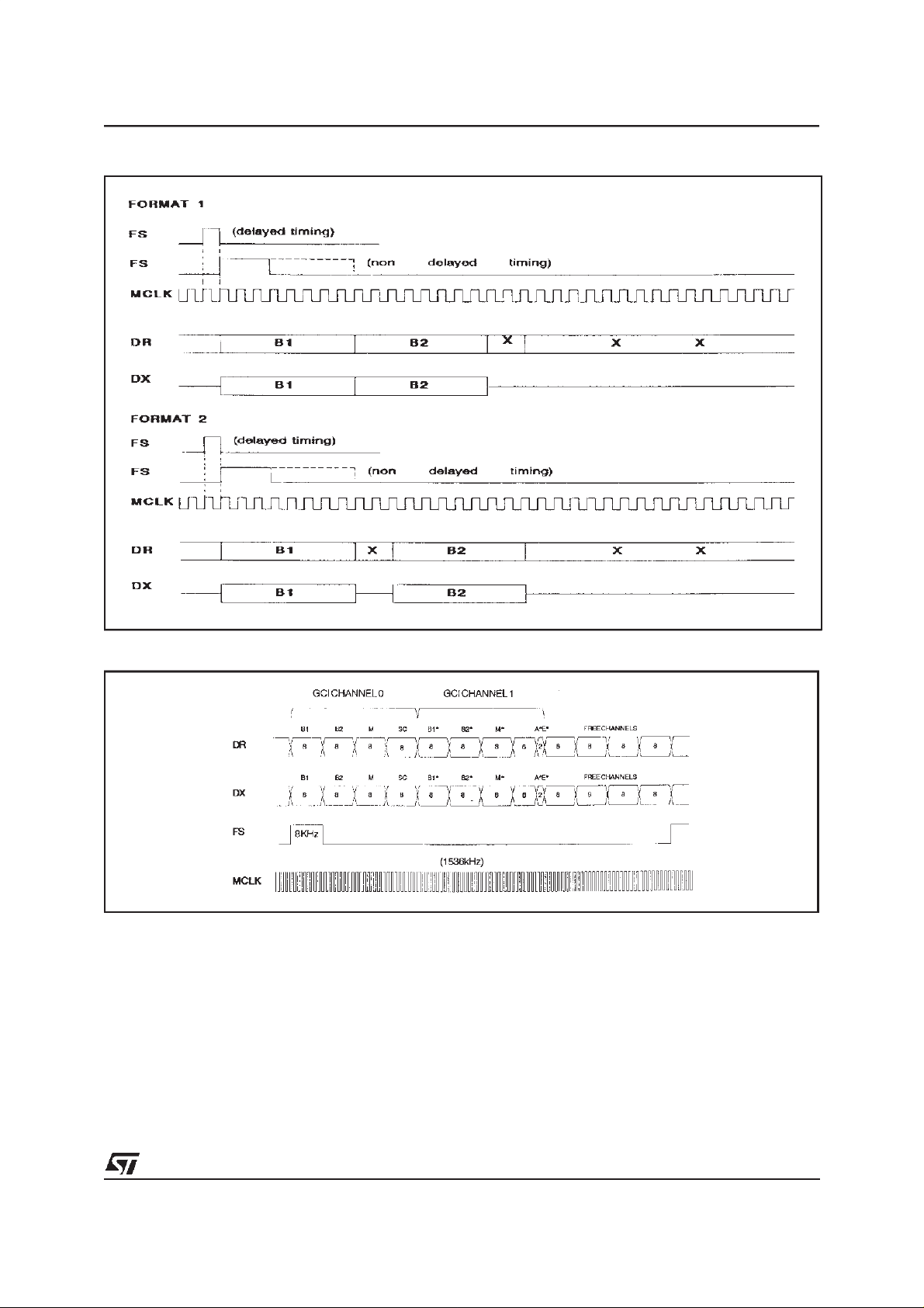
Figure 1: Digital Interface Format
ST5088
Figure 2: GCI InterfaceFrame Structure
output shifts data out from the voice data register
on the rising edges of MCLK. Serial voice data is
shifted into D
input during the same time slot on
R
the falling edges of MCLK.
D
is in the high impedance Tristate condition
X
when in the non selectedtime slots.
ControlInterface:
Control informationor data is written into or readback from PIAFE via the serial control port consisting of control clock CCLK, serial data input CI
and output CO, and Chip Select input, CS-. All
control instructionsrequire 2 bytes as listed in Ta-
ble 1, with the exception of a single byte powerup/down command.
To shift control data into ST5088, CCLK must be
pulsed high 8 times while CS- is low. Data on CI
input is shifted into the serial input registeron the
rising edge of each CCLK pulse. After all data is
shifted in, the content of the input shift register is
decoded, and may indicate that a 2nd byte of
control data will follow. This second byte may
either be defined by a second byte-wide CSpulse or may follow the first contiguously, i.e. it is
not mandatory for CS- to return high in between
the first and second control bytes. At the end of
9/33

ST5088
the 2nd control byte, data is loaded into the appropriate programmable register. CS- must return
high at the endof the 2nd byte.
To read-back status information from PIAFE, the
first byte of the appropriate instruction is strobed
in during the first CS- pulse, as defined in Table
1. CS- must be set low for a further 8 CCLK cycles, during which data is shifted out of the CO
pin onthe falling edges of CCLK.
When CS- is high, CO pin is in the high impedance Tri-state, enabling CO pins of several devices to be multiplexedtogether.
Thus, to summarise,2 byte READ and WRITE instructions may use either two 8-bit wide CSpulses or a single16 bit wide CS-pulse.
Controlchannel access to PCM interface:
It is possible to access the B channel previously
selected in Register CR1.
A byte written into Control Register CR3 will be
automatically transmitted from D
output in the
X
followingframe in place of the transmit PCM data.
A byte written into Control Register CR2 will be
automatically sent through the receive path to the
Receiveamplifiers.
In order to implement a continuousdata flow from
the Control MICROWIRE interface to a B channel, it is necessary to send the control byte on
each PCM frame.
A current byte received on D
input can be read
R
in the register CR2. In order to implement a continuous data flow from a B channel to MICROWIREinterface, it is necessary to read register CR2 at each PCM frame.
GCI COMPATIBLEMODE
GCI interface is an European standardized interface to connect ISDN dedicated components in
the different configurations of equipment as Terminals, NetworkTerminations,PBX, etc...
In a Terminal equipment, this interface called
SCIT for SpecialCircuit Interface for Terminals allows for exampleconnection between:
- ST5421 (SID-GCI) and ST5451 (HDLC/GCI
controller)used for 16 kbit/s D channel packet
framesprocessingand SID control,
- Peripheraldevices connected to a 64 kbit/s B
channel and ST5451 used for GCI peripheral
control.
ST5088 may be assigned to one of the B channels present on the GCI interface and is monitored via a control channel which is multiplexed
with the 64 kbit/sVoice Data channels.
Figure 2 shows the frame structure at the GCI interface. Two 256 kbit/s channel are supported.
a)GCI channel 0: It is structured in four sub-
channels:
–B1 channel 8 bits per frame
–B2 channel 8 bits per frame
–M channel8 bitsperfra m eignoredbyPIAFE
–SC channel 8 bits per frame ignored by
PIAFE
Only B1 or B2 channelcan be selected in
PIAFEfor PCM data transfer.
b)GCI channel 1: It is structured also in four
subchannels:
–B1* channel 8 bits per frame
–B2* channel 8 bits per frame
–M* channel 8 bitsper frame
–SC* which is structuredas follows:
6 bits ignored by PIAFE
A* bit associatedwith M* channel
E* bit associatedwith M* channel.
B1*or B2* channel can be selectedin PIAFE
for PCM data transfer.
M*channel and twoassociated bitsE* and A*
areused for PIAFEcontrol.
Thus, to summarize, B1, B2, B1* or B2* channel
can be selected to transmit PCM data and M*
channel is used toread/write status/commandperipheral device registers. Protocol for byte exchange on the M* channel usesE* and A* bits.
Physical Interface
The interfaceis physically constitued with 4 wires:
InputData wire: D
OutputData wire: D
R
X
Bit Clock: MCLK
Frame Synchronization: F
S
Data is synchronized by MCLK and FSclock inputs.
F
insures reinitialization of time slot counter at
S
each frame beginning. The rising edge or FS is
the referencetime for the first GCI channel bit.
Data is transmitted in both directions at half the
MCLK input frequency. Data is transmitted on the
the rising edge of MCLK and is sampled one period after the transmit rising edge, also on a rising
edge.
Note: Transmit data may be sampled by far-end
device ie SID ST5421 on the falling edge 1.5 period afterthetransmit rising edge.
Unused channel are high impedance. Data outputs are OPEN-DRAIN and need an external pull
up resistor.
COMBOactivation/deactivation
ST5088 is automatically set in power down mode
when GCI clocks are idle. GCI section is reactivated when GCI clocks are detected. PIAFE is
completly reactivated after receiving of a power
up command.
Exchangeprotocol on M* channel
10/33
 Loading...