


ST486DX SMM
PROGRAMMING MANUAL
1stEDITION
NOVEMBER 1994

1. SMM OVERVIEW Pages 9
1.1 Introduction . . ............................................ 9
1.2 SGSThomson SMM Features . . . . . . . . . . . . . . . . . . . . . . . . ............ 9
1.3 ATypical SMM Routine . . . . . . . . . . . . . . . . . . . . . . . . . ..............10
2. SGS THOMSONSMM IMPLEMENTATION 13
2.1 HardwareBackground . . . . . . . . . . . . . . . . . . . . . . . . . . .............. 13
2.2 Configuration Control Registers . . . . . . . . . .......................... 14
2.3 SMMInstruction Summary . . . . . . . . . . . . . . . . ......................18
3. SMM SOFTWARECONSIDERATIONS 23
3.1 EnablingSMM . . ....................................... ... 23
3.2 SMM Handler Entry State . . . . . . . . . . . . . . . . . . . . . . ................ 24
3.3 Maintainingthe CPU State . . . . . . . . . . . . .......................... 28
3.4 Initializingthe SMM Environment . . . . . . . . . . . . . . . . . . . . . . . . ..........31
3.5 AccessingMain Memory Overlappedby SMM Memory . . . . .................. 32
3.6 I/ORestart . . . . . . . . . . . . . . . . . . . . . . ........................ 33
3.7 I/OPort Shadowing and Emulation . . . . . . . . . . . . . . . . . . . . . . . . . ........ 34
3.8 Returnto HLT Instruction . . . . . . . . . . . . . . . . . . . . . . ................ 35
3.9 Exitingthe SMI Handler . . . .................................... 37
3.10 Testing and DebuggingSMM Code . . . ..............................38
4. POWER MANAGEMENT FEATURES 41
4.1 Reducingthe Clock Frequency . . . . . . . . . . .......................... 41
4.2 Loweringthe CPU Supply Voltage . . . . . . . . . . . . . . . . . . . . .............. 41
4.3 SuspendMode . . . . ........................................ 42
Appendix A Assembler Macros for SGS Thomson Instructions 45
GENERAL INDEX
5

1. SMM OVERVIEW
1.1 Introduction
This Programmer’s Guide has been written to aidprogrammers in the creation of software using the
SGS-ThomsonSystem Management Mode (SMM)for ST486DX CPUs. This guide shouldbe
used in conjunctionwith the SGS-ThomsonST486DX and ST486DX2 Processors Data Book.
SMM programming related to the ST486SLC/eis covered in the ST486SLC/e SMM Programmer’s
Guide.
SMM provides the system designer withanother processor operating mode. Withinthis document
the standard x86 operating modes (real, v86and protected) are referred to as normal mode. Normal mode operation can be interrupted by an SMI interrupt orspecial instructionthatplaces the
processorin System Management Mode (SMM). SMM can beused to enhance the functionality of
the systemby providing power management,register shadowing,peripheral emulationand other
system level functions. SMM can be totally transparentto all application software, including protected mode operating systems.
1.2 SGS-ThomsonSMM Features
SMM operation within one of the SGS-Thomson ST486DX microprocessors is similar to related
operations performed by other x86 microprocessors. All processorswith SMM capability, switch
into real mode upon entry into the SMM interrupt handler. Each CPU has a unique SMM codelocations. However, theSMM memoryregion for the SGS-Thomson CPU has aprogrammable location and size. All devices save some of the CPU registers upon entry to SMM. The SGS-Thomson
CPU automatically saves minimalregister information reducing the entry andexit clock count to as
low as 100 clock cycles. Thiscompareswith Intel’s clock overhead for a typical entry and exitof
633 clock cycles. TheSGS-Thomson SMM implementationprovides unique instructionsthat save
additionalsegment registers as required by the programmer. The x86 MOV instruction can be used
to save the general purpose registers.
Althoughall SMMcapable CPUs provide I/O trapping, the SGS-Thomson CPUs simplify I/O type
identification and instruction restarting. SGS-ThomsonCPUs also make available to the SMM routine informationwhich can simplifyperipheral register shadowing.
SGS-Thomsonprovides a method to preventSMM configurationregisters from being accessed by
applications. Accessto the SMM configuration can be preventedby setting a bit in the CPU configuration space. Not allowing an application to disable or alter SMM operation is usefulfor antivirus or security measures.
ST486DX - SMM OVERVIEW
9
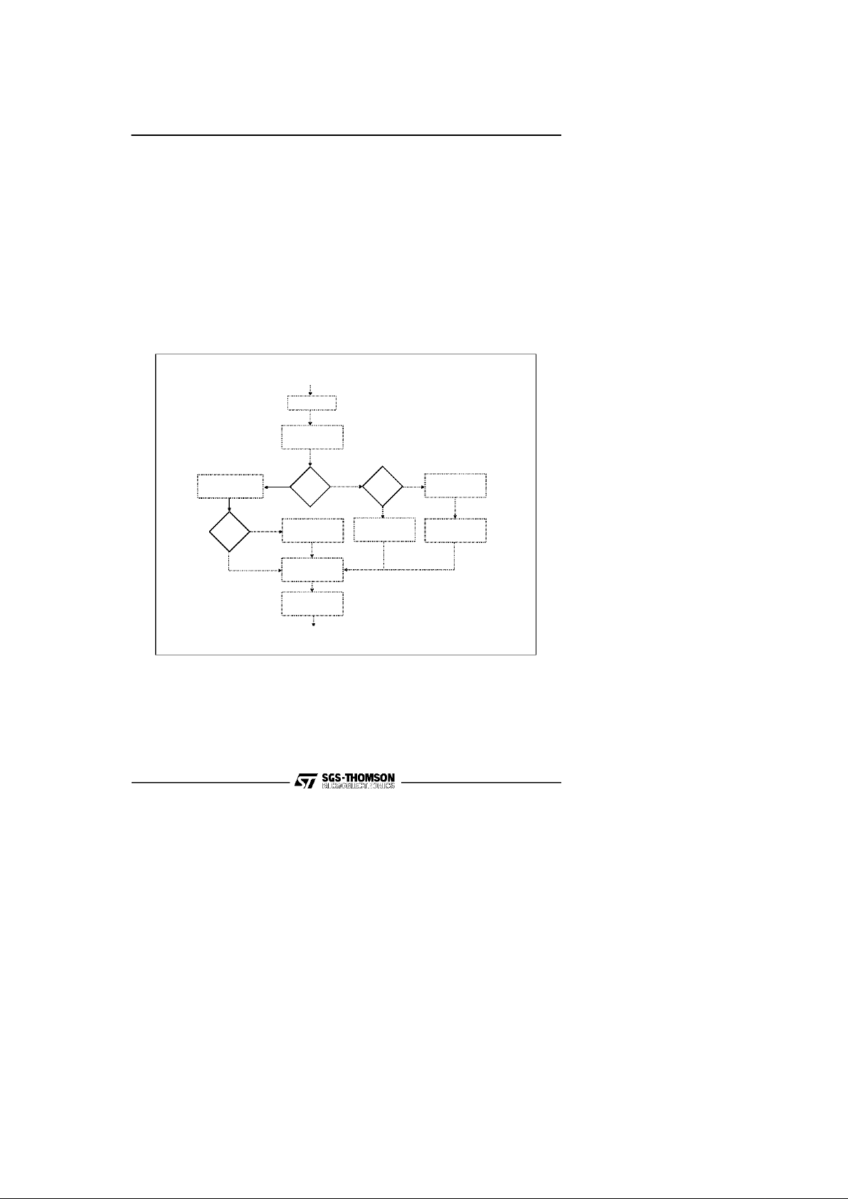
Figure 1 - 1. TypicalSMM Routine
SMM Entry
Save State
Initialize SMM
Environment
Trap?
Service
Non-Trap SMI
HALT?
Decrement
EIP
Device
OFF?
Shadow
Service
Trap SMI
Modify State
For I/O Restart
Restore
State
Resume
I/O
SMMExit
N
Y
Y
Y
N
N
or Emulate
1727400
ST486DX - SMMOVERVIEW
10
1.3 TypicalSMM Routines
A typical SMM routine is illustrated in the flowchart shown in Figure1-1. Upon entry to SMM,
the CPU registers that will be used by the SMM routine, must be saved. TheSMM environment is
initialized by setting up an Interrupt Descriptor Table,initializing segment limits and setting up a
stack. If the SMI wasa resultof an I/O bus cycle, the SMM routine can monitor peripheral activity, shadowread-only ports ,and/or emulate peripherals in software. If a peripheral was powered
down, the SMM routine can power up a peripheral and reissue theI/O instruction. If the SMI was
not caused by an I/O bus cycle, non-trap SMI functionscan be serviced. Ifthe instruction executing, when an SMI occurred,wasa HLT instruction, the HLT instructionit should be restarted when
the SMM routine is complete. Beforenormal operation is resumed,any CPU registers modified
during the SMM routine must be restored to their previous state.

2. SGS-ThomsonSMM IMPLEMENTATION
2.1 Hardware Background
2.1.1 SMM Pins
The signals at the SMI# and SMADS# pins are used to implement SMM. The SMI# pin is bi-directional. The SMI# pin is used by the chipset to signal theCPU that an SMI has occurred. While the
CPU is inthe process of servicing an SMI interrupt,the SMI# pin is an outputused to signal the
chipset that the SMM processing is occurring. The SMADS# address strobe signal is generated instead of an ADS# address strobe signal while executingor accessing data in SMMaddress space.
2.1.2 SMI# Pin Timing
To enter SMM mode, the SMI# signal must be asserted for at least one CLK period (Two clocks if
SMI# is asserted asynchronously). To accomplish I/O trapping, the SMI# signal should be asserted
two clocks before the RDY# for that I/O cycle. Once theCPU recognizesthe active SMI# input,
the CPU drives the SMI input low for theduration of the SMI routine. The SMI routine is terminated with an SMI specific resume instruction (RSM). When the RSM instructionis executed, the
CPU drives the SMI pin highfor one CLKperiod. The SMI# pin must be allowed to gohigh for
one CLK at the end of theSMI routine in order for the next SMI to be recognized. Since the SMI#
pin is bi-directional, not more than one SMI#interrupt can become active at one time.
2.1.3 Address Strobes
The CPU has two address strobes, ADS# and SMADS#. ADS# is the address strobe used during
normaloperations. The SMADS# address strobe replaces ADS# during SMM for memory accesses when data is written, read,or fetchedin the SMM defined region. Using a separate address
strobe increases chipset compatibility and control.
During an SMM interruptroutine, control can be transferred to main memoryvia a JMP,CALL,
Jcc instruction, executionof a software interrupt (INT), or a hardware interrupt (INTR or NMI).
Executionin mainmemory will cause ADS# to be generatedfor code anddata outside of the defined SMM address region. (It is assumed, but not required, that the chipsetultimately translates
SMADS#and a particular address to some other address.) To accessdata in main memory that
overlaps theSMM addressspace, the MMAC bit (CCR1, bit 3)must be set. This allowsADS#
strobes to be generated for data accesses in memory which overlapSMM memory while in SMM
mode. It is not possible to execute code in main memorythat overlaps SMM space while in SMM
mode.
ST486DX - SMMIMPLEMENTATION
13

ST486DX - SMMIMPLEMENTATION
14
SMADS#can also be generated for memory reads/writes and code fetches within the defined SMM
region when the SMAC bit (CCR1, bit 2) is set while in normal mode. Thegeneration of SMADS#
permits a program in normal mode to jump into SMM code space. The RSM instruction should not
be executed after jumpinginto SMMspace unless valid return information is first writteninto the
SMM header.
2.1.4 Chipset RDY#
The SGS ThomsonCPU has one RDY#input. Chipsets that implement the dual ready lines (one
for SMM and one for normalmemory) can logically OR the two ready lines togetherto produce a
single RDY#line.
2.1.5 Cache Coherency
SMM memory is never cached in the CPUinternal cache. Thismakes cache coherencycompletely
transparentto the SMM programmer. If the CPU cache is in write-back mode, all write-back cycles will be directed to normalmemory withthe use of the ADS# signal. An INVD or WBINVD
will write dirtydata out to normal memory even if it overlaps with SMM space.
SMM memory canbe cachedby a externalcache controller, but it is up to the cachedesigner to be
sure to maintain a distinctionbetween SMM memory space and normal memory space.
The A20M# input to the CPU is ignoredfor all SMMspace accesses (any accesseswhich uses
SMADS#).
2.2 Configuration ControlRegisters
This section describes how to use the Configuration Control Registers in SMM code. For a complete description of the ConfigurationControl Registers, refer to the SGS-Thomson ST486DX and
ST486DX2Processors Data Book.
All Configuration Control Register bitsare set to 0 when RESET is asserted. Asserting WM_RST
does not affect the configuration registers.
These registers areaccessed by writing the register index to I/O port 22h. I/Oport 23h is used for
data transfer. Each data transfer to I/O port 23h must be preceded by an I/O port 22h register index
selection, otherwise the port 23h access will be directed off chip. Before accessing these registers,
all interrupts, includingSMI, must be disabled. A problem could occur if an interrupt occurs after
writing to port 22h but before accessing port 23h. The interruptservice routine might access port
22h or 23h. After returning from the interrupt, the access to port 23h would be redirected to another index or possibly off chip. Before accessing the ConfigurationControl Registers from outside of SMM mode, the chipset generation of SMI# interrupt must be disabled if the CPU SMI#
input is enabled.
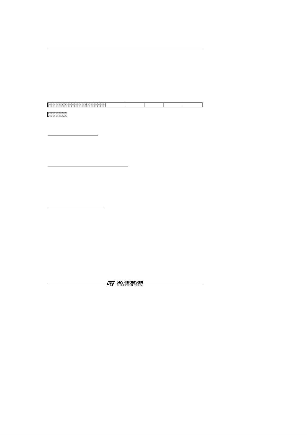
RegisterINDEX = C1h
76543210
NO-LOCK MMAC SMAC SMI RPL
Reserved
Table 2 - 1 CCR1 Register
ST486DX - SMMIMPLEMENTATION
15
The portions of the ConfigurationControl Registers(CCR1, CCR2, and CCR3)which applyto
SMM and power management are described in the following pages.
SMI Enable SMM Pins
SMI = 0: SMI# input pin is ignored and SMADS# output pin floats. Executionof
SGS Thomson specific SMM instructions willgenerate an invalidopcode exception.
SMI = 1: SMI# input/outputpin and SMADS# output pin are enabled.SMI must be set
to 1 before any attempted accessto SMMmemory is made.
SMAC SystemManagement Memory Access
SMAC = 0: All memoryaccesses in normal mode go to system memory with ADS# output
active. In normal mode, execution of SGS Thomson specific SMM instructions
generate an invalid opcode exception.
SMAC = 1: Memory accesseswhile in normal mode that fall within the specifiedSMM
address region generatean SMADS#output and access SMM memory. SMI#
input is ignored.
MMAC MainMemory Access
MMAC = 0: All Memory accesseswhile in SMM mode go to SMM memory with SMADS#
output active.
MMAC = 1: Data accesses while in SMM mode that fall within the specified SMM address
region will generate an ADS# output and access mainmemory. Code fetches
are not effected by the MMAC bit. Code fetches from the SMMaddress region
always generate an SMADS#output and access SMM memory. If both the
SMAC and MMAC bits are set to 1,the MMAC bit has precedence.

HALT Suspendon HALT.
HALT = 0: CPU does not entersuspend mode following execution of aHLT instruction
HALT = 1: CPU enters suspend mode following execution of a HLT instruction.
SUSP Enable Suspend Pins.
SUSP = 0: SUSP# input isignored and SUSPA#output floats.
SUSP = 1: SUSP# input and SUSPA# output are enabled.
Reg. INDEX = C2h
76543 2 1 0
SUSP BWRT BARB WT1 HALT LOCK-NW WBAK COP/Reserved
Table 2 - 2 CCR2
Reg. INDEX = C3h
76543 2 1 0
NMIEN SMI-LOCK
Reserved
Table 2 - 1 CCR3
ST486DX - SMMIMPLEMENTATION
16
SMI_LOCKSMM Register Lock.
SMI_LOCK = 0: Any program in normal mode,as well as SMM software, has access to all
ConfigurationControl Registers.
SMI_LOCK = 1: The following ConfigurationControl Register bits can not bemodified unless
operating inSMM mode:
SMI, SMAC, MMAC, NMIEN, SMI_LOCK, and SMAR registersize fields.
NMIEN NMIEnable.
NMIEN = 0: NMI (Non-MaskableInterrupt) is not recognized during SMM. One occurrence of
NMI is latched and serviced after SMM mode is exited. TheNMIEN bit should
be cleared before executing a RSM instruction to exitSMM.
NMIEN = 1: NMI is enabled during SMM. This bit should onlybe set temporarilywhile in the
SMM routine to allow NMI interrupts to be serviced. NMIENshould not be set
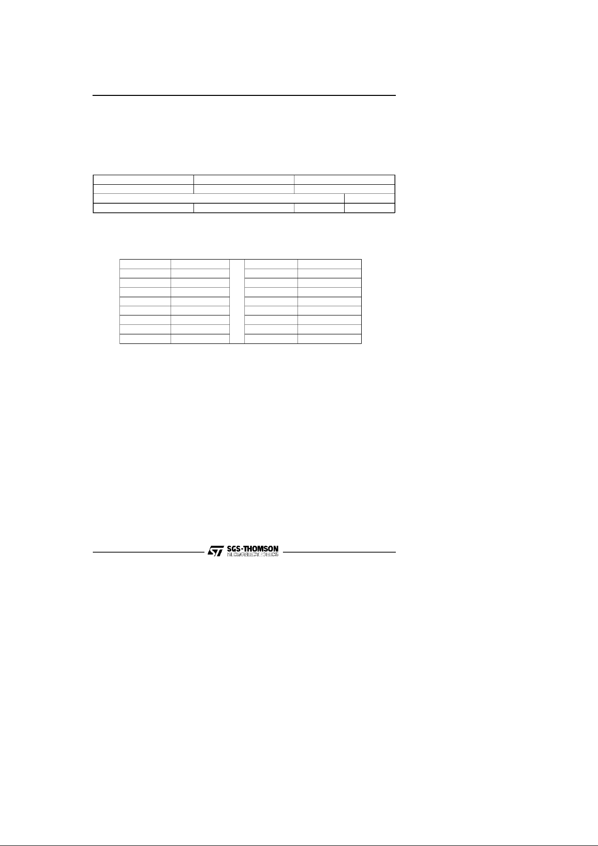
Reg. Index = CDh Reg.Index = CEh Reg. Index = CFh
70707430
BaseAddress Size
A31 A24 A23 A16 A15 A12 see table below
Table 2 - 3. SMAR SMM Address RegionRegisters
Bits 3-0 BLOCK SIZE Bits 3-0 BLOCK SIZE
0h Disable 8h 512 KBytes
1h 4 KBytes 9h 1MBytes
2h 8 KBytes Ah 2MBytes
3h 16 KBytes Bh 4 MBytes
4h 32 KBytes Ch 8 MBytes
5h 64 KBytes Dh 16MBytes
6h 128 KBytes Eh 32MBytes
7h 256 KBytes Fh 4 KBytes (same as 1h)
Table2 - 4. SMARSIZE FIELD
ST486DX - SMMIMPLEMENTATION
17
to 1 while in normal mode. If NMIEN = 1 when an SMI occurs, an NMI could
occur before the SMMcode has initialized the Interrupt Descriptor Table.
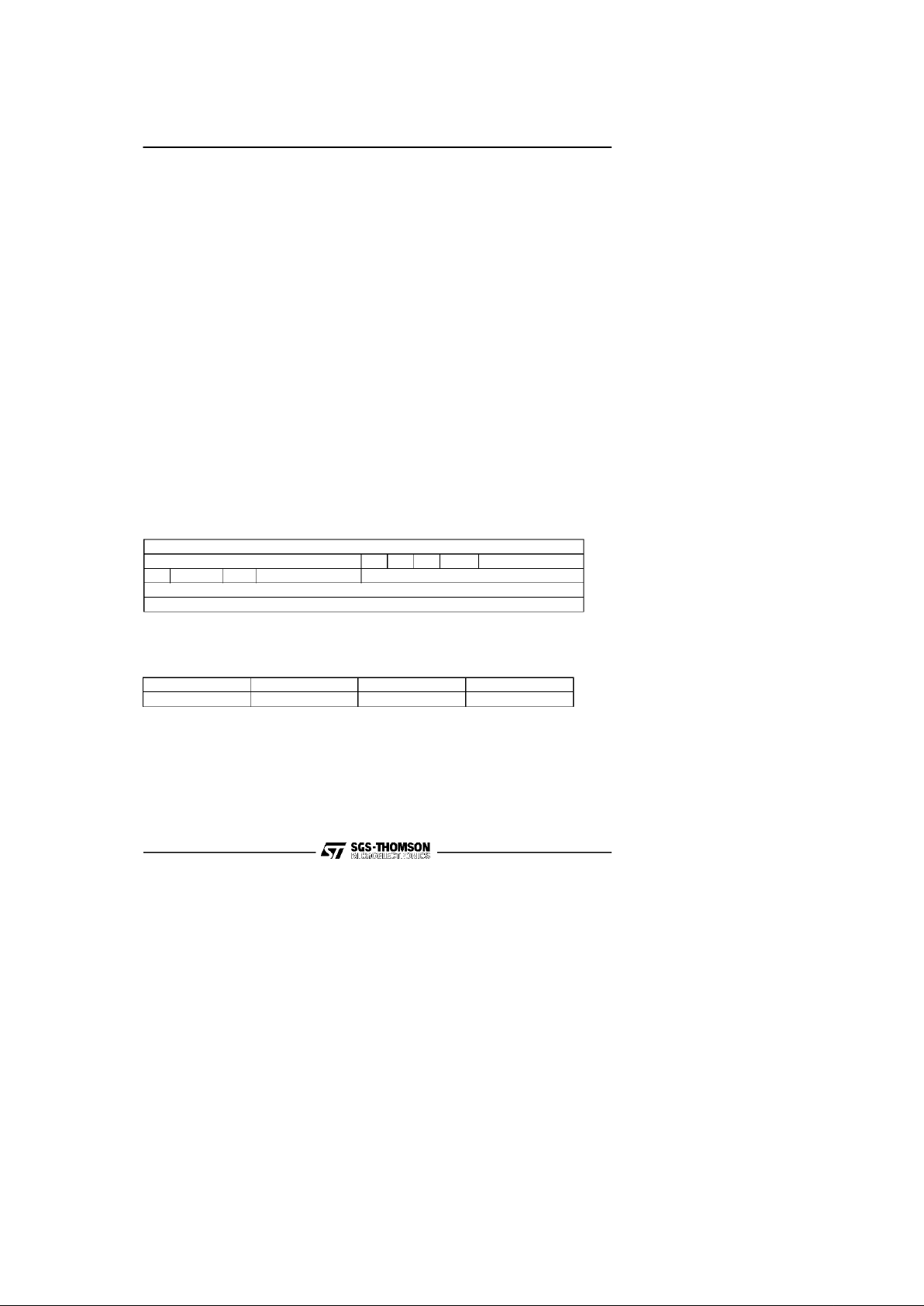
15 14 13 12 11 10 9 8 7 6 5 4 3 2 1 0
SELECTOR or SEGMENT +8
BASE 31 - 24 G D 0 AVL LIMIT 19 - 16 +6
P DPL DT TYPE BASE 23 - 16 +4
BASE 15 - 0 +2
LIMIT 15 - 0 +0
Table 2 - 5. Register and Descriptor Save Format
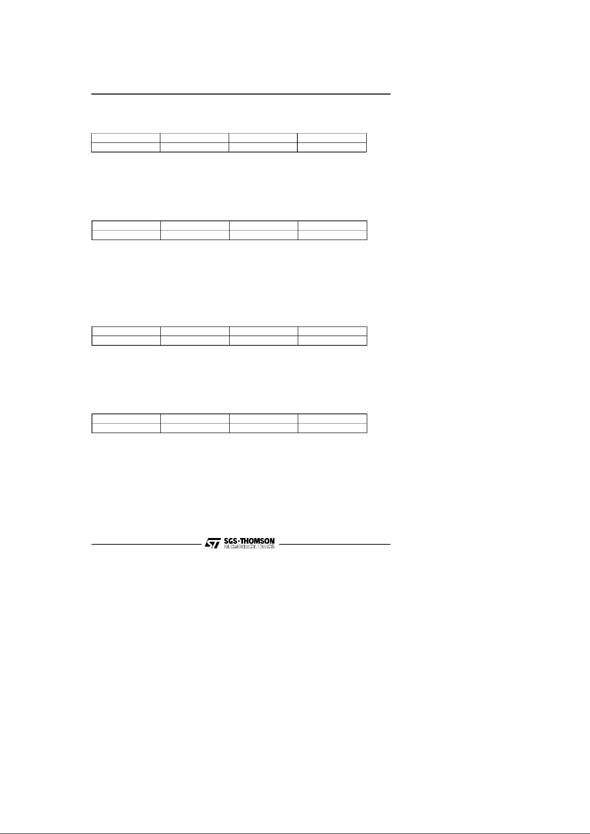
Instruction Opcode Parameters Core Clocks
RSDC 0F 79 [mod sreg3 r/m] sreg3,mem80 10
ST486DX - SMMIMPLEMENTATION
18
2.3 SMM Instruction Summary
SGS-Thomsonhas added seven new instructions to the X86 standard instruction set to aid in SMM
programming. These instructions are only valid when:
CPL = 0 and
SMI is enabled(CCR1 bit 1 = 1) and
SMAR size > 0 and
either [in SMM mode or SMAC is on (CCR1 bit 2 =1)]
The CPU will generate an undefined opcode fault when the aboveconditions are not met and one
of the SMM instructions are executed. The assembly languagemacro SMIMAC.INC listed in Appendix A will automatically generate the appropriate machine code when included in a source file
containing SGS-Thomson SMM instructions.
Most of the SGS-Thomson SMM instructions are used to access the non-programmer visibleinternal descriptors. Thestandard x86 instructionscan not access this information inside the CPU. This
information is stored in memory in a 10 Byte area that is comprised of both the descriptor (8-Bytes)
and the segment register/selector (2 Bytes). The 8 Byte descriptor is in the same format that is
found in the GDTor LDT. If the data area is dword aligned,it will minimize the memory access
time.
2.3.1 RSDC - RestoreRegister and Descriptor
RSDC loads the informationat the mem80 into a segment register/selector and its associated descriptor. Attemptingto use this instruction to load theCode Segment or CodeSelector will generate an invalid opcode instruction. Code Segment or Code Selector is restored from the SMM
header as part of the RSM instruction.
Instruction Opcode Parameters Core Clocks
RSM 0F AA None 76
Instruction Opcode Parameters Core Clocks
RSTS 0F 7D [mod 000 r/m] mem80 10
Instruction Opcode Parameters Core Clocks
SMINT 0F 7E None 24
Instruction Opcode Parameters Core Clocks
RSLDT 0F 7B[mod 000 r/m] mem80 10
2.3.2 RSLDT - Restore LDT and Descriptor
ST486DX - SMMIMPLEMENTATION
19
RSLDT loads the information at the mem80 into Local Descriptor Table Registerand its associated
descriptor.
2.3.3 RSM - Resume Back to Normal Mode
RSM will restore the state of the CPU from the SMM header at the top of SMM space and exit
SMM. This is the last instruction executed in an SMI handler. After theCPU state is restored,the
SMI#pin is driven inactivefor one clock then floated so the pin can be driven by the system.
2.3.4 RSTS - Restore TSR and Descriptor
RSTSloads the information at themem80 address into the Task Register and its associated
descriptor.
2.3.5 SMINT - SoftwareSMM Interrupt
SMINT will cause the CPU to enter SMM as though the hardwareSMI# pin was sampledlow.
The S bit in the SMMheader is set. The SMI# signal is not driven by the CPU when SMM is entered with SMINT.

Instruction Opcode Parameters Core Clocks
SVDC 0F 78 [mod sreg3 r/m] sreg3, mem80 18
Instruction Opcode Parameters Core Clocks
SVLDT 0F 7A [mod 000 r/m] mem80 18
Instruction Opcode Parameters Core Clocks
SVTS 0F 7C mem80 18
ST486DX - SMMIMPLEMENTATION
20
2.3.6 SVDC - SaveRegister and Descriptor
SVDC saves the contents of a segment register/selector and its associated descriptorto memory at
mem80. Thisinstruction can be used on any segment/selector includingthe CodeSegment.
2.3.7 SVLDT - SaveLDT and Descriptor
SVLDT savesthe Local Descriptor Table Selectorand non-programmervisible descriptor information at the address location mem80.
2.3.8 SVTS - Save TSR and Descriptor
SVTSsaves the Task Register and its associated descriptor to address location mem80.

ST486DX - SMMSOFTWARE CONSIDERATIONS
23
3. SMM SOFTWARE CONSIDERATIONS
This section provides an overview of SGS-Thomson SMM coding and information helpful in developing SMM code.
3.1 EnablingSMM
Many systems havememory controllers that aid in the initialization of SMM memory. SGS-Thomson SMM features allow the initialization of SMM memorywithout external hardware memory remapping.
When loading SMMmemory with an SMI interrupt handler it is important that the SMI# does not
occur before the handler is loaded. This can be done by notsetting SMAC=0 and SMI=1 before
the SMI handler is installed. It is necessary to load SMAR with appropriate values beforethe
SMM memory is accessible. Toload SMM memory with a program it is first necessary to enable
SMM memory withoutenabling the SMI pinsby setting SMAC. Setting SMI=1 will then map the
SMM memory region over mainmemory. TheSMM region isphysically mapped by the assertion
of SMADS# to allow memory access within the SMM region. A REP MOV instruction can then
be used to transfer the program to SMMmemory. After initializing SMM memory, negate SMAC
to activate potential SMI#s.
SMM space canbe locatedanywhere in the 4-GByte address range. However, if the location of
SMM space is beyond 1 Mbyte, the value in CS will truncatethe segmentabove 16-bits when
stored to the stack. Thiswould prohibit doing calls or interrupts from real mode without restoring
the 32-bit features of the 486 becauseof the incorrect return addresson the stack.
; load SMM memory from system memory
include SMIMAC.INC
SMMBASE = 68000h
SMMSIZE = 4000h ;SMM SIZE is 16K
SMI = 1 shl 1
SMAC = 1 shl 2
MMAC = 1 shl 3
mov al, 0cdh ;index SMAR, SMM baseA31-A24
out 22h, al ;select
mov al, 00h ;set high SMM address to 00
out 23h, al ;write value
mov al, 0ceh ;index SMAR,SMM baseA23-A16
out 22h, al ;select
mov al, 06h ;set mid SMM address to 06h
out 23h, al ;write value
mov al, 0cfh ;SMAR,SMM baseA15-A12 & SIZE

ST486DX - SMMSOFTWARE CONSIDERATIONS
24
out 22h, al ;select
mov al, 083h ;set SMM lower addr. 80h, 16K
out 23h, al ;write value
mov al, 0c1h ;index to CCR1
out 22h, al ;select CCR1 register
in al, 23h ;read current CCR1 value
mov ah, al ;save it
mov al, 0c1h ;index to CCR1
out 22h, al ;select CCR1 register
mov al, ah
or al, SMI or SMAC; set SMI and SMAC
out 23h, al ;new value now in CCR1, SMM now
;mapped in
mov ax, SMMBASE shr 4
mov es, ax
mov edi, 0 ;es:di = start of the SMM area
mov esi, offset SMI_ROUTINE ;start of copy of SMM
mov ax, seg SMI_ROUTINE ;routine in main memory
mov ds, ax
mov ecx, (SMI_ROUTINE_LENGTH+3)/4 ;calc. length
; this line copies the SMM routine from DS:ESI to ES:EDI
rep
movs dword ptr es:[edi],dword ptr ds:[esi]
; now disable SMI by clearing SMAC and SMI
mov al, 0c1h ;index to CCR1
out 22h, al ;select CCR1 register
mov al, ah ;AH is still old value
and al, NOT SMAC ;disable SMAC, enable SMI#
out 23h, al ;write new value to CCR
3.2 SMM Handler Entry State
At the beginning of the SMM routine, before control is transferred to code executing at the SMM
base, certain portions of the CPU state are saved at the top of SMM memory. To optimize the
speed of SMM entry and exit, the CPU saves the minimum CPU state information necessary for an
SMI interrupt handler to execute and return to the interruptedcontext. The information is saved to
the SMM header at the top of the defined SMM region(starting at SMM base + size - 30h) as
shown in Figure-3-1. Of the typically used program registers only the CS,IP, EFLAGS, CR0, and
DR7 are saved upon entry to SMM. This requiresthat data accesses use a CSsegment override to

DR7
EFLAGS
CR0
031
Top ofSMM
-4h
-8h
-Ch
-10h
-14h
-18h
-1Ch
-20h
-24h
-28h
P
Current IP
Next IP
Reserved
CS Selector
CS Descriptor (Bits 63-32)
CS Descriptor (Bits 31-0)
Reserved
ESI orEDI
I
1713503
31 16 15 0
31 2 1 0
-2Ch
-30h
Address Space
3
S
I/O Write AddressI/O Write Data Size
I/O Write Data
16 15
Figure 3 - 1. SMM Memory Space Header
ST486DX - SMMSOFTWARE CONSIDERATIONS
25
save other registersand access data in SMM memory. Touse any other register the SMM programmer must first save the contents using the SVDC instruction for segment registers or MOV operations for general purpose registers (SeeSGS Thomson SMM instruction description Section 2.3).
It is possible to saveall the CPU registers as needed. See Section 3.3 for an example saving and restoring the entire CPU state.

Bit Description Size
P REP INSx/OUTSx Indicator
0= Currentinstruction has a REP prefix
1= Currentinstruction does not have a REP prefix
1 bit
I IN, INSx, OUT, or OUTSx Indicator
0= Currentinstruction performed an I/O READ
1= Currentinstruction performed an I/O WRITE
1 bit
I/O Write Data Size Indicates size of data for the trappedI/O write
01h= byte
03h= word
0fh = dword
2 Bytes
I/O Write Address Address of the trappedI/O write 2 Bytes
I/O Write Date Data written during I/O trapped write 4 Bytes
ESI or EDI Value of appropriate index register before the trappedI/O instruction 4 Bytes
Table 3 - 1 I/O Trap Information
ST486DX - SMMSOFTWARE CONSIDERATIONS
26
Unique to the SGS-Thomson CPU is that theCPU saves the previous EIP (CURRENT_IP), before
the SMI event, and the next EIP (NEXT_IP) that will be executed after exiting theSMI handler.
Upon execution of an RSM instruction, control is returned to the NEXT_IP. The value of the
NEXT_IP may need to be modified for restarting I/O instructions. This modification is a simple
move (MOV) of the CURRENT_IP value to the NEXT_IP location. Execution is then returned to
the I/O instruction, rather than to the instructionafter the I/O instruction. Table 3-1 lists the SMM
header informationneeded to restart an I/O instruction. The restarting of I/O instructions may also
require modificationsto the ESI, ECX and EDIdepending on the instruction (see Section 3.6 for an
example.)
The EFLAGS, CR0 and DR7 registers are set to their reset values upon entry to the SMIhandler.
Resetting these registers has implications for setting breakpoints using the debug registers. Breakpoints can not be set prior to the SMI interruptusing debug registers. A debuggerwill only be able
to set a code breakpoint using INT 3 outside of the SMM handler. See Section 3.11 for restrictions
on debuggingSMM code. Once the SMI has occurred andthe debugger has control in SMM
space,the debug registerscan be usedfor the remainder of the SMI handler execution.
If the S bit in the SMM header is set, the SMM entry was the result of an SMINTinstruction.
Upon SMM entry, I/O trap informationis storedin the SMM memory space header. This informa-
tion allows restarting of I/O instructions, as well as the easy emulationof I/O functions by the
SMM handler. This data is only validif the instruction executing when the SMI occurred was an
I/O instruction. The three I/O Writefields (I/O Write Data, I/O Write Address and I/O Write Data
Size) are only valid when an I/O write was trapped.

Valid Cases P I
I/O Write
Data Size
I/O Write
Address
I/O Write
Data
ESI or
EDI
not an I/O ins. x x x x x x
IN 0 0 x x x EDI
INS 0 0 x x x EDI
REP INS 1 0 x x x EDI
OUT al 0 1 01h I/O Address xxxxxxdd ESI
OUT ax 0 1 03h I/O Address xxxxdddd ESI
OUT eax 0 1 0Fh I/O Address dddddddd ESI
OUTSB 0 1 01h I/O Address xxxxxxdd ESI
OUTSW 0 1 03h I/O Address xxxxdddd ESI
OUTSD 0 1 0Fh I/O Address dddddddd ESI
REP OUTSB 1 1 01h I/O Address xxxxxxdd ESI
REP OUTSW 1 1 03h I/O Address xxxxdddd ESI
REP OUTSD 1 1 0Fh I/O Address dddddddd ESI
Table 3 - 2 Valid I/O Trap Cases
x: invalid
CS SMM base specified by SMAR, CS limitis set to 4 GBytes
EIP 0000 0000h; Beginsexecutionat the base of SMM memory
EFLAGS 0000 0002h; Reset State
CR0 60000010h; Real Mode, Cache in Write Through
DR7 0000 0400h; Traps disabled
Table 3 - 3 SMM Entry State
ST486DX - SMMSOFTWARE CONSIDERATIONS
27
The values found in the I/O trap information fields are specifiedbelow for all cases.
Upon SMM entry, the CPU enters the following state:

ST486DX - SMMSOFTWARE CONSIDERATIONS
28
3.3 Maintainingthe CPU State
The following registers are not automatically saved/restored on SMM entry/exit.
General Purpose Registers: EAX, EBX, ECX, EDX
Pointer and Index Registers: EBP, ESI, EDI, ESP
Selector/Segment Registers: DS, ES, SS, FS, GS
Descriptor Table Registers: GDTR,IDTR, LDTR, TR
Control Registers: CR2, CR3
Debug Registers: DR0, DR1, DR2, DR3,DR6
ConfigurationRegisters: CCR1, CCR2, CCR3, SMAR
FPU Registers: Entire FPU state.
If any of these registers need to be usedby the SMM routine, theregisters need to be saved after entry to the SMM routine and then restoredprior to exit fromSMM. Additionally, if power is to be
removedfrom the CPU and the system is requiredto return to the same systemstate after power is
reapplied, then theentire CPU state mustbe saved to a non-volatilememory subsystemsuch as a
hard disk.
3.3.1 MaintainingCommon CPU Registers
The following is an example of the instructionsneeded to save the entire CPU state andrestore it.
This code sequence will work from real mode if the conditions needed to execute SGS-Thomson
SMM instructions are met(see Section 2.3).
; Save and Restore the common CPU registers.
; The information automatically saved in the
; header on entry to SMM is not saved again.
include SMIMAC.INC
.386P ;required for SMIMAC.INC macro
mov cs:save_eax,eax
mov cs:save_ebx,ebx
mov cs:save_ecx,ecx
mov cs:save_edx,edx
mov cs:save_esi,esi
mov cs:save_edi,edi
mov cs:save_ebp,ebp
mov cs:save_esp,esp
svdc cs:,save_ds,ds
svdc cs:,save_es,es
svdc cs:,save_fs,fs
svdc cs:,save_gs,gs
svdc cs:,save_ss,ss
svldt cs:,save_ldt ;sldt is not valid in real mode

ST486DX - SMMSOFTWARE CONSIDERATIONS
29
svts cs:,save_tsr ;str is not valid in real mode
db 66h ;32bit version saves everything
sgdt fword ptr cs:[save_gdt]
db 66h ;32bit version saves everything
sidt fword ptr cs:[save_idt]
; at the end of the SMM routine the following code
; sequence will reload the entire CPU state
mov eax,cs:save_eax
mov ebx,cs:save_ebx
mov ecx,cs:save_ecx
mov edx,cs:save_edx
mov esi,cs:save_esi
mov edi,cs:save_edi
mov ebp,cs:save_ebp
mov esp,cs:save_esp
rsdc ds,cs:,save_ds
rsdc es,cs:,save_es
rsdc fs,cs:,save_fs
rsdc gs,cs:,save_gs
rsdc ss,cs:,save_ss
rsldt cs:,save_ldt
rsts cs:,save_tsr
db 66h
sgdt fword ptr cs:[save_gdt]
db 66h
sidt fword ptr cs:[save_idt]
; the data space to save the CPU state is in
; the Code Segment for this example
save_ds dt ?
save_es dt ?
save_fs dt ?
save_gs dt ?
save_ss dt ?
save_ldt dt ?
save_tsr dt ?
save_eax dd ?
save_ebx dd ?
save_ecx dd ?
save_edx dd ?
save_esi dd ?
save_edi dd ?
save_ebp dd ?
save_esp dd ?
save_gdt df ?
save_idt df ?

ST486DX - SMMSOFTWARE CONSIDERATIONS
30
3.3.2 MaintainingControl Registers
CR0 is maintained in the SMM header. CR2 and CR3 need only be saved if the SMM routine will
be entering protected modeand enabling paging. MostSMM routines will not need to enablepaging. However, if the CPU is goingto be powered off, these registers like all the others need to be
saved.
3.3.3 MaintainingDebug Registers
DR7 is maintained in the SMM Header. Since DR7 is automatically initialized to the reset state on
entry to SMM, the Global Disable bit (DR7bit 13) will be cleared. This allows the SMM routine
to access all of the Debug Registers. Returning from the SMM handler will reload DR7 with its
previous value. In mostcases, SMM routines will not make use of the Debug Registers and they
will only need to be saved if the CPU needs to be powered down.
3.3.4 MaintainingConfiguration Control Registers
The SMM routine should be written so that it maintains the ConfigurationControl Registers in the
state that they were initialized to by the BIOS at power-up.
3.3.5 Maintaining FPU State
If power will be removed from the FPU, or if the SMM routine willexecute FPU instructions, then
the FPU state needs to be maintained for the application running before SMM was entered. If the
FPU state is to be saved and restored from within SMM, there are certain guidelinesthat must be
followed to make SMM completelytransparentto theapplication program.
The complete state of theFPU can be saved and restored with the FNSAVE and FNRSTORinstructions. FNSAVE is used instead of the FSAVE because FSAVE will wait for the FPUto check for
existing error conditions before storingthe FPU state. If there is a unmaskedFPU exception condition pending,the FSAVEinstruction will wait until the exception condition is serviced. In order to
be transparentto the application program, the SMM routine should not servicethe exception. If the
FPU state is restored with the FNRSTORinstruction before returning to normal mode, the application program can correctly service the exception. AnyFPU instructions can be executed within
SMM once the FPU state has been saved.
The information saved with the FSAVE instruction varies depending on the operatingmode of the
CPU. To save and restore allFPU information, the 32-bit protected mode version of the FPU save

ST486DX - SMMSOFTWARE CONSIDERATIONS
31
and restore instruction should be used. This can be accomplished by using the following code
example:
; Save the FPU state
mov eax,CR0
or eax,00000001h
mov CR0,eax ;set the PE bit in CR0
jmp $+2 ;clear the prefetch que
db 66h ;do 32bit version of fnsave
fnsave [save_fpu] ;saves fpu state to
;the address DS:[save_fpu]
mov eax,CR0
and eax, 0FFFFFFFEh ;clear PE bit in CR0
mov CR0,eax ;return to real mode
;now the SMM routine can do any FPU instruction.
;Restore the FPU state before executing a RSM
mov eax,CR0
or eax,00000001h
mov CR0,eax ;set the PE bit in CR0
jmp $+2 ;clear the prefetch que
db 66h ;do 32bit version of fnsave
frstor [save_fpu] ;restore the FPU state
;Some assemblers may require
;use of the fnrstor instruction
mov eax,CR0
and eax, 0FFFFFFFEh ;clear PE bit in CR0
mov CR0,eax ;return to real mode
Be surethat all interrupts are disabled before usingthis method for entering protected mode. Any
attempt to load a selector register while in protected mode will shutdown the CPU since no GDT is
set up. Settingup a GDT and doing a long jump to enter protected mode will also work correctly.
3.4 Initializing the SMM Environment
After enteringSMM and saving the CPU registers that will be usedby the SMM routine, afew
registersneed to be initialized.
Segment registers need to be initializedif the CPU was operating in protected modewhen the SMI
interrupt occurred. Segment registers that will be used by the SMM routine need to beloaded with
known limits before they are used. The protected mode application could have set a segment limit
to less than 64K. To avoid a protectionerror, all segment registers can be given limitsof 4 GBytes.
This can be done with the SGS Thomson RSDC instruction and will allow access to the

ST486DX - SMMSOFTWARE CONSIDERATIONS
32
full 4-GBytes of possible system memory without entering protected mode. Once the limits of a
segment register are set, the base can be changedby use of the MOV instruction.
An Interrupt Descriptor Table (IDT) needs to be set up in SMM memory before any interrupts or
exceptions occur. Once initialized, theSMI handler can execute calls, jumps, and other changes of
flow and will generatesoftware interrupts and faults. TheInterrupt Descriptor Table Register can
be loaded with an LIDT instruction to point to a small IDT in SMMmemory that can handle the
possibleinterrupts and exceptions that mightoccur while in the SMM routine.
A stack should always be set up in SMM memory so that stack operations done within SMM do not
affect the system memory.
; SMM environment initialization example
rsdc ds,cs:,seg4G ;DS is a 4GByte segment, base=0
rsdc es,cs:,seg4G ;ES is a 4GByte segment, base=0
rsdc fs,cs:,seg4G ;FS is a 4GByte segment, base=0
rsdc gs,cs:,seg4G ;GS is a 4GByte segment, base=0
rsdc ss,cs:,seg4G ;SS is a 4GByte segment, base=0
lidt cs:smm_idt ;load IDT base and limit for
;SMM’s IDT
mov esp, smm_stack
jmp continue_smm_code
;
;descriptor of 4GByte data segment for use by rsdc
seg4G dw 0ffffh ; limit 4G
dw 0 ; base = 0
db 0 ; base = 0
db 10010011B ; data segment, DPL=0,P=1
db 8fh ; limit = 4G,
db 0h ; base = 0
dw 0 ; segment register = 0
smm_idt dw smm_idt_limit
dd smm_idt_base
3.5 AccessingMain Memory Overlappedby SMM Memory
When in SMM mode there are instances where the programneeds access to the system memory
that is overlapping with SMM memory. Thisneed most commonly occurs when the SMMroutine
is trying to save the entire memory image to disk before powering down the system. To access
main memory overlapping the SMMspace (i.e., generate ADS# for memory MOV instructions
rather than SMADS#) set the MMAC bit in CCR1. The following codewill enable and then disable
MMAC:

ST486DX - SMMSOFTWARE CONSIDERATIONS
33
; Set MMAC to access main memory
MMAC = 1 shl 3
mov al, 0c1h ;select CCR1
out 22h, al
in al, 23h ;get CCR1 current value
mov ah, al ;save it
mov al, 0c1h ;select CCR1 again
out 22h, al
mov al, ah
or al, MMAC ;set MMAC
out 23h, al ;write new value to CCR1
;Now all data memory access will use ADS#, Code fetches
;will continue to be done with SMADS# from SMM memory.
;
;Disable MMAC
mov al, 0c1h ;select CCR1
out 22h, al
mov al, ah ;get old value of CCR1
out 23h, al ;and restore it
3.6 I/O Restart
When implementing power managementinto asystem it is common to want to power down peripheralswhen they are not in use. Whenan I/O instruction is issued to a powered down device, the
SMM routine is called to power up the peripheraland thenreissue the I/O instruction. SGS-Thomson CPUs make it easy to restart the I/O instruction that has generated an SMI interrupt.
The system will generate an SMI interruptwhen an I/O bus cycle to a powered-downperipheral is
detected. The SMM routine should interrogate the system hardware to find out if the SMI was
caused by an I/O trap. Bychecking the SMM header information, the SMM routine can determine
the type of I/O instruction thatwas trapped. If the I/O instruction has a REP prefix, the ECX register needs to be incremented before restarting the instruction. If the I/O trap was on a string I/O instruction,the ESI or EDI registersmust be restoredto their previous value before restarting the
instruction.
The following code example shows how easy I/O restart is with theSGS Thomson CPU.
;Restart the interrupted instruction
mov eax,dword ptr cs:[SMI_CURRENTIP]
mov dword ptr cs:[SMI_NEXTIP],eax
mov al,byte ptr cs:[SMI_BITS]
;test for REP instruction

ST486DX - SMMSOFTWARE CONSIDERATIONS
34
bt ax,2 ;rep instruction?
;(result to Carry)
adc ecx,0 ;if so, increment ecx
test al,1 shl 1 ;test bit 1 to see
;if an OUTS or INS
jnz out_instr
; A port read (INS or IN) instruction caused the
; chipset to generate an SMI instruction.
; Restore EDI from SMM header.
mov edi, dword ptr cs:[SMI_ESIEDI]
jmp common1
; A port write (OUTS or OUT) instruction caused the
; chipset to generate an SMI instruction.
; Restore ESI from SMM header.
out_instr:
mov esi, dword ptr cs:[SMI_ESIEDI]
common1:
3.7 I/O PortShadowingand Emulation
Some system peripherals contain write-only ports. In a system that does power management, these
peripherals need to be powered off and thenreinitialized when their functions are needed later. The
SGS Thomson SMM implementationmakes it very easy to monitor the last value written to specific I/O ports. This process is known as shadowing. If the system can generate anSMI whenever
specific I/O addressesget accessed, the SMM routine can, transparently to the system, monitor the
port activity. The SMMheader contains the address of the I/O write as wellas the data. In addition, information is savedwhich indicates whether it is a byte, word or dword write. With this information, shadowing systemwrite-only ports becomes trivial.
Some peripheral componentscontain registers that must be programmed in a specific order. If an
SMI interrupt occurs while an applicationis accessing this type of peripheral, the SMI routine must
be sure to reloadthe peripheral registers to the same stage before returning to normal mode. If the
SMM routine needs to access such a peripheral,the previous normal mode state must be restored.
The previousaccesses that were shadowed by previous SMM calls can be used to reload the peripheral registersback tothe stage wherethe application was interrupted. The application can then continue whereit left off accessing the peripheral.
In a similar way, the SGS-Thomson SMM implementation allows the SMM routine to emulatethe
function of peripheral components in software.

ST486DX - SMMSOFTWARE CONSIDERATIONS
35
3.8 Return to HLT Instruction
To make an SMI interrupt truly transparentto thesystem, an SMI interruptfrom a HLTinstruction
should return to the HLT instruction. There areknown cases with DOS software where returning
from an SMI handler to the instruction following the HLT will cause a system error. To determine
if a HLT instruction was interruptedby the SMI, the opcode from memory needs to be interrogated.
This code example describes how to determine if the current instructionis a HLT and howto
restart it.
;This is the start of specific code to check if the SMI
;occurred while in a HLT instruction. If it did, then
;return back to the HLT instruction when SMI is finished.
rsdc fs,cs:,[seg4G] ;FS is base=0 limit=4G data
;segment to be used to check if
;HLT instruction was executing
;on a SGS Thomson part, if the SMI occurred while in a HLT
;instruction, the CURRENT IP and the NEXT IP will both
;point to the instruction following the HLT.
mov eax,cs:dword ptr[SMI_CURRENTIP]
cmp eax,cs:dword ptr[SMI_NEXTIP]
jne not_hlt ;can’t be a HLT but could be
;a LOOP or REP
;load EAX with CS base from the SMM header
mov ax,cs:word ptr [SMI_CSSELH+2]
mov al,cs:byte ptr [SMI_CSSELH]
shl eax,10h
mov ax,cs:word ptr[SMI_CSSELL+2]
;calculate linear address
add eax,cs:dword ptr [SMI_CURRENTIP]
dec eax ;decrement to HLT instruction
mov edx,eax ;save lin addr in edx
mov eax,cs:dword ptr [SMI_CR0] ;check if paging on
test eax,80000000h
je no_paging ;if no paging then linear
;address = physical address
;set MMAC to get access to Main memory
mov al,0c1h
out 22h,al
in al,23h
mov cl,al ;save old CCR1 value in cl
mov al,0c1h
out 22h,al

ST486DX - SMMSOFTWARE CONSIDERATIONS
36
mov al,cl
or al,08h ;set MMAC bit in CCR1
mov al,0c1h
out 23h,al
mov eax,CR3 ;get Page Directory Base Reg
and eax,0fffff000h
mov ebx,edx ;linear address
shr ebx,22 ;get 10 byte Directory Entry
;read Directory Table
mov eax,dword ptr fs:[eax+ebx*4]
and eax,0fffff000h
mov ebx,edx ;linear address
shr ebx,12
and ebx,03ffh ;get 10 byte Page Table Entry
mov eax,dword ptr fs:[eax+ebx*4]
and eax,0fffff000h
mov ebx,edx ;linear address
and ebx,0fffh ;get 12 byte offset into page
;Get the physical address of the instruction before the
;Current IP. Save in BL.
mov bl,byte ptr fs:[eax+ebx]
mov al,0c1h ;set MMAC back to normal
out 22h,al
mov al,cl
out 23h,al ;MMAC = 0
jmp got_inst
;If paging is not enabled then checking for the HLT
;instruction is easy since the linear address equals
;the physical address.
no_paging:
mov al,0c1h ;set MMAC
out 22h,al
in al,23h
mov ah,al
mov al,0c1h
out 22h,al
mov al,ah
or al,08h
out 23h,al
;get instruction interrupted by SMI
mov bl,byte ptr fs:[edx]
mov al,0c1h ;store it in BL
out 22h,al

mov al,ah
out 23h,al ;set MMAC back to normal
got_inst:
cmp bl,0f4h ;was it a HLT instruction?
jne not_hlt ;if not a F4 then not a HLT
;set up SMM header to return
;to the HLT instruction
dec cs:dword ptr [SMI_NEXTIP]
not_hlt:
jmp continue_SMI_routine
; data within the SMM Space Code Segment
seg4G dw 0ffffh ;limit 15-0
dw 0 ;base
db 0 ;base
db 10010011B ;data segment, DPL=0, present
db 8Fh ;high limit =f, Gran =4K, 16 bit
db 0 ;base
dw 0
3.9 Exitingthe SMI Handler
When the RSM instruction is executed atthe end of the SMI handler,the EIP is loaded fromthe
SMM header at the address (SMMbase + SMMsize- 14h)called NEXT_IP. This permits the instruction to be restarted if NEXT_IP was modifiedby the SMM program. The valuesof ECX,ESI,
and EDI, prior to the executionof the instruction that was interrupted by SMI, can be restored from
information in theheader which pertains to the INxand OUTx instructions. See Section3.6 for an
exampleprogram to restartan I/O instruction. The only registersthat are restored fromthe SMM
header areCS, NEXT_IP, EFLAGS, CR0, and DR7. All other registerswhich were modified by
the SMM program need to be restored before executing the RSM instruction.
ST486DX - SMMSOFTWARE CONSIDERATIONS
37

3.10 Testingand Debugging SMM Code
An SMI routinecan be debugged with standard debugging tools (such as DOS DEBUG)if the
followingrequirements are met:
1. The debugger willonly be able to set a code break point using INT 3 outside of the SMI handler. The debug control register DR7 is setto the reset valueupon entry to the SMI handler.
Therefore, any break conditions in DR0-3 will be disabledafter entry to SMM. Debug registers can be used if set afterentry to the SMI handlerand DR0-3 aresaved.
2. The debugger needsto be running in real mode and the SMM routine can not enter protected
mode. This insures that normal system interrupts, BIOS calls and thedebugger will work
correctly from SMM mode.
3. Before an INT 3 break point is executed, all segment registers should have their limits modified to 64K, or larger, within the SMM routine.
ST486DX - SMMSOFTWARE CONSIDERATIONS
38

Option Typical CurrentOptions
Reduced Clock Frequency (13 x f
CLK
(MHz)) + 150 mA @ 5.0 V
5.0V operation 610 mA @ 33MHz, 765 mA @ 50 MHz
3.3V operation 360 mA @ 33MHz
RemoveClock 150 mA
SuspendMode clock operating 15 mA
SuspendMode and Remove Clock
450 µA
RemovePower 0 mA
Table 4 - 1 Power Management Options
Note: Values listed areapproximations. Refer to the appropriate SGS-Thomson data book for DC specifications.
ST486DX- SMM POWER MANAGEMENT FEATURES
41
4. Power Management Features
The SGS-Thomson CPU provides several methods and levels of power management. Thefully
static designallows clock stopping. Suspend Mode, SMM and 3.3 volt operation can be used to
achieve optimum CPU and system power management. Table 4-1 summarizes the various power
managementoptions for the SGS-Thomson CPU.
4.1 Reducing the Clock Frequency
The SGS-Thomson CPU is a fullystatic design meaning the input clock frequency can be reduced
or stoppedwithout a lossof internal CPU data or state. The system designer can makedecisions to
reduce the clock frequency by usingSGS-Thomson SMM capabilities, Advanced Power Management (APM) software API and/or chipset capabilities. When the clock is removed and then reasserted, execution will begin with the instruction where theclock was removed from the CPU.
4.2 Lowering the CPUSupply Voltage
SGS-Thomson CPUs are availablethat operate at either3.3 or 5.0 volts. Parts rated at 3.3volts
have the letter ’V’ included in the part number (Refer theappropriate SGS-Thomsondata book for
complete orderinginformation). The typical current (I
cc
) drawn by the SGS-Thomson CPU isreduced by approximately 50% when operating at 3.3 instead of 5.0 volts. Operating the CPU at3.3
volts can reduce CPU power consumption by over 70%, as the power consumptionincreasesas the
square of the power supply voltage (P-=-V
2
/R and P-=-CV2F).

ST486DX - SMMPOWER MANAGEMENT FEATURES
42
4.3 Suspend Mode
The SGS-Thomson CPU allows suspend mode to beentered either through software or hardware.
The software initiates suspend mode throughexecution of a HLT instruction if CCR2 bit 3 (HALT)
is set. After the HLT instruction is executed, the CPU enters suspend mode and asserts the suspend
acknowledge (SUSPA#) pin (if the SUSPbit in CCR2 was set to enable theSUSPA# pin).
Hardware initiatessuspend mode by using two new pins on the CPU,SUSP# and SUSPA#. When
SUSP# is asserted, the CPU first completesany pending instructions and bus cycles,and then enters
suspend mode. Once in suspend mode, the SUSPA# pin is asserted by the CPU.

ST486DX - ASSEMBLER MACROSFOR SGS-THOMSON INSTRUCTIONS
45
A. ASSEMBLER MACROS FOR SGS-THOMSON INSTRUCTIONS
The include file SMICAM.INCprovides a complex set of macros which generate SMM opcodes
along with the appropriate mod/rmbytes. Inorder to function, the macros require that the labels
whichare accessed correspond to the specified segment. Thus segment overrides must be passedto
the macro as an argument.
Do not specify a segment override if the default segment for an address is being used. If an address
size override is used, a final argument of ‘1’ mustbe passedto the macro as well. Address size
overrides must be presented explicitly to preventthe assembler from generating them automatically
and breaking the macros.
;SMM Instruction Macros - SMIMAC.INC
;Macros which generate mod/rm automatically
svdc MACRO segover,addr,reg,adover
domac segover,addr,reg,adover,78h
ENDM
rsdc MACRO reg,segover,addr,adover
domac segover,addr,reg,adover,79h
ENDM
svldt MACRO segover,addr,adover
domac segover,addr,es,adover,7ah
ENDM
rsldt MACRO segover,addr,adover
domac segover,addr,es,adover,7bh
ENDM
svts MACRO segover,addr,adover
domac segover,addr,es,adover,7ch
ENDM
rsts MACRO segover,addr,adover
domac segover,addr,es,adover,7dh
ENDM
rsm MACRO
db 0fh,0aah
ENDM
;Sub-Macro used by the above macro
domac MACRO segover,addr,reg,adover,op
local place1,place2,count
count = 0
ifnb < adover >
count=count+1
endif
ifnb < segover >

ST486DX - ASSEMBLER MACROS FOR SGS-THOMSON INSTRUCTIONS
46
count=count+1
endif
if (count eq 0)
nop ;expanding the opcode one byte
endif
place1 = $
;pull off the proper prefix byte count
mov word ptr segover addr,reg
org place1+count
mov word ptr segover addr,reg
place2 = $
;patch the opcode
org place1+(count*2)-1
db 0Fh,op
org place2
ENDM
;Offset Definition for access into SMM space
SMI_SAVE STRUC
$ESIEDI DD ?
$IOWDATA DD ?
$IOWADDR DW ?
$IOWSIZE DW ?
$BITS DD ?
$CSSELL DD ?
$CSSELH DD ?
$CS DW ?
$RES1 DW ?
$NEXTIP DD ?
$CURRENTIP DD ?
$CR0 DD ?
$EFLAGS DD ?
$DR7 DD ?
SMI_SAVE ENDS
SMI_ESIEDI EQU ($ESIEDI + SMMSIZE - SIZE SMI_SAVE)
SMI_IOWDATA EQU ($IOWDATA+ SMMSIZE - SIZE SMI_SAVE)
SMI_IOWADDR EQU ($IOWADDR+ SMMSIZE - SIZE SMI_SAVE)
SMI_IOWSIZE EQU ($IOWSIZE+ SMMSIZE - SIZE SMI_SAVE)
SMI_BITS EQU ($BITS + SMMSIZE - SIZE SMI_SAVE)
SMI_CSSELL EQU ($CSSELL + SMMSIZE - SIZE SMI_SAVE)
SMI_CSSELH EQU ($CSSELH + SMMSIZE - SIZE SMI_SAVE)
SMI_CS EQU ($CS + SMMSIZE - SIZE SMI_SAVE)
SMI_RES1 EQU ($RES1 + SMMSIZE - SIZE SMI_SAVE)
SMI_NEXTIP EQU ($NEXTIP + SMMSIZE - SIZE SMI_SAVE)
SMI_CURRENTIP EQU ($CURRENTIP+ SMMSIZE -SIZE SMI_SAVE)

ST486DX - ASSEMBLER MACROSFOR SGS-THOMSON INSTRUCTIONS
47
SMI_CR0 EQU ($CR0 + SMMSIZE - SIZE SMI_SAVE)
SMI_EFLAGS EQU ($EFLAGS + SMMSIZE - SIZE SMI_SAVE)
SMI_DR7 EQU ($DR7 + SMMSIZE - SIZE SMI_SAVE)
SMM Instruction macro example: TEST.ASM
.MODEL SMALL
.386
;SMM Macro Examples
; by Dean C. Wills
include smimac.inc
0000 .DATA
0000 0A*(??) there db 10 dup (?)
000A .CODE
0000 2E 0F 78 1E 004E svdc cs:,hello,ds
0006 2E 0F 79 1E 004E rsdc ds,cs:,hello
000C 2E 0F 79 2E 004E rsdc gs,cs:,hello
0012 2E 67 2E 0F 78 9C 58 0000004E
svdc cs:,[eax+ebx*2+hello],1
001D 67| 0F 78 23 svdc ,[ebx],fs,1
0021 0F 78 2E 0000 svdc ,there,gs
0026 2E 0F 7A 06 004E svldt cs:,hello
002C 2E 0F 7B 06 004E rsldt cs:,hello
0032 2E 0F 7D 06 004E rsts cs:,hello
0038 2E 67 2E 0F 7C 84 58 0000004E
svts cs:,[eax+ebx*2+hello],1
0043 67| 0F 7A 03 svldt ,[ebx],1
0047 0F 7C 06 0000 svts ,there
004C 0F AA rsm
004E 0A*(??) hello db 10 dup (?)
end

Information furnished is believed to be accurate and reliable. However, SGS-THOMSON Microelectronics assumes no responsibility for the
consequences of use of such information nor for any infringement of patents or other rights of third parties which may result from its use. No
licenseis granted by implicationor otherwise under any patent or patentrights of SGS-THOMSON Microelectronics.Specificationmentioned in
thispublication are subject tochange withoutnotice.This publication supersedes and replacesall information previouslysupplied. SGS-THOMSON
Microelectronicsproducts are notauthorized for use as critical componentsin life support devices or systems without express written approval of
SGS-THOMSON Microelectronics.
1995 SGS-THOMSON Microelectronics – Printed in Italy– All Rights Reserved
SGS-THOMSONMicroelectronics GROUP OF COMPANIES
Australia- Brazil - China - France - Germany - Hong Kong - Italy - Japan- Korea - Malaysia - Malta - Morocco - The Netherlands -
Singapore - Spain - Sweden - Switzerland - Taiwan - Thailand- United Kingdom - U.S.A.
 Loading...