

DATASHEET
13 August 2003 ADCS 7260755H STMicroelectronics 1/94
Overview
The ST40RA is the first member of the ST40 family. Based
on the SH-4, SuperH CPU core from SuperH Inc, the
ST40RA is designed to work as a standalone device, or as
part of a two chip solution for application specific systems.
Example applications the ST40RA is designed for include
digital consumer, embedded communications, industrial
and automotive. The high connectivity of the ST40 through
its PCI bus and its dual memory uses makes it a versatile
device, ideal for data-intensive and high performance
applications.
System features
■ 32-bit SuperH CPU
● 64-bit hardware FPU (1. 1 6 G F L O P S )
● 128-bit vector unit for matrix manipulations
● 166 MHz, 300 MIPS (DMIPS 1.1)
● Up to 664 Mbytes/s CPU bandwidth
● Direct mapped, on-chip, ICache (8 Kbytes) and DCache
(16 Kbytes)
■ High-performance 5-channel DMA engine,
supporting 1D or 2D block moves and linked lists
■ SuperHyway internal interco nne ct
● High throughput , low latency, split transact ion packet
router
■ Memory protection and VM system support
● 64-entry unified TLB, 4-entry instruction TLB
● 4 Gbytes address space
■ Standard ST40 peripherals
● 2 synchronous serial ports with FIFO (SCIF)
● Ti me rs and a real-time clock
IO devices
● Mailbox register for interprocessor comm unication
● Additional PIO
Bus interfaces
■ Local memory interface SDRAM & DDR SDRAM
● Up to 100 MHz (1.6 Gbytes/s peak throughput)
■ PCI interface - 32-bit, 66/33 MHz, 3.3 V
■ Enhanced memory interface (EMI)
● 32-bit bus, up to 83 MHz, for attaching peripherals
● High-speed, sync mode, burst flash ROM support
● SDRAM support
● MPX initiator and t arget interface
● Programmable MPX bus arbiter
Integer & FP
execution units
Registers
Interrupt ctrl
Real-time clock
Timer (TMU)
SCIF
Clock ctrl
SCIF
5 channel
controller
ST40 Local Memory I/F
32 data 64 data
32 data
2 channel
control
PIO
interface
JTAG
UDI
EMI
SuperHyway
PCI I/F 66MHz
Debug
PLLs
MMU
I Cache
MMU
D Cache
Cbus Bridge/
SuperHyway I/F
24 data
JTAG
DMA
PCI Peripherals SDRAM
MPX
Flash
Peripherals
Coprocessor
Mailbox
ST40RA
32-bit Embedded SuperH Device

ADCS 7260755H STMicroelectronics 2/94
ST40RA
Table of Contents
Chapter 1 Scope of this document . . . . . . . . . . . . . . . . . . . . . . . . . . . . . . . . . . . . . . . . . . . . .6
Chapter 2 ST40 documentation suite . . . . . . . . . . . . . . . . . . . . . . . . . . . . . . . . . . . . . . . . . . .6
CPU documentation . . . . . . . . . . . . . . . . . . . . . . . . . . . . . . . . . . . . . . . . . . . . . . . . . . . . . . 6
System documentation . . . . . . . . . . . . . . . . . . . . . . . . . . . . . . . . . . . . . . . . . . . . . . . . . . . . 6
Chapter 3 ST40RA devices . . . . . . . . . . . . . . . . . . . . . . . . . . . . . . . . . . . . . . . . . . . . . . . . . .6
Chapter 4 Architecture . . . . . . . . . . . . . . . . . . . . . . . . . . . . . . . . . . . . . . . . . . . . . . . . . . . . . .7
4.1 Overview . . . . . . . . . . . . . . . . . . . . . . . . . . . . . . . . . . . . . . . . . . . . . . . . . . . . . . . . . . . . . . . 7
4.2 ST40 system . . . . . . . . . . . . . . . . . . . . . . . . . . . . . . . . . . . . . . . . . . . . . . . . . . . . . . . . . . . . 7
4.2.1 SuperH ST40 SH-4 core . . . . . . . . . . . . . . . . . . . . . . . . . . . . . . . . . . . . . . . . . . . . . . . . . . . . . . . . . . 7
4.2.2 SuperHyway internal interconnect . . . . . . . . . . . . . . . . . . . . . . . . . . . . . . . . . . . . . . . . . . . . . . . . . . . 8
4.2.3 Standard ST40 peripherals . . . . . . . . . . . . . . . . . . . . . . . . . . . . . . . . . . . . . . . . . . . . . . . . . . . . . . . . 8
4.3 Bus interfaces . . . . . . . . . . . . . . . . . . . . . . . . . . . . . . . . . . . . . . . . . . . . . . . . . . . . . . . . . . . 9
4.3.1 Local memory interface . . . . . . . . . . . . . . . . . . . . . . . . . . . . . . . . . . . . . . . . . . . . . . . . . . . . . . . . . . . 9
4.3.2 PCI interface . . . . . . . . . . . . . . . . . . . . . . . . . . . . . . . . . . . . . . . . . . . . . . . . . . . . . . . . . . . . . . . . . . 10
4.3.3 EMI/MPX interface . . . . . . . . . . . . . . . . . . . . . . . . . . . . . . . . . . . . . . . . . . . . . . . . . . . . . . . . . . . . . 10
4.4 I/O devices . . . . . . . . . . . . . . . . . . . . . . . . . . . . . . . . . . . . . . . . . . . . . . . . . . . . . . . . . . . . 10
4.4.1 Mailbox . . . . . . . . . . . . . . . . . . . . . . . . . . . . . . . . . . . . . . . . . . . . . . . . . . . . . . . . . . . . . . . . . . . . . . 10
4.5 Software . . . . . . . . . . . . . . . . . . . . . . . . . . . . . . . . . . . . . . . . . . . . . . . . . . . . . . . . . . . . . . 10
4.5.1 Development systems and software . . . . . . . . . . . . . . . . . . . . . . . . . . . . . . . . . . . . . . . . . . . . . . . . 10
4.5.2 Software compatibility . . . . . . . . . . . . . . . . . . . . . . . . . . . . . . . . . . . . . . . . . . . . . . . . . . . . . . . . . . . 11
Chapter 5 System configuration . . . . . . . . . . . . . . . . . . . . . . . . . . . . . . . . . . . . . . . . . . . . . .11
5.1 System addresses . . . . . . . . . . . . . . . . . . . . . . . . . . . . . . . . . . . . . . . . . . . . . . . . . . . . . . . 12
5.1.1 System address map . . . . . . . . . . . . . . . . . . . . . . . . . . . . . . . . . . . . . . . . . . . . . . . . . . . . . . . . . . . . 1 3
5.2 System identifiers . . . . . . . . . . . . . . . . . . . . . . . . . . . . . . . . . . . . . . . . . . . . . . . . . . . . . . . 14
5.3 Interrupt mapping . . . . . . . . . . . . . . . . . . . . . . . . . . . . . . . . . . . . . . . . . . . . . . . . . . . . . . . 15
5.3.1 ST40 core interrupt allocation . . . . . . . . . . . . . . . . . . . . . . . . . . . . . . . . . . . . . . . . . . . . . . . . . . . . . 15
5.3.2 ST40 standard system interrupt allocation . . . . . . . . . . . . . . . . . . . . . . . . . . . . . . . . . . . . . . . . . . . 16
5.3.3 ST40RA I/O device interrupt allocation . . . . . . . . . . . . . . . . . . . . . . . . . . . . . . . . . . . . . . . . . . . . . . 17
5.4 GPDMA channel mapping . . . . . . . . . . . . . . . . . . . . . . . . . . . . . . . . . . . . . . . . . . . . . . . . . 17
5.5 EMI DACK mapping . . . . . . . . . . . . . . . . . . . . . . . . . . . . . . . . . . . . . . . . . . . . . . . . . . . . . 18
5.6 EMI address pin mapping . . . . . . . . . . . . . . . . . . . . . . . . . . . . . . . . . . . . . . . . . . . . . . . . . 18

ST40RA
3/94 STMicroelectronics ADCS 7260755H
5.7 EMI pin to function relationship . . . . . . . . . . . . . . . . . . . . . . . . . . . . . . . . . . . . . . . . . . . . . 19
5.8 Memory bridge control . . . . . . . . . . . . . . . . . . . . . . . . . . . . . . . . . . . . . . . . . . . . . . . . . . . 21
5.8.1 Memory bridge control signals . . . . . . . . . . . . . . . . . . . . . . . . . . . . . . . . . . . . . . . . . . . . . . . . . . . . 22
5.8.2 Memo ry bridge status . . . . . . . . . . . . . . . . . . . . . . . . . . . . . . . . . . . . . . . . . . . . . . . . . . . . . . . . . . . 22
5.8.3 Changing control of a memory bridge . . . . . . . . . . . . . . . . . . . . . . . . . . . . . . . . . . . . . . . . . . . . . . . 22
5.9 System configuration registers . . . . . . . . . . . . . . . . . . . . . . . . . . . . . . . . . . . . . . . . . . . . . 23
5.9.1 EMI.GENCFG EMI general configuration . . . . . . . . . . . . . . . . . . . . . . . . . . . . . . . . . . . . . . . . . . . . 24
5.9.2 LMI.COC . . . . . . . . . . . . . . . . . . . . . . . . . . . . . . . . . . . . . . . . . . . . . . . . . . . . . . . . . . . . . . . . . . . . . 2 5
5.9.3 LMI.CIC . . . . . . . . . . . . . . . . . . . . . . . . . . . . . . . . . . . . . . . . . . . . . . . . . . . . . . . . . . . . . . . . . . . . . . 26
5.9.4 SYSCO NF registers . . . . . . . . . . . . . . . . . . . . . . . . . . . . . . . . . . . . . . . . . . . . . . . . . . . . . . . . . . . . 26
5.9.5 SYSCONF.SYS_CON2. . . . . . . . . . . . . . . . . . . . . . . . . . . . . . . . . . . . . . . . . . . . . . . . . . . . . . . . . . 27
5.9.6 PIO alternate fu nctions . . . . . . . . . . . . . . . . . . . . . . . . . . . . . . . . . . . . . . . . . . . . . . . . . . . . . . . . . . 2 9
5.9.7 PCI.PERF register definition. . . . . . . . . . . . . . . . . . . . . . . . . . . . . . . . . . . . . . . . . . . . . . . . . . . . . . 30
Chapter 6 Clock generation . . . . . . . . . . . . . . . . . . . . . . . . . . . . . . . . . . . . . . . . . . . . . . . . .30
6.1 Clock domains and sources . . . . . . . . . . . . . . . . . . . . . . . . . . . . . . . . . . . . . . . . . . . . . . . 30
6.2 Recommended operating modes . . . . . . . . . . . . . . . . . . . . . . . . . . . . . . . . . . . . . . . . . . . 34
6.3 Clocks and registers at start up . . . . . . . . . . . . . . . . . . . . . . . . . . . . . . . . . . . . . . . . . . . . . 34
6.3.1 CLOCKGENA_2x PCI (PCI_DIV_BYPASS = 0) . . . . . . . . . . . . . . . . . . . . . . . . . . . . . . . . . . . . . . . 3 5
6.3.2 Division ratios on CLOCKGENA_2x. . . . . . . . . . . . . . . . . . . . . . . . . . . . . . . . . . . . . . . . . . . . . . . . . 35
6.4 Setting clock frequencies . . . . . . . . . . . . . . . . . . . . . . . . . . . . . . . . . . . . . . . . . . . . . . . . . 36
6.4.1 Programming the PLL output frequency . . . . . . . . . . . . . . . . . . . . . . . . . . . . . . . . . . . . . . . . . . . . . 37
6.4.2 Changing clock frequency . . . . . . . . . . . . . . . . . . . . . . . . . . . . . . . . . . . . . . . . . . . . . . . . . . . . . . . . 37
6.4.3 Changing the core PLL frequencies . . . . . . . . . . . . . . . . . . . . . . . . . . . . . . . . . . . . . . . . . . . . . . . . 37
6.4.4 Changing the frequency division ratio . . . . . . . . . . . . . . . . . . . . . . . . . . . . . . . . . . . . . . . . . . . . . . . 38
6.5 Power management . . . . . . . . . . . . . . . . . . . . . . . . . . . . . . . . . . . . . . . . . . . . . . . . . . . . . 38
6.5.1 CPU low-power modes . . . . . . . . . . . . . . . . . . . . . . . . . . . . . . . . . . . . . . . . . . . . . . . . . . . . . . . . . . 38
6.5.2 Module low-power modes . . . . . . . . . . . . . . . . . . . . . . . . . . . . . . . . . . . . . . . . . . . . . . . . . . . . . . . . 38
6.6 Clock generation registers . . . . . . . . . . . . . . . . . . . . . . . . . . . . . . . . . . . . . . . . . . . . . . . . 38
6.6.1 CLOCKGENB.CLK_SELCR register . . . . . . . . . . . . . . . . . . . . . . . . . . . . . . . . . . . . . . . . . . . . . . . 39
6.6.2 CPG.STBCR register . . . . . . . . . . . . . . . . . . . . . . . . . . . . . . . . . . . . . . . . . . . . . . . . . . . . . . . . . . 40
6.6.3 CLOCKGENA.STBREQCR and CLOC KGEN B.STBRE QCR registers . . . . . . . . . . . . . . . . . . . . . . 41
6.6.4 CLOCKGENA.STBREQCR_SET and CLOCKGENB.STBREQCR_SET registers . . . . . . . . . . . . . 41
6.6.5 CLOCKGENA.STBREQCR_CLR and CLOCKGENB.STBREQCR_CLR register . . . . . . . . . . . . 4 1
6.6.6 CLOCKGENA.STBACKCR and CLOCKGENB.STBACKCR register . . . . . . . . . . . . . . . . . . . . . . 42
Chapter 7 Electrical specifications . . . . . . . . . . . . . . . . . . . . . . . . . . . . . . . . . . . . . . . . . . .43
7.1 DC absolute maximum ratings . . . . . . . . . . . . . . . . . . . . . . . . . . . . . . . . . . . . . . . . . . . . . 43

ADCS 7260755H STMicroelectronics 4/94
ST40RA
7.1.1 Fmax clock domains . . . . . . . . . . . . . . . . . . . . . . . . . . . . . . . . . . . . . . . . . . . . . . . . . . . . . . . . . . . 43
7.1.2 Ope rating conditions . . . . . . . . . . . . . . . . . . . . . . . . . . . . . . . . . . . . . . . . . . . . . . . . . . . . . . . . . . . 44
7.1.3 Pad specific output AC characteristics . . . . . . . . . . . . . . . . . . . . . . . . . . . . . . . . . . . . . . . . . . . . . 45
7.2 Rise and fall times . . . . . . . . . . . . . . . . . . . . . . . . . . . . . . . . . . . . . . . . . . . . . . . . . . . . . 47
7.3 PCI interface AC specifications . . . . . . . . . . . . . . . . . . . . . . . . . . . . . . . . . . . . . . . . . . . 50
7.4 LMI interface (SDRA M) AC specifications . . . . . . . . . . . . . . . . . . . . . . . . . . . . . . . . . . . 51
7.5 LMI interface (DDR-SDRAM) AC specifications . . . . . . . . . . . . . . . . . . . . . . . . . . . . . . . 52
7.6 DDR bus termination (SSTL_2) . . . . . . . . . . . . . . . . . . . . . . . . . . . . . . . . . . . . . . . . . . . . 53
7.7 General purpose periph eral bus (EMI ) AC specific at ions . . . . . . . . . . . . . . . . . . . . . . . 54
7.8 PIO AC specifications . . . . . . . . . . . . . . . . . . . . . . . . . . . . . . . . . . . . . . . . . . . . . . . . . . . . 55
7.9 System CLKIN AC specifications . . . . . . . . . . . . . . . . . . . . . . . . . . . . . . . . . . . . . . . . . . . 56
7.10 Low power CLKIN AC specifications . . . . . . . . . . . . . . . . . . . . . . . . . . . . . . . . . . . . . . . . . 57
7.11 UDI and IEEE 1149.1 TAP AC specifications . . . . . . . . . . . . . . . . . . . . . . . . . . . . . . 58
Chapter 8 Pin description . . . . . . . . . . . . . . . . . . . . . . . . . . . . . . . . . . . . . . . . . . . . . . . . . . .59
8.1 Function pin use selection . . . . . . . . . . . . . . . . . . . . . . . . . . . . . . . . . . . . . . . . . . . . . . . . . 59
8.2 Mode selection . . . . . . . . . . . . . . . . . . . . . . . . . . . . . . . . . . . . . . . . . . . . . . . . . . . . . . . . . 59
8.3 PBGA 27 x 27 ba llout . . . . . . . . . . . . . . . . . . . . . . . . . . . . . . . . . . . . . . . . . . . . . . . . . . . . 61
8.4 Pin states . . . . . . . . . . . . . . . . . . . . . . . . . . . . . . . . . . . . . . . . . . . . . . . . . . . . . . . . . . . . . 72
Chapter 9 Package . . . . . . . . . . . . . . . . . . . . . . . . . . . . . . . . . . . . . . . . . . . . . . . . . . . . . . . . .75
Appendix A Interconnect architecture. . . . . . . . . . . . . . . . . . . . . . . . . . . . . . . . . . . . . . . . . . .78
A.1 Arbitration scheme s . . . . . . . . . . . . . . . . . . . . . . . . . . . . . . . . . . . . . . . . . . . . . . . . . . . . . . 79
A.1.1 PCI arbiter: (CPU, GPDMA, PCI, EMPI) . . . . . . . . . . . . . . . . . . . . . . . . . . . . . . . . . . . . . . . . . . . . 79
A.1.2 EMI arbiter: (CPU buffer, GPDMA, PCI, EMPI) . . . . . . . . . . . . . . . . . . . . . . . . . . . . . . . . . . . . . . . . 79
A.1.3 LMI 1 arbiter: (CPU, GPDMA, PCI, EMPI). . . . . . . . . . . . . . . . . . . . . . . . . . . . . . . . . . . . . . . . . . . . 79
A.1.4 PER arbiter: (CPU, GPDMA, PCI, EMPI). . . . . . . . . . . . . . . . . . . . . . . . . . . . . . . . . . . . . . . . . . . . . 79
A.1.5 LMI2 arbiter: (CPU, GPDMA, PCI, EMPI) . . . . . . . . . . . . . . . . . . . . . . . . . . . . . . . . . . . . . . . . . . . . 80
A.1.6 Return arbitration . . . . . . . . . . . . . . . . . . . . . . . . . . . . . . . . . . . . . . . . . . . . . . . . . . . . . . . . . . . . . . . 80
A.2 Interconnect registers. . . . . . . . . . . . . . . . . . . . . . . . . . . . . . . . . . . . . . . . . . . . . . . . . . . . . 80
A.2.1 LMI1 arbiter . . . . . . . . . . . . . . . . . . . . . . . . . . . . . . . . . . . . . . . . . . . . . . . . . . . . . . . . . . . . . . . . . . . 81
A.2.2 LMI2 arbiter . . . . . . . . . . . . . . . . . . . . . . . . . . . . . . . . . . . . . . . . . . . . . . . . . . . . . . . . . . . . . . . . 82
A.2.3 EMI arbiter . . . . . . . . . . . . . . . . . . . . . . . . . . . . . . . . . . . . . . . . . . . . . . . . . . . . . . . . . . . . . . . . . . . 83
A.2.4 PCI arbiter . . . . . . . . . . . . . . . . . . . . . . . . . . . . . . . . . . . . . . . . . . . . . . . . . . . . . . . . . . . . . . . . . . 84
A.2.5 Peripheral arbiter . . . . . . . . . . . . . . . . . . . . . . . . . . . . . . . . . . . . . . . . . . . . . . . . . . . . . . . . . . . . . 85
Appendix B Implementation restrictions . . . . . . . . . . . . . . . . . . . . . . . . . . . . . . . . . . . . . . . . .87

ST40RA
5/94 STMicroelectronics ADCS 7260755H
B.1 ST40 CPU . . . . . . . . . . . . . . . . . . . . . . . . . . . . . . . . . . . . . . . . . . . . . . . . . . . . . . . . . . . . . 87
B.1.1 tas.b . . . . . . . . . . . . . . . . . . . . . . . . . . . . . . . . . . . . . . . . . . . . . . . . . . . . . . . . . . . . . . . . . . . . . . . . . 87
B.1.2 Store que ue power-down. . . . . . . . . . . . . . . . . . . . . . . . . . . . . . . . . . . . . . . . . . . . . . . . . . . . . . . . . 8 7
B.1.3 UBC power-down . . . . . . . . . . . . . . . . . . . . . . . . . . . . . . . . . . . . . . . . . . . . . . . . . . . . . . . . . . . . . . . 87
B.1.4 Sy stem standby . . . . . . . . . . . . . . . . . . . . . . . . . . . . . . . . . . . . . . . . . . . . . . . . . . . . . . . . . . . . . . . . 87
B.2 PCI. . . . . . . . . . . . . . . . . . . . . . . . . . . . . . . . . . . . . . . . . . . . . . . . . . . . . . . . . . . . . . . . . . . 87
B.2.1 Clocking . . . . . . . . . . . . . . . . . . . . . . . . . . . . . . . . . . . . . . . . . . . . . . . . . . . . . . . . . . . . . . . . . . . . . . 87
B.2.2 Type 2 configuration accesses. . . . . . . . . . . . . . . . . . . . . . . . . . . . . . . . . . . . . . . . . . . . . . . . . . . . . 8 7
B.2.3 Software visible chang es between STB1HC7 and ST40RA H8D . . . . . . . . . . . . . . . . . . . . . . . . . . . 8 7
B.2.4 Error behavior . . . . . . . . . . . . . . . . . . . . . . . . . . . . . . . . . . . . . . . . . . . . . . . . . . . . . . . . . . . . . . . . . . 87
B.2.5 Mas ter abort . . . . . . . . . . . . . . . . . . . . . . . . . . . . . . . . . . . . . . . . . . . . . . . . . . . . . . . . . . . . . . . . . . . 88
B.3 EMI/EMPI. . . . . . . . . . . . . . . . . . . . . . . . . . . . . . . . . . . . . . . . . . . . . . . . . . . . . . . . . . . . . . 88
B.3.1 EMPI burst mode operation: ST40RA MPX target. . . . . . . . . . . . . . . . . . . . . . . . . . . . . . . . . . . . . . 8 8
B.3.2 SDRAM initialization during boot from flash. . . . . . . . . . . . . . . . . . . . . . . . . . . . . . . . . . . . . . . . . . . 88
B.3.3 MPX boot . . . . . . . . . . . . . . . . . . . . . . . . . . . . . . . . . . . . . . . . . . . . . . . . . . . . . . . . . . . . . . . . . . . . . 88
B.4 Ma ilbox. . . . . . . . . . . . . . . . . . . . . . . . . . . . . . . . . . . . . . . . . . . . . . . . . . . . . . . . . . . . . . . . 88
B.4.1 Test and set f unctionali ty . . . . . . . . . . . . . . . . . . . . . . . . . . . . . . . . . . . . . . . . . . . . . . . . . . . . . . . . . 88
B.5 Power down . . . . . . . . . . . . . . . . . . . . . . . . . . . . . . . . . . . . . . . . . . . . . . . . . . . . . . . . . . . . 88
B.5.1 Module power-down sequencing . . . . . . . . . . . . . . . . . . . . . . . . . . . . . . . . . . . . . . . . . . . . . . . . . . . 88
B.5.2 Acce sses to modules in power-down state . . . . . . . . . . . . . . . . . . . . . . . . . . . . . . . . . . . . . . . . . . . 88
B.6 PIO. . . . . . . . . . . . . . . . . . . . . . . . . . . . . . . . . . . . . . . . . . . . . . . . . . . . . . . . . . . . . . . . . . . 89
B.6.1 PIO defa u lt fun c ti onali t y foll o w i n g r e s e t . . . . . . . . . . . . . . . . . . . . . . . . . . . . . . . . . . . . . . . . . . . . . . 89
B.6.2 PCI/PIO alternate functions . . . . . . . . . . . . . . . . . . . . . . . . . . . . . . . . . . . . . . . . . . . . . . . . . . . . . . . 89
B.7 Interconnect . . . . . . . . . . . . . . . . . . . . . . . . . . . . . . . . . . . . . . . . . . . . . . . . . . . . . . . . . . . . 90
B.7.1 Memo ry bridge functionality . . . . . . . . . . . . . . . . . . . . . . . . . . . . . . . . . . . . . . . . . . . . . . . . . . . . . . . 90
B.7.2 Clock selection . . . . . . . . . . . . . . . . . . . . . . . . . . . . . . . . . . . . . . . . . . . . . . . . . . . . . . . . . . . . . . . . . 90
B.7.3 Pad drive control . . . . . . . . . . . . . . . . . . . . . . . . . . . . . . . . . . . . . . . . . . . . . . . . . . . . . . . . . . . . . . . 90
B.8 GPDMA . . . . . . . . . . . . . . . . . . . . . . . . . . . . . . . . . . . . . . . . . . . . . . . . . . . . . . . . . . . . . . . 90
B.8.1 Linked list support . . . . . . . . . . . . . . . . . . . . . . . . . . . . . . . . . . . . . . . . . . . . . . . . . . . . . . . . . . . . . . 90
B.8.2 2-D transfers . . . . . . . . . . . . . . . . . . . . . . . . . . . . . . . . . . . . . . . . . . . . . . . . . . . . . . . . . . . . . . . . . . . 90
B.8.3 Protocol signals . . . . . . . . . . . . . . . . . . . . . . . . . . . . . . . . . . . . . . . . . . . . . . . . . . . . . . . . . . . . . . . . 90
Revision history . . . . . . . . . . . . . . . . . . . . . . . . . . . . . . . . . . . . . . . . . . . . . . . . . . . . . . . . . . . . . .91

ADCS 7260755H STMicroelectronics 6/94
ST40RA
1 Scope of this document
1 Scope of this document
This docum ent describ es only th os e areas of the ST40R A that are device sp ec if ic , for example the
system address map. Infor mation that is generic to the ST40 family of devices is containe d in the
ST40 documentation suite.
2 ST40 documentation suite
This document references a number of other generic ST40 documents that combined together form
a complete datasheet.
CPU documentation
The SH- 4 C PU core and it s ins t ruction set are documented in the
SH-4 CP U Co re Architec tu re
Manual
.
System documentation
Devices listed in the system address map,
Figure 2 on page 13
are docum ent ed in the
ST40
System Architecture Manual
:
●
Volume 1: System
, details the ST 40 CPU and s t andard peripherals,
●
Volume 2: Bus In t erf ac es
, details the standard PC I , L M I a nd EMI bus interfaces.
3 ST40RA devices
Device CPU clock frequency
Te m pera ture ran ge
Minimum Maximum
ST40RA150XHA 150 MHz
-40
o
C +85
o
C
ST40RA166XH1 166 MHz
0
o
C +70
o
C
ST40RA166XH6 166 MHz
-40
o
C +85
o
C
ST40RA200XH6 200 MHz
-40
o
C +85
o
C
Table 1: ST40RA device types
4 Architect
ure
ST40RA
7/94 STMicroelectronics ADCS 7260755H
4 Architecture
4.1 Overview
The ST4 0R A combines an SH-4, 32-bit micro processor wi th a w ide range of in t erf ac es to external
periph erals. This se c tio n briefly des c ribes each of th e fe at ures of the S T 40RA.
4.2 ST40 system
4.2.1 SuperH ST40 SH-4 core
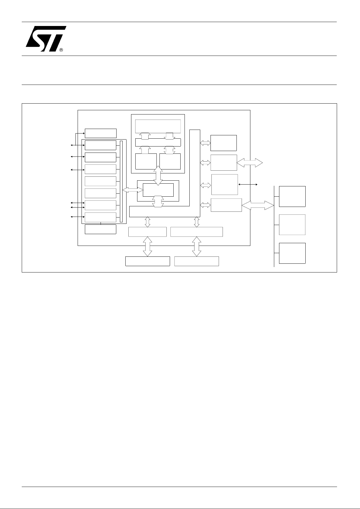
Figure 1
illustrates t he system architecture of the ST40 SH-4 core. The following section briefly
describes the features and performance of the core.
Central processing unit
The cen tr al processin g unit is built ar ound a 32-bit R IS C , two-way sup erscalar arc hitecture .
Operating at 166 MHz it runs with high code density using fixed length 16-bit instructions. It has a
load/store architec t ure, delayed branch ins t ruc t ion capabi lit y a nd an on-chi p m ult iplier. It uses a
five-stage pipeline.
Figure 1: ST40 SH-4 core architecture
CPU
UBC
FPU
ICache 8 Kbytes ITLB UTLB
Cache and TLB
controller
DCache 16 Kbytes
29bit add
32bit data
32bit data
32-bi t add (instruction)
32-b it data (instruction)
32-bit address (data)
32-bit data (load)
32-it data (store)
Lower 32-bit data
Lower 32-bit data
64-bit data (store)
Upper 32-bit data

ADCS 7260755H STMicroelectronics 8/94
ST40RA
4 Architect
ure
Floating point unit/m ultiply and accumulate
The on-c hip, floatin g point coproc essor exe cu t es s ingle precision (32-bit ) and double precision
(64-bit) operation s . It has a f iv e-stage pipeline and su pports IEEE 754-compliant data t yp es and
exceptions. It has rounding mo des: (round-t o-neares t ) and (round-t o-zero), and handles
denormalized nu m bers (trunc at ion-to-zero) or interru pt generation fo r c om pliance wit h I EEE754.
The floa ti ng point unit performs the following f unctions:
● fmac (multiply-and-accumulate), fdiv (divide),
● fsqrt (sq uare root) in s tr uc t ions,
● 3-D graphics ins tr uc t ions (single-precision):
➢ 4-dimens ional vecto r c onversion and matrix operations (ft rv ): 4 cycles (pitch), 7 cycles
(latency),
➢ 4-dimensional vector (fipr) inner product: 1 cycle (pitch), 4 cycles (latency).
MMU configuration
There is 4 Gbytes virtual address space with 256 address space identifiers (8-bit ASIDs),
support ing single virt ual and mu lti ple virtual me m ory modes . P age sizes are 1 Kbyte, 4 Kbyt es , 64
Kbytes or 1 Mbyte. The MMU supports four-entry, fully associative ITLB for instructions and
64-entry fully associative UTLB for instructions and operands. Software-controlled replacement and
random-counter replacement algori th m s are also supported. Th e physical ad dress space is 512
Mbytes (29-bit), see
Figure 2: System address organization on page 12
.
Cache
8 Kbyte s o f di rec t -m apped ins t ruc t ion cache are organiz ed as 256 32-b y t e lines, and 16 Kbytes of
direct-mapped operand cache are organized as 512 32-byte lines. RAM mode (8-Kbyte cache plus
8-Kbyt e R AM ) with sele ctable write m et hod (copy back or write t hrough) is supported . A sin gle
stage bu ffer f or c opy-back and a single st age buffer for writ e-through are availab le. T he c ache
conten ts c an be addres s m apped and t here is a 32-b yte two-entr y store queue.
4.2.2 SuperHyway internal interconnect
The ST4 0R A uses the SuperHyw ay m em ory mapped packet rout er for on-chip intermodule
communication. T he interconnect suppo rt s a s plit t ransaction system allowing a nonblocking high
throughput, low latency system to be built. There are separate request and response packet
routers.
The ST40RA SuperHyway implementation is show in
Section 5. 8: Memory bridge con t rol on
page 21
. The interconnect allows simultaneous requests between multiple modules and is able to
ensure a v ery high data through put with in many c as es zero rout ing, arbitrat ion and dec ode
latencies.
4.2.3 Standard ST40 peripherals
Synchronous serial channel
There are two ST40 co m patible full duplex com m unication c hannels (S C IF1, SCIF2).
Asynchronous mode is supported. A se parate 16-b y te F IFO is provided for the tra ns m it t er and
receive r.
Interrupt controller
The inte rrupt contro ller supports all of the on-c hip peripheral module int errupts, an d f iv e ex t ernal
interrupts (NMI and IRL0 to IRL3). The priority can be set for each on-chip pe ripheral mo dule
interrupt . IRL0 to IRL3 are configured as four independent interrupt s or encoded to prov ide 15
external interrupt levels.

4 Architect
ure
ST40RA
9/94 STMicroelectronics ADCS 7260755H
Debug controller
Debugging is performed by break interrupts. There are two break channels. The ad dress, data
value, access type, and data size can all be set as break conditions. Sequential break functions are
supported.
The user debug interface (UDI) contains a five-pin serial inte rfa c e c onforming t o J TAG, IEEE
Standard TA P and boundary scan a rc hit ecture. The interfac e provides hos t ac c es s t o t he 1 Kbyte
ASERAM for emu lat or firmware (ac c es s ible only in A SE mode).
Timers
The thre e-c hannel, a ut o-reload, 3 2-bit timer ha s an input capt ure function and a choice of s ev en
counter input clocks.
Real-time clock
The built -in 32-kHz cry s t al oscillator has a m aximum 1 /2 56 second res olution. It has dynam ic ally
progra m m able operat ing frequen c ies and on-ch ip c loc k and calend ar function s . It h as two sleep
modes and one standby mode.
Watchdog timer
The ST4 0R A has an 8-b it w at c hdog timer (W D T ) w it h program m able clock ra ti o. Th e W D T is able
to generate a power-on reset or a manual res et .
Programmable PLLs
The ST4 0R A has three program m able PLLs. T he PLLs are configured by M OD E pins at res et and
then reconfigured by software to optimize system performance or reduce system power
consumption.
General-purpose DMA controller
The five-c hannel phy s ic al address GPDMA c ont roller has four general-purpos e c hannels for
memory-to-memory or memory-to-peripheral transfers, and one buffered multiplexed channel. Both
2-D block moves and linked lists are suppor te d. Two sets of DMA handshake pins are available for
use by ext ernal devices to suppo rt effic ient transfer interdevic e transfers v ia external int erfaces
such as the EMI MPX.
Parallel I/O module
24 bits of parallel I/O are provided from t he ST40 com patible PIO. Eac h bit is program m able as an
output or an input. “Inp ut c om pare” generates an int errupt on a ny ch ange of any input bit.
4.3 Bus interfaces
4.3.1 Local memory interface
The LMI supports 16-, 3 2- a nd 64- bit wide bus SDRAM and DDR SDRAM, at up to 100 MHz with a
maximum address space of 112 Mbytes. Devices supported include two and four bank 16- , 64-,
128- an d 256-Mbit te c hnologies in x4 , x8 , x16 and x32 pac k ages. The LM I pads are dua l m ode
pads electrically compatible with L VTTL (for standard SDRAM) and SSTL_2 (for DDR SDRAM). For
full deta il of th e c onfiguration options of t he LMI pleas e s ee
ST40 System Architecture Manual,
Volume 2: Bus I nt erfaces
.

ADCS 7260755H STMicroelectronics 10/94
ST40RA
4 Architect
ure
4.3.2 PCI interface
The PCI interface co mplies to the
PCI v2.1
and
Power Management Interface V1.0
specifications. It
is 32 bits wide and operates at 33 or 66 MHz. Master and target mode are supported. A PCI arbiter
and clock generator is provided inside the ST40RA. For details on the configuration options for the
PCI interf ace please s ee
ST40 System Architecture Manual, Volume 2: Bus Interfaces
.
4.3.3 EMI/MPX interface
The EMI/MPX interface contains the fol lowi ng blo cks. Fo r full details of the configuration options of
the EMI please see the
ST40 System Architecture Manual, Volume 2: Bus Inter faces
.
EMI memory interface initiator
The EM I pr ov ides access t o R OMs, SDR AM , m em ory mapped asynch ronous ext ernal peripherals
and syn ch ronous MPX bus perip herals. The EM I s upports burs t m ode flash RO M and MPX for
memory-mapped device coupling. The ST40RA GPDMA unit accesses external devices and two
sets of DM A channel s co nt rol signals are provide d fo r t his purpose.
EMPI memory interface target
The EM PI is a synchrono us M PX target th at allows for an e x te rnal MPX initiator to access the
ST40R A internal memory spa c e. Th e EMPI con ta ins a general purpose cont rol channe l and four
high per fo rm ance channels each of which implements a w rit e buffer and a pair of 32-byte readahead buffers able to opt im iz e external device burs t ac c es s to and from the ST 40RA internal
memory. These buffers can be associated with memory regions within the S T40RA and external
DMA channels. Four sets of DMA handshake signals are provided to the EMPI to optimize long
burst transfers betw een the ST40RA and ex t ernal initiators like the S Ti5514 .
MPX bus arbiter
The ST4 0R A has an internal programmable bus arbiter to optimize utilizatio n of th e M PX bus. The
ST40RA MPX arbiter supports one external initiator and has programmable bus priority (ST40RA or
extern al device), bu s parking (ST40RA, external, idle o r las t us er) and laten c y timers. The in te rnal
arbiter c an be bypass ed if an exter nal arbiter supporting mo re initiators is required.
4.4 I/O devices
4.4.1 Mailbox
The ST4 0 and the ext ernal microprocesso r co m m unicate w ith each other and synchr onize their
activitie s us ing the mem ory -mappe d m ailbox. Proc es s es genera t e int errupts to e ith er CPU, and
send and receive messages between the two CPUs. There are buffers for message queueing in
both direc t ions and interrupt bits ca n be set in each direction. A c ce s s to the m ailbox from ex te rnal
device s is t hrough the ST 40RA EMPI or t he PCI targe t int erf ac e.
4.5 Software
4.5.1 Development systems and software
The ST4 0R A suppor ts application develop m ent, with a ful l range of deb ug f eatures and an
emulat ion mode (AS E). The ASE m ode has a d edicated 1-Kbyte buffer fo r em ulator firm w are,
support ing performance counters and branch trac e. T he ST40RA, w it h it s me m ory management
unit, supports standard operating systems including WindowsCE and Linux. The ST40 has a wide
range o f de v elopment s upport from ST and third par ti es , and efficiently ru ns applications written in
C, C++ and Java.

5 Syst
em configuration
ST40RA
11/94 STMicroelectronics ADCS 7260755H
ST’s own to ols inc lude:
● C/C++ compilers,
● debugger,
● proprietary OS.
Third parties include:
● Microsoft: WindowsCE,
● Sun: Jav aOS for cons umers,
● WindRiver: VxWorks, Tornado tools,
● Linux,
● Insignia JVM,
● ANT browser.
4.5.2 Software compatibility
SH-4 co r e so ftware
The ST4 0R A SH-4 core is binary co de compat ible with the Hit ac hi SH775 x family.
Standard peripheral driver
The ST4 0 s t andard SCIF, timer, re al-time clock and PIO are co m patible wit h th e ST40 SOC range
of devices and the Hitachi SH775x family.
Bus interface driver
The PCI, LMI, and EMI interfaces are register compatible with the ST40 SOC range of devices.
The ST40RA contains an EMPI and MPX arbiter and MPX clock control unit which are additional to
the bus in t erf ac e components of the ST 40 SOC ra nge of device s .
I/O device driver
The Mailbox is a module with no ST legacy software.
5 System configuration
The ST40RA system address map has been designed to maintain compatibility with existing ST40
family dev ic es and other STMicr oelectronic s dev ic es.
The SH-4 core and core peripherals maintain compatibility with the ST40 SOC range of devices and
Hitachi SH 7750 wh erever poss ible.
Devices listed in
Table 2: ST40RA system address map on page 13
, are doc um ented in the
ST40
System Architecture Manual
as described in
Chapte r 2: ST40 do cu m entation su it e on page 6
.
Coherency between the cache and external memory is assured by software. The ST40 CPU has
cache control instructions which enable software to do this. Details of these instructions are given in
the
ST40 CPU C ore Architecture Ma nual
.
The ST4 0R A is run in littl e endian mod e.
ADCS 7260755H STMicroelectronics 12/94
ST40RA
5 Syst
em configuration
The ST4 0R A power on c onf iguration is controlled by th e M ODE pins as defined in
Table 34: Mode
selection pins for ST 40RA on pa ge 59
.
Subsystem configuration registers are usually found with the module register space. Other system
level fun c ti ons and the sof tware register locations are shown in
Table 11 : S y stem config uration
registe rs on page 23
.
5.1 System addresses
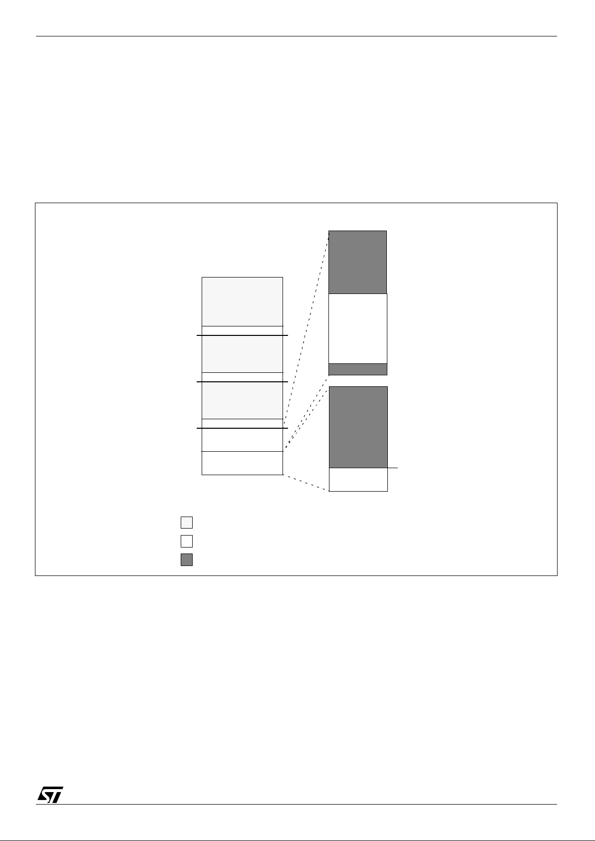
The ST40 family system address organization is shown in
Figure 2
.
Figure 2: System address organization
EMI
LMI
PCI
Area 7
Reserved
Core
Reserved
EMI control registers
LMI control registers
PCI control registers
Memory address space
Device control register address space
0x0000 0000
0x07F0 0000
0x0800 0000
0x0F00 0000
0x1000 0000
0x1700 0000
0x1800 0000
0x1C00 0000
0x1FFF FFFF
0x1800 0000
0x1C00 0000
0x1F00 0000
0x1FFF FFFF
Reserved
0x1BFF FFFF
System
0x1B00 0000
peripherals
peripherals
Reserved address space
(standard ST40
physical boot
address)
5 Syst
em configuration
ST40RA
13/94 STMicroel ec tronics ADCS 7260755H
5.1.1 System address map
Module
Address
a
Reference
Base Top
Standard bus interfaces
ST40 System Architect ure Manual Volume 2: Bus
Interfaces
EMI (FMI) 0x0000 0000 0x07EF FFFF
EMI control and buf fer
registers
0x07F0 0000 0x07FF FFFF
LMI 0x0800 0000 0x0EFF FFFF
LMI control registers 0x0F00 0000 0x0FFF FFFF
PCI 0x1000 0000 0x16FF FFFF
PCI control registers 0x1700 0000 0x17F F FFFF
Reserved 0x1800 0000 0x1AFF FFFF
ST40 core peripherals
ST40 System Architect ure Manual Volume 1: System
DMAC 0x1B00 0000 0x1B00 FFFF
PIO1 0x1B01 0000 0x1B01 FFFF
PIO2 0x1B02 0000 0x1B02 FFFF
PIO3 0x1B03 0000 0x1B03 FFFF
CLOCKGEN 0x1B04 0000 0x1B04 FFFF
Interconnect 0x1B05 0000 0x1B05 FFFF
Reserved 0x1B06 0000 0x1B0F FFFF
CLOCKGENB 0x1B10 0000 0x1B10 FFFF
Reserved 0x1B11 0000 0x1B12 FFFF
EMPI 0x1B13 0000 0x1B13 7FFF
ST40 System Architect ure Manual Volume 2: Bus
Interfaces
MPXARB 0x1B13 8000 0x1B13 FFFF
ST40 System Architect ure Manual Volume 2: Bus
Interfaces
ST40RA additional peri pherals
ST40 System Architecture Manual Volume 4: I/O
Devices
MailBox 0x1B15 0000 0x1B15 FFFF
SYSCONF 0x1B19 0000 0x1B19 FFFF
Reserved 0x1B1A 0000 0x1B1F FFFF
Reserved for additional peripherals
Reserved 0x1B20 0000 0x1B3F FFFF
ST40 core peripherals
ST40 System Architect ure Manual Volume 1: System
INTC2 0x1E08 0000 0x1E0F FFFF
Table 2: ST40RA system address map
ADCS 7260755H STMicroelectronics 14/94
ST40RA
5 Syst
em configuration
5.2 System identifiers
● SH-4 c ore process or identity: 0x 0100.
● SH-4 c ore process or version: 0x 0541D.
● ST40RA-HC8 TAP identity: 0514104 1.
● ST40RA-HC8 PCI identity:
➢ Vendor: 104A,
➢ Device: 4000,
➢ Revision ID: 0x01,
➢ Class: 0x4 0000,
➢ Subsystem ID: 0x0000.
Reserved: CPU only
registers
0x1E10 0000 0x1FBF FFFF
CPG 0x1FC0 0000 0x1FC7 9999
RTC 0x1FC8 0000 0x1FCF FFFF
INTC 0 x1FD0 0000 0x1FD7 9999
TMU 0x1FD8 0000 0x1FDF FFFF
SCIF1 0x1FE0 0000 0x1FE7 9999
SCIF2 0x1FE8 0000 0x1FEF FFFF
EMU 0x1FF0 0000 0x1FF7 9999
Reserved 0x1FF8 0000 0X1FFF FFFF
a. For information about which address region to access for each module, see
SH-4 32-bit CPU Core
Architecture, sections 2.5 and 3.4
.
When operating in privilege mode, these registers should be accessed via the P2 region by adding
an offset of 0xA000 0000, when operating in user mode, access should be via the U0 address.
Module
Address
a
Reference
Base Top
Table 2: ST40RA system address map
5 Syst
em configuration
ST40RA
15/94 STMicroel ec tronics ADCS 7260755H
5.3 Interrupt mapping
For full de t ails on the interrupt contro ller see
ST40 System Architecture Manual Volume 1:System
.
The map ping of the CP U int errupts is d es c ribed in
Section 5. 3.1, Sectio n 5.3.2
and
Section 5.3.3
.
Note: Some INTEVT c odes are shown as res erv ed in Table 3 and therefore cannot be generated by this
device.
5.3.1 ST40 core interrupt allocation
The alloc at ion of core int errupts is as s hown in
Table 3
.
Interrupt source
INTEVT
code
Interrupt priority
IPR
bit numbers
Priority
within IPR
setti ng unitValue Initial value
NMI 0x1C0 16 - - IRL
level
encoding
IRL3–IRL0 = F 0x200 15 - - IRL3–IRL0 = E 0x220 14 - - IRL3–IRL0 = D 0x240 13 - - IRL3–IRL0 = C 0x260 12 - - IRL3–IRL0 = B 0x280 1 1 - - IRL3–IRL0 = A0x2A0 10 - - IRL3–IRL0 = 90x2C0 9 - - IRL3–IRL0 = 80x2E0 8 - - IRL3–IRL0 = 7 0x300 7 - - IRL3–IRL0 = 6 0x320 6 - - IRL3–IRL0 = 5 0x340 5 - - IRL3–IRL0 = 4 0x360 4 - - IRL3–IRL0 = 3 0x380 3 - - IRL3–IRL0 = 20x3A0 2 - - IRL3–IRL0 = 10x3C0 1 - - -
IRL
independent
encoding
IRL0 0x240 15 to 0 13 IPRD[15:12] IRL1 0x2A0 15 to 0 10 IPRD[11:8] IRL2 0x300 15 to 0 7 IPRD[7:4] -
IRL3 0x360 15 to 0 4 IPRD[3:0] H-UDI H-UDI 0x600 15 to 0 0 IPRC[3:0] TMU0 TUNI0 0x400 15 to 0 0 IPRA[15:12] TMU1 TUNI1 0x420 0 to 15 0 IPRA[11:8] TMU2 TUNI2 0x440
0 to 15 0 IPRA[7:4]
High
TICPI2 0x460 Low
Table 3: ST40 core interrupt allocation (page 1 of 2)

ADCS 7260755H STMicroelectronics 16/94
ST40RA
5 Syst
em configuration
5.3.2 ST40 standard system interrupt allocation
Standard ST40 fam ily interrupt s are mappe d as s hown in
Table 4
.
RTC ATI 0x480
0 to 15 0 IPRA [3:0]
High
to
low
PRI 0x4A0
CUI 0x4C0
SCIF1 ERI 0x4E0
0 to 15 0 IPRB[7:4]
High
to
low
RXI 0x500
BRI 0x520
TXI 0x540
SCIF2 ERI 0x700
0 to 15 0 IPRC[7:4]
High
to
low
RXI 0x720
BRI 0x740
TXI 0x760
WDT ITI 0x560 0 to 15 0 IPRB[15:12] -
Interrupt source
INTEVT
code
Interrupt priority
IPR
bit numbers
Priority
within IPR
setti ng unitValue Initial value
PCI PCI_SERR_I N T 0xA00
0 to 15 0
INTPRI00[0:3]
INTPRI00[7:4]
High to low
PCI_ERR_INT 0xA20
High
to
low
PCI_AD_INT 0xA40
PCI_PWR_DWN 0xA60
Reserved
DMAC DMA_INT0 0xB00
0 to 15 0 INTPRI00[11:8]
High
to
low
DMA_INT1 0xB20
DMA_INT2 0xB40
DMA_INT3 0xB60
DMA_INT4 0xB80
Reserved
DMA_ERR 0xBC0
PIO0 PIO0 0xC00 0 to 15 0 INTPRI00[15:12] PIO1 PIO1 0xC80 0 to 15 0 INTPRI00[19:16] PIO2 PIO2 0xD00 0 to 15 0 INTPRI00[23:20] -
Table 4: ST40 stand ard interrupt allocation
Interrupt source
INTEVT
code
Interrupt priority
IPR
bit numbers
Priority
within IPR
setti ng unitValue Initial value
Table 3: ST40 core interrupt allocation (page 2 of 2)
5 Syst
em configuration
ST40RA
17/94 STMicroel ec tronics ADCS 7260755H
5.3.3 ST40RA I/O device interrupt allocation
5.4 GPDMA channel mapping
For full de t ails of t he GPDMA c ontroller see
ST40 System Architecture Manual Volume 1: System
.
The ST4 0R A general purpose DM A controller channe l m ap is shown in
Table 6
.
Interrupt source
INTEVT
code
Interrupt priority
IPR
bit numbers
Priority
within IPR
setti ng unitValue Initial value
Mailbox MAILBOX 0x1000
0 to 15 0 INTPRI04[0:3] High to low
Reserved
Reserved
0 to 15 0 INTPRI04[27:24] High to low
EMPI INV_ADDR 0x1380 0 to 15 0 INTPRI04[31:28] High to low
Reserved
Ta ble 5: Mailbox and EMPI interru pt allocation
Request
number
Associated
device
Protocol Comme nt
0 External device 0 DREQ or
DREQ/DRACK
The following pins are available for external peripherals:
DREQ[0:1],
DACK[0:1],
DRAK[0:1].
1 External device 1 DREQ or
DREQ/DRACK
2 and 3 Reserved
4 SCIF1 trans mit DREQ
This allow SCIF to memory and memory t o SCIF transfer
to be supported on any DMA channel.
5 SCIF1 received DREQ
6 SCIF2 trans mit DREQ
7 SCIF2 receive DREQ
8 TMU DREQ/DRACK Typical ly used to trigger or pac e memory tr ansfers.
9 and 10 Reserved
1 1 PCI1 DREQ or
DREQ/DRACK
May be used to improve the efficiency of transfers to and
from the PCI.
12 PCI2 DREQ or
DREQ/DRACK
13 PCI3 DREQ or
DREQ/DRACK
14 PCI4 DREQ or
DREQ/DRACK
15 to 31 Reserved
Table 6: GPDMA request numb er allocation
ADCS 7260755H STMicroelectronics 18/94
ST40RA
5 Syst
em configuration
5.5 EMI DACK mapping
For full details of the EMI bank address and bank type mappings refer to
ST40 Sy st em Ar ch it ect ur e
Manual Volum e 2: Bus Interf aces.
Two DACK strob es are suppor te d in t his implem entation and are mapp ed as follows:
● DACK [0]: asserted w hen a transf er f rom GPDM A c hannel[1] oc c urs to an EMI bank configu red
as a MPX de v ic e,
● DACK [1]: asserted w hen a transf er f rom GPDM A c hannel[2] oc c urs to an EMI bank configu red
as a MPX de v ic e.
5.6 EMI address pin mapping
The data width of a connected device is 8, 16 or 32 bits wide. The 16-bit bank must use EDQM3 as
address 1, th e LSB addres s f or t he device and the 8-bit bank must us e EDQM3 as address 1 and
EDQM 2 as address 0.
See the
ST40 System Architecture Manual, Volume 2: Bus In terfaces
for details of setting the
device type and port size using the EMI configuration reg is t ers .
Device type Port size Device address 25 to 2 Device address 1 Device address 0
SDRAM
Peripheral
SFlash
32-bit EADDR[25:2] - 16-bit EADDR[24:2] EDQM 3 8-bit EADDR[23:2] EDQM3 EDQM2
MPX - EADDR[25:2] - -
Table 7: Mapping the internal address lines of a connecte d device

5 Syst
em configuration
ST40RA
19/94 STMicroel ec tronics ADCS 7260755H
5.7 EMI pin to function relationship
ST40RA EMI pin Peripheral SFlash SDRAM MPX MPX/EMPI
EADDR[2:26] MEM_ADDRESS MEM_ADDRESS MEM_ADDRESS - EADDR3 NOT_CS - - CLK CLK
EADDR4 NOT_OE - - /CS /CS
EADDR5 NOT_BE - - /FRAME /FRAME
EADDR6 MEM_DATA - - /BS /BS
EADDR7 (write) - - /WE /WE
EADDR8 MEM_DATA - - I/O [31:0] I/O [31:0]
EADDR9 (read) - - I/O [63:61] I/O [63: 61]
EDA TA[0:31] MEM_DATA MEM_DATA MEM_DATA MEM_DATA[31:0] MEM_DATA[31:0]
ECLKOUT - - SDRAMCLOCK - ECLKEN - - CKEN - -
EDQM0 NOT_BE0 NOT_BE0 NOT_MEMBE0 - EDQM1 NOT_BE1 NOT_BE1 NOT_MEMBE1 - EDQM2 NOT_BE2 NOT_BE2 NOT_MEMBE2 - EDQM3 NOT_BE3 NOT_BE3 NOT_MEMBE3 - NOTECS0 NOT_CS0 NOT_CS0 NOT_SDRAMCS0 NOT_CS0 NOTEMPICS0
NOTECS1 NOT_CS1 NOT_CS1 NOT_SDRAMCS1 NOT_CS1 NOTEMPICS1
NOTECS2 NOT_CS2 NOT_CS2 NOT_SDRAMCS2 NOT_CS2 NOTEMPICS2
NOTECS3 NOT_CS3 NOT_CS3 NOT_SDRAMCS3 NOT_CS3 NOTEMPICS3
NOTECS4 NOT_CS4 NOT_CS4 - NOT_CS4 NOTEMPICS4
NOTECS5 NOT_CS5 NOT_CS5 - NOT_CS5 NOTEMPICS5
NOTERAS - NOT_ADDRVALID NOT_MEMRAS NOT_BS NOT_BS
NOTECAS NOT_OE NOT_OE NOT_MEMCAS NOT_FRAME NOT_FRAME
EWAIT MEM_WAIT MEM_WAIT - MEM_WAIT MEM_WAIT
NOTEWE READNOTWRITE READNOTWRITE READNOTWRITE READNOTWRITE READNOTWRITE
EPENDING
a
RFSH_PENDING
or ACC_PENDING
(master )
ACC_PENDING
only (slave)
RFSH_PENDING
or ACC_PENDING
(master )
ACC_PENDING
only (slave)
RFSH_PENDING
or ACC_PENDING
(master)
ACC_PENDING
only (slave)
RFSH_PENDING
or ACC_PENDING
(master)
ACC_PENDING
only (slave)
RFSH_PENDING
or ACC_PENDING
(master )
ACC_PENDING
only (slave)
MCLKOUT - - - MPX clock MPXCLOCK
NOTMREQ (slave) EMI_HOLD_REQ EMI_HOLD_REQ EMI_HOLD_REQ - NOTMREQ
(master)
EMI_BUS_REQ EMI_BUS_REQ EMI_BUS_REQ MPX bus request MPX bus request
NOTMACK (slave) EMI_HOLD_ACK EMI_HOLD_ACK EMI_HOLD_ACK - -
Table 8: EMI pi n func ti ons

ADCS 7260755H STMicroelectronics 20/94
ST40RA
5 Syst
em configuration
NOTMACK
(Master)
EMI_BUS_GRANT EMI_BUS_GRANT EMI_BUS_GRANT MPX bus
acknowledge
MPX bus
acknowledge
FCLKOUT - FLASHCLOCK - - NOTFBAA - Unconnected/
connected
b
---
NOTESCS0 - - - - MBXINT
NOTESCS1 - - - - EMPIDREQ0
NOTESCS2 - - - - EMPIDRAK0
a. When the EMI is configured in master mode (MODE9 = H), and an external slave DMA asks for
access to the bus (using NOTMACK or NOTMREQ), RFSH_PENDING and ACC_PENDING are
used to signal that, while the external DMA request has been granted and the DMA is using the bus,
a refresh time out occurred, or that the EMI has been asked for a new access. A bus arbiter, if
present, can use this information to give back the bus to the EMI to allow a re fresh operation, or
improve bandwidth. When the EMI is in slave mode (MODE9 = L), RFSH_PENDING is always
deasserted (so EPENDING = ACC_PENDING), and the pin is used to signal to the external bus
arbiter that the EMI needs to use the bus.
b. NO TFBAA is an output of the ST40RA, and an input to the memory device. The pin must be left
unconnected from the ST40RA side and tied low at the memory device side if the memory is an Intel
or an STM part. It needs to be connected if the SFlash is an AMD.
ST40RA EMI pin Peripheral SFlash SDRAM MPX MPX/EMPI
Table 8: EMI pi n func ti ons
5 Syst
em configuration
ST40RA
21/94 STMicroel ec tronics ADCS 7260755H
5.8 Memory bridge control
The architecture of the SuperHyway interconnect is shown in
Figure 3
. Initiato rs are shown on t he
left, and targets are shown on the right of the interconnect. The bit width of the initiator and target
ports are s how n in the diag ram.
The ST4 0R A architec t ure requires se v en memory bridges on cloc k c hange boundaries.
Figure 3: ST40RA interconnect architecture
Memory bridge number SuperHyway type Subsystem
1 T3 EMI target
2 T3 EMPI initiator
3 T1 EMI_SS target
4 T2 Reserved
5 T2 Reserved
6T3PCI_ST_I
7T3PCI_ST_T
Table 9: Memo ry bridges
SuperHyway
Interconnect
SH core
EMPI
PCI_ST_I
LMI
EMI
PCI_ST_T
Memory
bridge
Memory
bridge
Memory
bridge
Memory
bridge
P
I
PER
SH_PER
32
32
32
GPDMA
32
64
32
32
32
ADCS 7260755H STMicroelectronics 22/94
ST40RA
5 Syst
em configuration
5.8.1 Memory bridge control signals
Each me m ory bridge has s ev en control s ignals as def ined in
Table 10
.
5.8.2 Memory bridge status
The memory bridge control signals are looped back to the ST40RA comms subsystem SYS_STAT1
registe r fo r t es t purposes. The format o f this read-only register is show n in
Section 5.9.4.1:
SYSCONF.SYS_STAT1. on page 26
.
5.8.3 Changing control of a memory bridge
At reset all these bridges are set to be synchronous. After reset and boot the function of these
memor y bridges can be changed . See
Section 5.9.4: SYSCONF registers on page 26
. The
procedure for changing the control of a me m ory bridge is g iv en below.
1 Ensure no init iat ors are acc es s ing the subs yst em the bridge is connec t ed to and ensure the
subsystem cannot init iate any requests to the SuperHyway.
2 Stop the clock to the subsystem.
3 Change the memory bridge configuration using the SYS_CONF.SYS_CON1 register as
detailed in
Table 10
.
4 Restart the clock to the subsystem and reinitialize the system.
Bridge control bit field Control name Control function
1:0 MODE[1:0] 00: Sync (bypass) bridge
01: Semisync with no retime registers
10: Semisync with one ret ime register
11: Async with two retime registers
4:2 LATENCY[2:0] Sets FIFO latency from 0 to 7 cycles.
5 SW_RESET 0: Software reset inactive
1: Software reset active
6 STROBE The above control signals are latched in the bridge on the rising
edge of this strobe bit
Tab le 10: Memory b rid ge co ntrol signal s
5 Syst
em configuration
ST40RA
23/94 STMicroel ec tronics ADCS 7260755H
5.9 System configuration registers
Table 11
outlines the ST40RA system configuration registers.
Register Module
Address
offset
Type Description
EMI.GENCFG EMI 0x028 R/W EMI general purpose configuration register, see
Section 5.9.1: EMI.GENCFG EMI gener al
configuration on page24
LMI.COC LMI 0x028 R/W LMI clock and pad control register, see
Section 5.9.2: LMI.COC on page 25
LMI.CIC LMI 0x040 RO LMI clock and pad status, see
Section5.9.3:
LMI.CIC on page 26
SYS_STAT1 SYSCONF 0x040 RO Memory bridge status , see
Section 5.9.4.1:
SYSCONF.SYS_STAT1. on page 26
SYSCONF.SYS_CON1 SYSCONF 0x010 R/W System configuration register, see
Section 5.9.4.2: SYSCONF.SYS_CON1. on
page 27
SYSCONF.SYS_CON2 SYSCONF 0x018 R/W System configuration register, see
Section 5.9.5:
SYSCONF.SYS_CON2. on page 27
SYSCONF.CNV_STATUS SYSCONF 0x020 R/W System configuration register, see
ST40 System
Architecture Manual Volume 4: I/O Devices
SYSCONF.CNV_SET SYSCONF 0x028 R/W System configuration register, see
ST40 System
Architecture Manual Volume 4: I/O Devices
SYSCONF.CNV_CLEAR SYSCONF 0x030 R/W System configuration register, see
ST40 System
Architecture Manual Volume 4: I/O Devices
SYSCONF.CNV_CONTROL SYSCONF 0x038 R/W System configuration register, see
ST40 System
Architecture Manual Volume 4: I/O Devices
Table 1 1: System configuration registers

ADCS 7260755H STMicroelectronics 24/94
ST40RA
5 Syst
em configuration
5.9.1 EMI.GENCFG EMI general configuration
EMI.GENCFG EMI general configuration 0x0028
The EM I pr ov ides a gene ric register to al low t he configuration of the padlogic. ST 40RA
uses the bits detaile d.
0SOFE Strobe positioning
Strobe on falling edge:
0: Disabled
1: Enabled
Rese t: 0
RW
[5:1] SDPOS SDRAM bank location
00001: Bank 0 00010: Bank 1
0001 1: Bank 2 00100: Bank 3
00101: Bank 4 00110: Bank 5
10001: Bank 0 to 1 10010: Bank 0 to 2
1001 1: Bank 0 to 3 10100: Bank 0 to 4
10101: Bank 0 to 5 10110: Bank 1 to 2
101 11: Bank 1 to 3 11000: Bank 1 to 4
1 1001: Bank 1 to 5
11010: Ba nk 2 t o 3
1 1011: Bank 2 to 4 1110 0: Bank 2 to 5
1 1101: Bank 3 to 4 11110: Bank 3 to 5
11111: Bank 4 to 5
Rese t: 0
RW
6EWPU
Pull-up on EWAI T pin
a
0: Disabled
1: Enabled
Rese t: 0
a. If the EWAIT signal is set at the beginning of an access, and the data is to be set after the EWAIT
is cleared, the parameters ACCESSTIMEREAD and LATCHPOINT in the EMI configuration
registers must be set as follows:
ACCESSTIME > LATCHPOINT + 3.
See the
ST40 System Architecture Manual, Volume 2: Bus Interfaces
for details of setting the EMI
configuration registers.
RW
7 EAPU Pull-up enable on EADDR pins
0: Disabled
1: Enabled
Rese t: 0
RW
[31:8] Reserved 0: Ignored
1: Reserved
Reset: Undefined

5 Syst
em configuration
ST40RA
25/94 STMicroel ec tronics ADCS 7260755H
5.9.2 LMI.COC
LMI.COC LM I cl ock and pad control 0x028
LMI.COC allows modific ati on of the glue logic.
0 DLY_SRC Delay line control source
0: DLL provides delay line control
1: LMI.CFG[5:1] provides delay line control
Rese t: 0
RW
[5:1] DLY_NUM Number of delays (~200ps each)
Rese t: 0
RW
[7:6] DLY_FRQ_RES External delay frequency resolution
Rese t: 0
RW
19:8] PLL_SETUP PLL setup
Rese t: 0
RW
[21:20] DLL_PRO_CON DLL programmer control
Rese t: 0
RW
22 FRQ_RES_SRC Frequency resolution source of external delay
0: DLL provides frequency resolution
1: LMI.CFG[7:6] provides frequency resolution
Rese t: 0
RW
23 PLL_SETUP PLL setup
Rese t: 0
RW
24 DLL_PRO_SRC DLL programmer source
0: Delay programmer bl ock provides DLL programming
1: LMI.CFG[21:20] provides DLL programming
Rese t: 0
RW
[30:25] Reserved
31 DLL_ENB DLL enable
Rese t: 0
RW
ADCS 7260755H STMicroelectronics 26/94
ST40RA
5 Syst
em configuration
5.9.3 LMI.CIC
5.9.4 SYSCONF registers
All ST40 systems contain a number of general purpos e configurat ion registers which may be used
to configure system logic.
The def init ion of the general regis te rs and their acc es s fu nc t ions is defin ed in the
ST40 System
Architecture Manual.
For ST4 0R A the bits wit hin these regis t ers have th e fo llowing func t ion.
5.9.4.1 SYSCONF.SYS_STAT1.
LMI.CIC LMI clock and pad status
0x040
LMI.CIC reflects the status of the glue logic.
[4:0] DLY_STATE DLL delay state RO
5 DLL_LOCK DLL lock signal RO
6 PLL_LOCK PLL lock signal RO
[8:7] DLL_STATE DLL state RO
[21:9] PLL_SETUP_STATE PLL setup state RO
[24:22] DLL_SETUP_STATE DLL setup state RO
[26:25] DLL_BYPASS DLL bypass state RO
[31:27] LMI_SETUP LMI.CFG setup for external delay RO
SYS_STAT1 Memory bridge status 0x0040
[3:0] Reserved
[10:4] STATUS1 Status memory bridge 1 RO
[17:11] STATUS2 Status memory bridge 2 RO
[24:18] STATUS3 Status memory bridge 3 RO
[31:25] STATUS4 Status memory bridge 4 RO
[38:32] STATUS5 Status memory bridge 5 RO
[45:39] STATUS6 Status memory bridge 6 RO
[52:46] STATUS7 Status memory bridge 7 RO
[63:53] Reserved
5 Syst
em configuration
ST40RA
27/94 STMicroel ec tronics ADCS 7260755H
5.9.4.2 SYSCONF.SYS_CON1.
Where the two clocks are sourced from independent PLLs the br idge must be put in asynch ronous
mode.
5.9.5 SYSCONF.SYS_CON2.
SYSCONF.SYS_CON1 Memory bridge control 0x010
[3:0] Reserved RW
[10:4] MB1 Memory bridge 1 control: EMI target RW
[17:11] MB2 Memory bridge 2 control: EMPI initiator RW
[24:18] MB3 Memory bridge 3 control: EMI_SS target RW
[38:25] Reserved
[45:39] MB6 Memory bridge 6 control: PCI initiator RW
[52:46] MB7 Memory bridge 7 control: PCI target RW
[63:53] Reserved
SYSCONF.SYS_CON2 Functional pin use and behavior 0x0018
The SYSCONF.SYS_CON2 register controls functional pin use and behavior
8LMI_MODE
LMI pad type
0: SSTL
1: LVTTL
Reset: 0
RW
9 LMI_ENVREF
Reference voltage source
0: internally generated reference voltage
1: external reference voltage from VREF pins
Reset: 0
RW
10 LMI_ECLK_BYPASS
LMI control signal ECLK180 retime bypass
0: ECLK180 flip flop not by passed
1: ECLK180 flip flop is bypassed
Reset: 0
RW
11 LMI_NOTCOMP25_EN
Enable LMI 2.5 V compensation cell
0: LMI 2.5 V compensation cell enabled
1: LMI 2.5 V compensation cell disabled
Reset: 0
RW
12 LMI_COMP33_EN
Enable LMI 3.3 V compensation cell
0: LMI 2.5 V compensation cell enabled
1: LMI 2.5 V compensation cell disabled
Reset: 0
RW

ADCS 7260755H STMicroelectronics 28/94
ST40RA
5 Syst
em configuration
[13:14] LMI _SDRAM_DATA_DRIVE
SDRAM data and data strobe pad PROG 1:0 L VTTL
OP drive strength
00: 1x
01: 2x
10: 3x
11 : 4x
Reset: 0
RW
[15:16] LMI _SDRAM_ADD_DRIVE
LMI address and control pad PROG 1:0 LVTTL OP
drive strength
00: 1x
01: 2x
10: 3x
11 : 4x
Reset: 0
RW
[17:35] Reserved
36 EMPI_ENB[0]
Enable EMPI channel 0 DREQ/DRACK/DRACK
alternate function
0: Disabled
1: NOTESCS1 remapped to EMPIDREQ0
NOTESCS2 remapped to EMPIDRAK0
EADDR26 remapped to EMPIDACK0
EADDR26 is only remapped when whilst the ST40RA
is acting as a bus slave
RW
37 EMPI_ENB[1]
Enable EMPI channel 1 DREQ/DRACK/DRACK
alternate function
0: Disabled
1: NOTPREQ3 remapped to EMPIDREQ1
NOTPGNT3 remapped to EMPIDRAK1
EADDR25 remapped to EMPIDACK0
EADDR25 is only remapped when whilst the ST40RA
is acting as a bus sla ve
RW
38 EMPI_ENB[2]
Enable EMPI channel 2 DREQ/DRACK/DRACK
alternate function
0: Disabled
1: DREQ0 remapped to EMPIDREQ2
DACK0 remapped to EMPIDACK2
DRAK0 remapped to EMPIDRAK2
RW
39 EMPI_ENB[3]
Enable EMPI channel 2 DREQ/DRACK/DRACK
alternate function
0: Disabled
1: DREQ1 remapped to EMPIDREQ3
DACK1 remapped to EMPIDACK3
DRAK1 remapped to EMPIDRAK3
RW
40 MAILBOX_ENB
Enable mailbox interrupt alternate function
0:Disabled
1:NOTESC0 remapped to MBXINT
RW
[41:43] R eserved
SYSCONF.SYS_CON2 Functional pin use and behavior 0x0018
5 Syst
em configuration
ST40RA
29/94 STMicroel ec tronics ADCS 7260755H
5.9.6 PIO alternate functions
The fun ction of pads w it h PI O alternate function s are c ontrolled by th e PI O.PC0, PIO.PC1 and
PIO.PC2 registers .
In the ST40RA devic e, the operat ional mod es fo r t hes e registers differ from the st andard
archite c tu re definition and are sho w n in
Table 12
.
[44:46] EM PI_CS_ENB
Enable EMPI chip selection alternate function
000: NOTESC0 remapped to NOTEMPICS
001: NOTESC1 remapped to NOTEMPICS
010: NOTESC2 remapped to NOTEMPICS
011: NOTESC3 remapped to NOTEMPICS
100: NOTESC4 remapped to NOTEMPICS
101: NOTESC5 remapped to NOTEMPICS
110: Reserved
1 11: Disabled (val ue at reset)
RW
47 SEL_EXT_EMI_SLAVE
Select EMI slave or master functionality
0: EMI is bus master
1: EMI is bus slave
RW
[48:59] Reserved
[60:63] PIO_CONF PIO_CONF RW
PIO bi t configur a tion PIO out put state PI O.PC2 PIO.PC 1 PIO.PC0
NonPIO function
a
a. State following reset
-000
PIO bidirectional Open drai n 0 0 1
PIO output Push-pull 0 1 0
PIO bidirectional Open drai n 0 1 1
PIO input Hi gh impedance 1 0 0
PIO input Hi gh impedance 1 0 1
Reserved - 1 1 0
Reserved - 1 1 1
Table 12: PIO alternate function registers
SYSCONF.SYS_CON2 Functional pin use and behavior 0x0018
 Loading...