

■ SUPPLYVOLTAGERANGE4.5VTO5.5V
■ MINIMUM DIFFERENTIAL INPUT VOLTAGE
± 200mV
■ TYPICAL PROPAGATION DELAYS: 19ns
■ TYPICAL INPUT HYSTERESIS: 60mV
■ INPUT RESISTANCE 10KΩ
■ OPEN INPUT FAIL SAFE FEATURE
■ OPERATING TEMPERATURE RANGE
-40°C TO 85°C
DESCRIPTION
The ST34C86 is a quad differential li ne receiver
designed to meet the RS-422, RS-423, and
Federal Standard 1020 and 1030 for balanc ed
and unbalanced digital data transmission, while
retaining the low power characteristics of CMOS.
The ST34C86 has an input sensivity of 200mV
over the common mode input voltage range of
±7V. Hysteresis is provided to improve noise
ST34C86
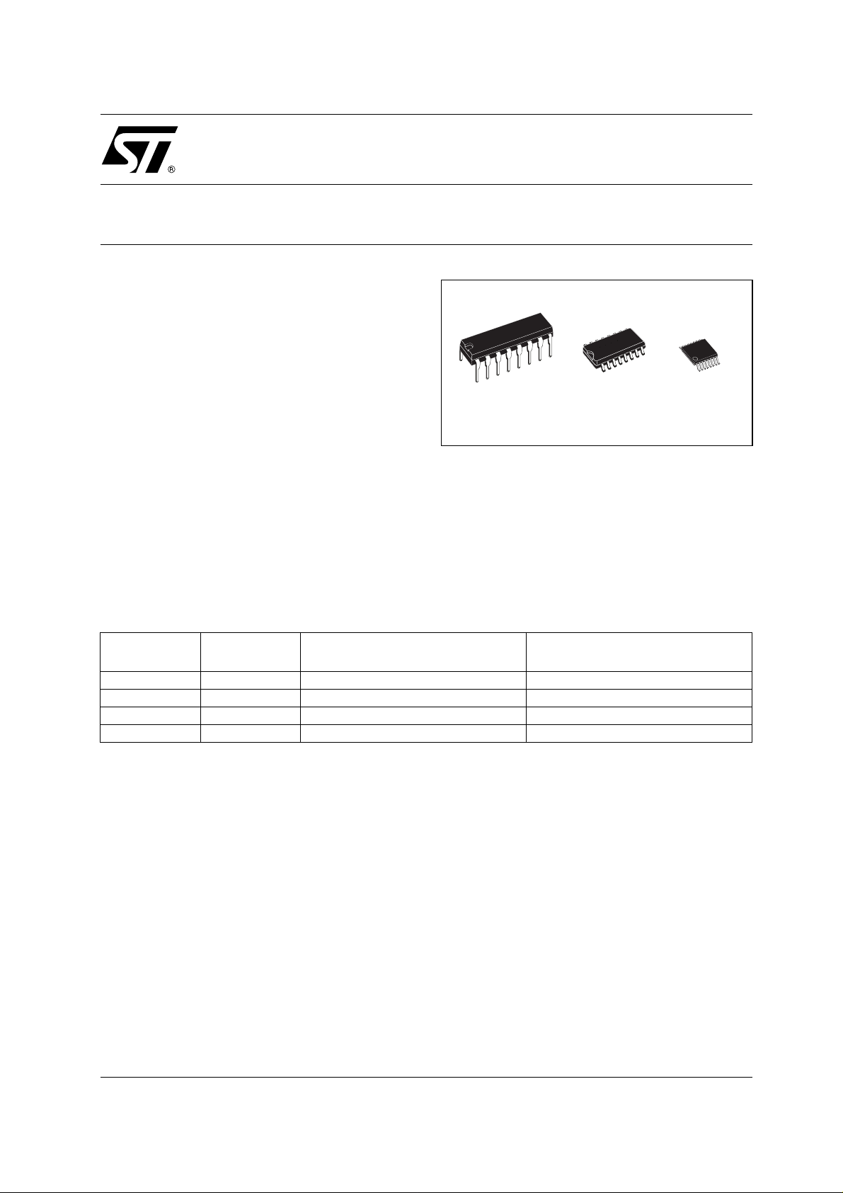
CMOS QUAD 3-STATE
DIFFERENTIAL LINE RECEIVER
DIP SOP TSSOP
margin and discourage output instability for slowly
changing input waveforms. The ST34C86 internal
pull-up and pull-down resistors. prevent output
oscillation on unused channels. Separate enable
pins allow independent control of receiver pairs.
The 3-STATE outputs have 6mA sourc e and sink
capability.
ORDERING CO DE S
Type
ST34C86BN -40 to 85 °C DIP-16 25parts per tube / 40tube per box
ST34C86BD -40 to 85 °C SO-16 (Tube) 50parts per tube / 20tube per box
ST34C86BDR -40 to 85 °C SO-16 (Tape & Reel) 1000 parts per reel
ST34C86BTR -40 to 85 °C TSSOP-16 (Tape & Reel) 2500 parts per reel
Temperature
Range
Package Comments
1/10September 2002
ST34C86
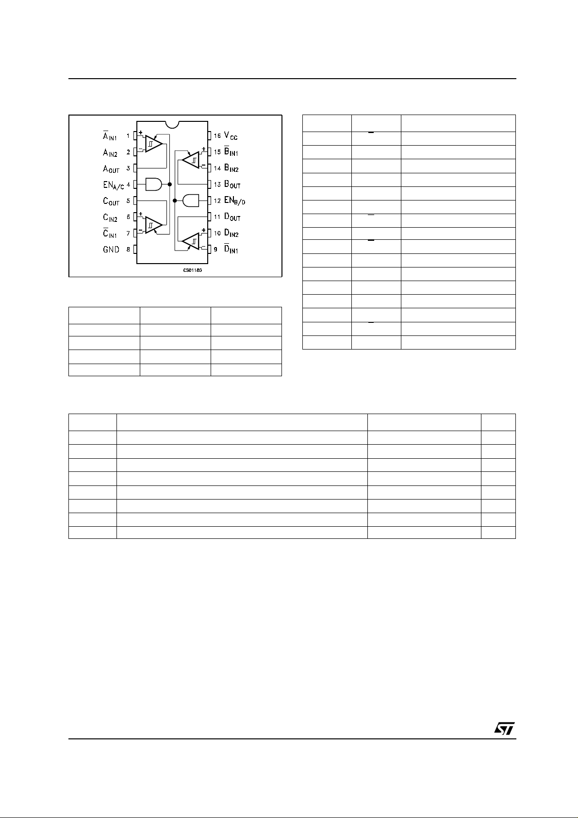
PIN CONFIGURATION
TRUTH TABLE
Enable Input Output
LXZ
≥ VTH(Max)
H
H
V
ID
≤ VTH(Min)
V
ID
H Open * H
X= Don’t Care; Z=High Impedance, * Open=Not terminated
H
L
PIN DESCRIPTION
PlN N° SYMBOL NAME AND FUNCTION
1
2
3
4
5
6
7
A
A
A
EN
C
C
C
IN1
IN2
OUT
OUT
IN2
IN1
8 GND Ground
9
10
11
12
13
14
15
16
D
D
D
EN
B
B
B
V
IN1
IN2
OUT
OUT
IN2
IN1
CC
Input A1
Input A2
Channel A Output
Enable A/C
A/C
Channel C Output
Input C2
Input C1
Input D1
Input D2
Channel D Output
Enable B/D
B/D
Channel B Output
Input B2
Input B1
Supply Voltage
ABSOLUTE MAXIMUM RATINGS
Symbol Parameter Value Unit
V
V
V
DIFF
V
I
OUT
T
T
ESD HBM (1.5KΩ 100pF) 2000 V
Absolute Maximum Ratings are those values beyond which damage to the device may occur. Functional operation under these condition is
not implied.
Unless otherwise specified, all voltage are referenced to ground.
ESD Rating:HBMInputs ≥
Supply Voltage
CC
Input Common Mode Range
CM
Differential Input Voltage
Enable Input Voltage
IN
Current per Output
Storage Temperature Range
stg
Operating Junction Temperature Range
op
2000V, All other pins ≥ 1000V , EIAJ(0Ω, 200pF) ≥ 350V
7V
± 14 V
± 14 V
7V
± 25 mA
-65 to 150 °C
-40 to 85 °C
2/10
ST34C86
DC ELECT RICAL CHARACTERISTICS
(V
=5V± 10%,TA= -40°C to 85°C , unless otherwise specified. Ty pical v alues arereferred to VCC=5V,
CC
= 25°C)
T
A
Symbol Parameter Test Conditions Min. Typ. Max. Unit
V
R
V
V
V
I
V
HYST
Minimum Differential Driver
TH
Input Voltage
Input Resistance VIN= -7V to +7V Other Input = GND 5 6.8 10 KΩ
IN
Input Current (under test) VIN= +10V Other Input = GND
I
IN
High Level Output Voltage VCC= Min V
OH
Low Level Output Voltage VCC= Min V
OL
Minimum Enable High Input
IH
Voltage
Minimum Enable Low Input
V
IL
Voltage
I
Maximum 3-STATE Output
OZ
Leakage Current
Maximum Enable Input
I
I
Current
Quiescent Power Supply
CC
Current
Input Hysteresis VCM=0V 60 mV
VO=VOHor V
VCM= -7V to +7V -200 35 200 mV
OL
1.1
V
= -10V Other Input = GND
IN
=1VIO= -6mA 3.8 4.2 V
DIFF
=1VIO= -6mA 0.2 0.3 V
DIFF
-2.02-2.5
2.0 V
0.8 V
VO=VCCor GND VEN=V
IL
± 0.5 ± 5 µA
Vi=VCCor GND ± 1 µA
VCC= Max V
=1V 16 23 mA
DIFF
mA
mA
AC SWITCHING CHARACTERISTICS
=5V± 10%, TA= -40°C to 85°C, unless otherwise specified. Ty pical v alues are referred to VCC=5V,
(V
CC
T
= 25° C) (See figure 1)
A
Symbol Parameter Test Conditions Min. Typ. Max. Unit
t
PLH
t
PHL
t
RISE
t
FALL
t
PLZ
t
PHZ
t
PZL
t
PZH
Propagation Delay Input to
Output
Output Rise and Fall Time V
Propagation Delay Enable
to Output
Propagation Delay Enable
to Output
V
= 2.5V VCM=0V CL=50pF
DIFF
(See Fig. 2)
= 2.5V VCM=0V CL=50pF
DIFF
(See Fig. 4)
V
= 2.5V RL=1KΩ CL=50pF
DIFF
(See Fig. 3)
V
= 2.5V RL=1KΩ CL=50pF
DIFF
(See Fig. 3)
19 30 ns
49ns
13 18 ns
13 21 ns
3/10

ST34C86
TEST CIRCUITS AND T Y PICAL CHARACTERISTICS
Figure1 : Test Circuit for Switching Characteristics
Figure2 : Propagation Delays
4/10

Figure3 : Enable and Disable Propaga tion Delay Time
ST34C86
Figure4 : Differential Rise and Fall Time
5/10

ST34C86
Figure5 : Output Current vs Output Low Voltage
Figure6 : Output Current vs Output High V oltage
Figure7 : EnableThreshold vs Supply Voltage
Figure8 : Enable Threshold v s Temperature
6/10

ST34C86
Plastic DIP-16 (0.25) MECHANICAL DATA
mm. inch
DIM.
MIN. TYP MAX. MIN. TYP. MAX.
a1 0.51 0.020
B 0.77 1.65 0.030 0.065
b 0.5 0.020
b1 0.25 0.010
D 20 0.787
E 8.5 0.335
e 2.54 0.100
e3 17.78 0.700
F 7.1 0.280
I 5.1 0.201
L 3.3 0.130
Z 1.27 0.050
P001C
7/10

ST34C86
SO-16 MECHANICAL DATA
DIM.
A 1.75 0.068
a1 0.1 0.2 0.003 0.007
a2 1.65 0.064
b 0.35 0.46 0.013 0.018
b1 0.19 0.25 0.007 0.010
C 0.5 0.019
c1 45˚ (typ.)
D 9.8 10 0.385 0.393
E 5.8 6.2 0.228 0.244
e 1.27 0.050
e3 8.89 0.350
F 3.8 4.0 0.149 0.157
G 4.6 5.3 0.181 0.208
L 0.5 1. 27 0.019 0.050
M 0.62 0.024
S ˚ (max.)
MIN. TYP MAX. MIN. TYP. MAX.
mm. inch
8
8/10
PO13H

ST34C86
TSSOP16 MECHANICAL DATA
mm. inch
DIM.
MIN. TYP MAX. MIN. TYP. MAX.
A 1.2 0.047
A1 0.05 0.15 0.002 0.004 0.006
A2 0.8 1 1.05 0.031 0.039 0.041
b 0.19 0.30 0.007 0.012
c 0.09 0.20 0.004 0.0089
D 4.9 5 5.1 0.193 0.197 0.201
E 6.2 6.4 6.6 0.244 0.252 0.260
E1 4.3 4.4 4.48 0.169 0.173 0.176
e 0.65 BSC 0.0256 BSC
K0˚ 8˚0˚ 8˚
L 0.45 0.60 0.75 0.018 0.024 0.030
A2
A
A1
b
e
c
K
L
E
D
E1
PIN 1 IDENTIFICATION
1
0080338D
9/10

ST34C86
Information furnished is believed to be accurate and reliable. However, STMicroelectronics assumes no responsibility f or t he
consequences of use of such informatio n nor for any infringement of paten ts or o ther rig hts of t hird part ies which ma y result from
its use. No license is granted by implication or otherwise under any patent or patent rights of STMicroelectronics. Specifications
mentioned in this publication are subject to change without notice. This publication supersedes and replaces all information
previousl y suppl ied. STM icroel ectronics produc ts are not auth orized for use as c ritica l compone nts in l ife s upport dev ices or
systems without express written approval of STMicroelectronics.
Australia - Brazil - Canada - China - Finland - France - Germany - Hong Kong - India - Israel - Italy - Japan - Malaysia - Malta - Morocco
© The ST logo is a registered trademark of STMicroelectronics
© 2002 STMicroelectronics - Printed in Italy - All Rights Reserved
STMicroelectronics GROUP OF COMPANIES
Singapore - Spain - Sweden - Switzerland - United Kingdom - United States.
© http://www.st.com
10/10
 Loading...