

SGS Thomson Microelectronics ST232BT, ST232BD, ST232CDR, ST232CD Datasheet
5V POWERED MULTI-CHANNEL
RS-232 DRIVERSAND RECEIVERS
■ SUPPLYVOLTAGERANGE:4.5TO 5.5V
■
SUPPLYCURRENTNO LOAD(TYP):5mA
■ TRANSMITTEROUTPUTVOLTAGESWING
(TYP):±7.8V
■
CONTROLLEDOUTPUTSLEWRATE
■ RECEIVERINPUTVOLTAGERANGE:
■
DATARATE(TYP):220Kbps
■ OPERATINGTEMPERATURERANGE:
-40TO85
■
COMPATIBLEWITHMAX232ANDMAX202
o
C,0 TO70oC
DESCRIPTION
The ST232 is a 2 driver, 2 receiver device
following EIA/TIA-232 and V.28 communication
standard. It is particularly suitable for applications
where ±12V is not available. The ST232 uses a
single 5V power supply and only four external
capacitors (0.1µF). Typical applications are in:
Portable Computers, Low Power Modems,
Interfaces Translation, Battery Powered RS-232
System,Multi-Drop RS-232Networks.
±30V
ST232
N
(PlasticPackage)
(Micro Package)
W
(Micro PackageLarge)T(TSSOPPackage)
D
ORDERCODES
Type Temperature
ST232CN 0 to 70
ST232BN -40 to 85
ST232CD 0 to 70
ST232BD -40 to 85
ST232CDR 0 to 70
ST232BDR -40 to 85
ST232CW 0 to 70
ST232BW -40 to 85
ST232CWR 0 to 70
ST232BWR -40 to 85
ST232CT 0 to 70
ST232BT -40 to 85
ST232CTR 0 to 70
ST232BTR -40 to 85
February 2000
Package Commen ts
Rang e
o
C DIP-16 25 parts per tube / 40 tube per box
o
C DIP-16 25 parts per tube / 40 tube per box
o
C SO-16 (Tube) 50 parts per tube / 20 tube per box
o
C SO-16 (Tube) 50parts per tube / 20 tubeper box
o
C SO-16 (Tape & Reel) 2500 parts per reel
o
C SO-16 (Tape & Reel) 2500 parts per reel
o
C SO-16 Large (Tube) 50 parts per tube / 20 tube per box
o
C SO-16 Large (Tube) 50 parts per tube / 20 tube per box
o
C SO-16 Large (Tape & Reel) 1000 parts per reel
o
C SO-16 Large (Tape & Reel) 1000 parts per reel
o
C TSSOP16 (Tube) only for samples
o
C TSSOP16 (Tube) only for samples
o
C TSSOP16 (Tape & Reel) 2500 parts per reel
o
C TSSOP16 (Tape & Reel) 2500 parts per reel
1/11
ST232
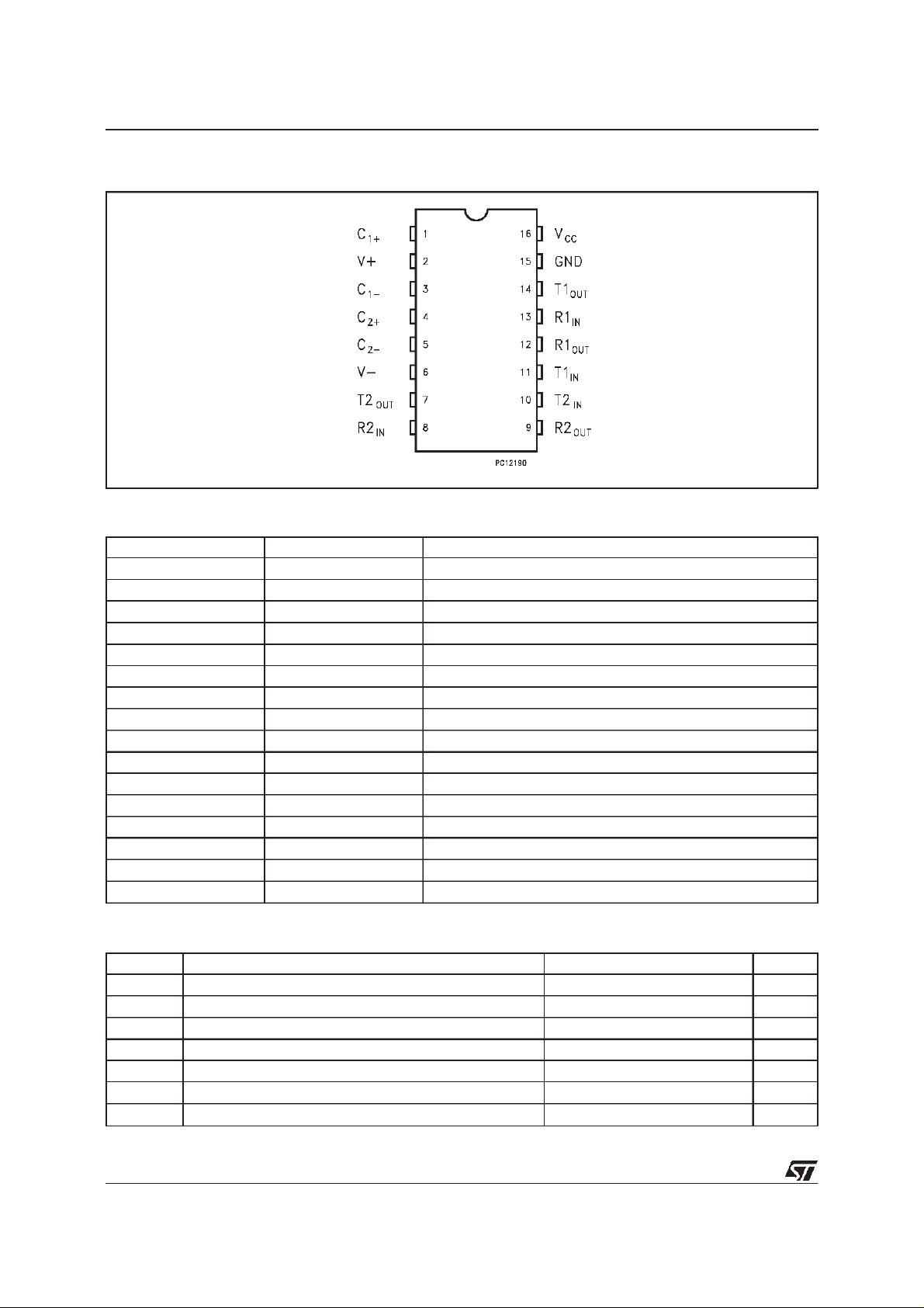
PIN CONFIGURATION
PIN DESCRIPTION
PIN No SYMBOL NAME AND F UNCTION
1C
2 V+ Doubled Voltage Terminal
3C
4C
5C
6 V- Inverted Voltage Terminal
7T2
8R2
9R2
10 T2
11 T1
12 R1
13 R1
14 T1
15 GND Ground
16 V
+ Positive Terminal forthe first Charge Pump Capacitor
1
- Negative Terminal for the first Charge Pump Capacitor
1
+ Positive Terminal for the second Charge Pump Capacitor
2
- Negative Terminal for the second Charge Pump Capacitor
2
OUT
IN
OUT
IN
IN
OUT
IN
OUT
CC
Second Transmitter Output Voltage
Second Receiver Input Voltage
Second Receiver Output Voltage
Second Transmitter Input Voltage
First Transmitter Input Voltage
First Receiver Output Voltage
First Receiver Input Voltage
First Transmitter Output Voltage
Supply Voltage
ABSOLUTE MAXIMUM RATINGS(Note 1)
Symb o l Para met er Val u e Uni t
V
T
R
T
OUT
R
OUT
T
SCTOUT
T
AbsoluteMaximumRatingsarethosevaluesbeyond whichdamagetothedevicemayoccur.Functionaloperationunderthese condition isnotimplied.
Note1:Noexternalsupply canbeappliedtoV+terminalandV- terminal.
2/11
Supply Voltage -0.3 to 6 V
CC
Transmitter Input Voltage Range -0.3 to (VCC+ 0.3) V
IN
Receiver Input Voltage Range ±30 V
IN
Transmitter Output Voltage Range (V+ + 0.3) to (V- - 0.3) V
Receiver Output Voltage Range -0.3 to (VCC+ 0.3) V
Short Circuit Duration on T
Storage Temperature Range -65 to +150
stg
OUT
infinite
o
C

ST232
ELECTRICAL CHARACTERISTICS
(C
TypicalValus are referred to T
Symbol Parameter Test Conditions Value Unit
TRANSMITTERELECTRICAL CHARACTERISTICS
(C
TypicalValus are referred to T
Symbol Parameter Test Conditions Value Unit
Note1:Measuredfrom3Vto -3Vor from-3Vto3V.
Note2:One trasmitter output is loaded with R
= 0.1µF, VCC=5V±10% TA= -40 to 85oC, unless otherwisespecified.
1-C4
=25oC)
A
I
SUPPLYVCC
1-C4
V
TOUT
Power Supply Current No Load, TA=25oC 5 10 mA
= 0.1µF, VCC=5V±10%, TA= -40 to 85oC, unless otherwise specified.
=25oC)
A
Output Voltage Swing All Transmitter outputs are
loaded with 3KΩto GND
Logic Pull-Up Current TIN= 0 V 15 200
I
TIL
Input Logic Threshold Low 0.8 V
V
TIL
V
SR
R
Input Logic Threshold High 2 V
TIH
Transition Slew Rate TA=25oC, VCC=5V,
T
D
Data Rate (Note 2) 120 220 Kbits/s
R
Transmitter Output Resistance VCC= V+ = V- = 0V
TOUT
Transmitter Output Short Circuit
I
SC
=3to7KΩ,
R
L
= 50 to 2500 pF (Note 1)
C
L
=±2V
V
OUT
one T
to GND ±10 ±60 mA
XOUT
Current
=3KΩto7KΩ,CL= 50 to 1000pF
L
Min. Typ. Max.
Min. Typ. Max.
±5 ±7.8 V
µ
730V/
300 Ω
A
s
µ
RECEIVERELECTRICAL CHARACTERISTICS
(C
TypicalValus are referred to T
Symbol Parameter Test Conditions Value Unit
Note1:RS-232INtoTTL-CMOSOUT(from50% to50%)
= 0.1µF, VCC=5V±10%, TA= -40 to 85oC, unless otherwise specified.
1-C4
=25oC)
A
V
Receiver Input Voltage Operating
RIN
Range
R
V
V
V
V
V
I
RS-232 Input Resistance TA=25oC, VCC=5V,
RIN
RS-232 Input Logic Threshold Low TA=25oC, VCC= 5 V 0.8 1.2 V
RIL
RS-232 Input Logic Threshold High TA=25oC, VCC= 5 V 1.7 2.4 V
RIH
RS-232 Input Hysteresis VCC= 5 V 0.2 0.5 1 V
RIHYS
TTL/CMOS Output Voltage Low I
ROL
TTL/CMOS Output Voltage High I
ROH
Propagation Delay Time CL=150pF (Note 1) 0.3 1
t
dR
Receiver Output Short Circuit Current
SCR
=5V
V
RIN
= 3.2mA (to VCC) 0.4 V
OUT
= 1mA (to GND) 3.5 VCC-0.4 V
OUT
Min. Typ. Max.
-30 30 V
357K
µ
10 mA
±
Ω
s
3/11
ST232
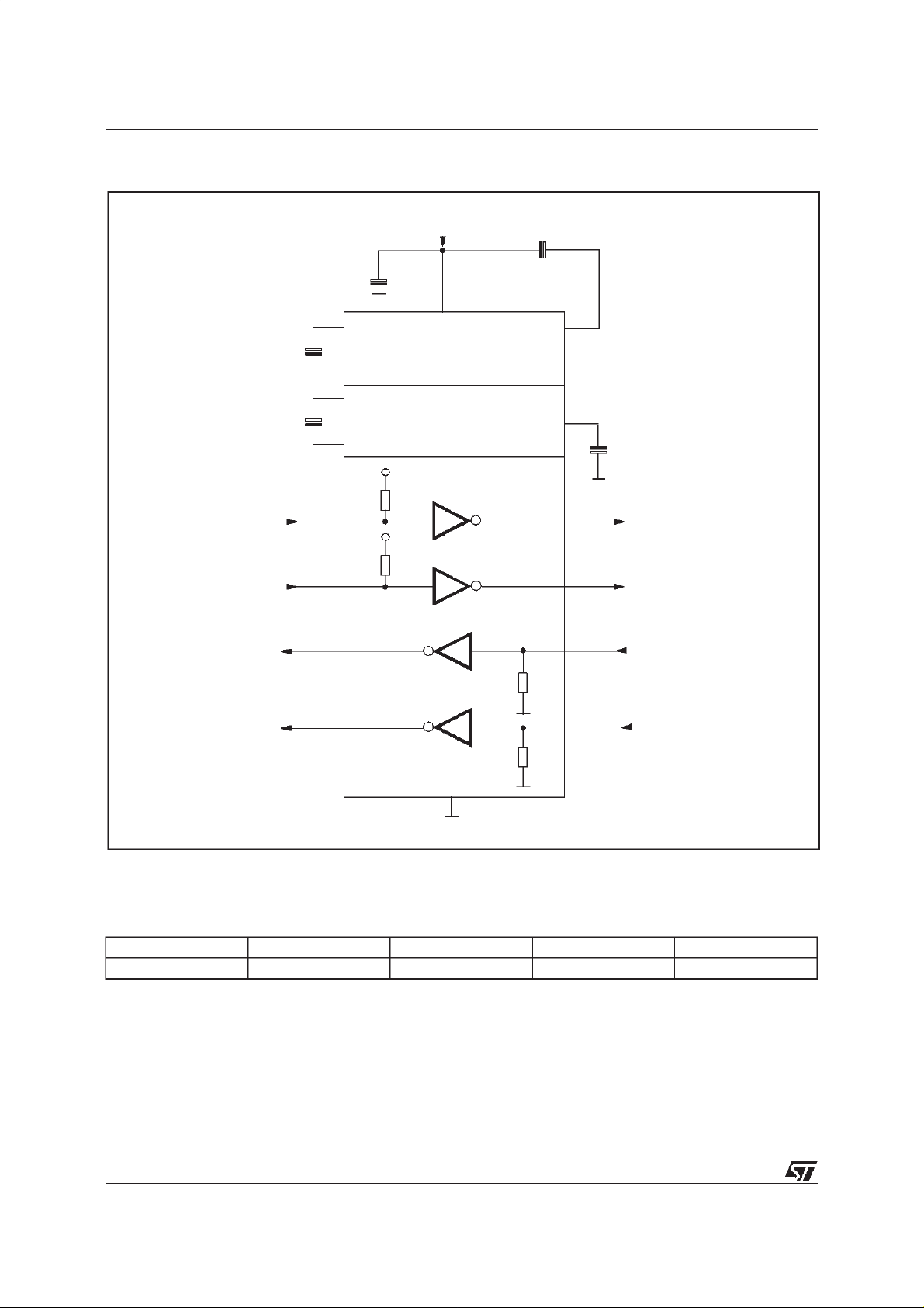
APPLICATION CIRCUITS
TTL / CMOS INPUTS
(note 1, note 2)
C5
1
C1+
+
C1
3
C1-
4
C2+
+
C2
C2-
5
11
IN
10
T2
IN
+5V INPUT
+
+5VTO +10V
VOLTAGE
DOUBLER
+10VTO -10V
VOLTAGE
INVERTER
+5V
400K
+5V
400K
16
Vcc
T1
T2
C3
T1
T2
V+
V-
OUTT1
OUT
+
2
+10V
6
-10V
C4
+
14
RS 232OUTPUTS
7
TTL / CMOS OUTPUTS
Note1:C
Note2:C
capacitorscanevenbe 1 µFones.
1-4
canbecommonor biasedcapacitors.
1-4
CapacitanceValue (µF)
C1 C2 C3 C4 C5
0.1 0.1 0.1 0.1 0.1
12
9
OUT
R1
R2OUT
R1
R2
GND
15
R1IN
5K
R2
5K
13
RS 232INPUTS
IN
8
4/11
 Loading...