


FEATURES
■ Application specific features
• 12 channel GPS correlation DSP hardware,
ST20 CPU (for control and position
calculations) and memory on one chip
• no TCXO required
• RTCA-SC159 / WAAS / EGNOS supported
■ GPS performance
• accuracy
- stand alone withSA on <100m, SA off <30m
- differential <1m
- surveying <1cm
• time to first fix
- autonomous start 90s
- cold start 45s
- warm start 7s
- obscuration 1s
■ Enhanced 32-bit VL-RISC CPU - C2 core
• 16/33/50 MHz processor clock
• 25 MIPS at 33 MHz
• fast integer/bit operations
■ 64 Kbytes on-chip SRAM
■ 128 Kbytes on-chip ROM
■ Programmable memory interface
• 4 separately configurable regions
• 8/16-bits wide
• support for mixed memory
• 2 cycle external access
■ Programmable UART (ASC)
■ Parallel I/O
■ Vectored interrupt subsystem
■ Diagnostic control unit
■ Power management
• low power operation
• power down modes
■ Professional toolset support
• ANSI C compiler/link driver and libraries
• Debugging/profiling and simulation tools
■ Technology
• Static clocked 50 MHz design
• 3.3 V, sub micron technology
■ 100 pin PQFP package
■ JTAG Test Access Port
ST20-GP6
GPS PROCESSOR
PRELIMINARY DATA
GPS
radio
ST20-GP6
12 channel GPS
hardware DSP
Low
power
controller
Real time
clock/calendar
Programmable
memory
interface
64K
SRAM
128K optional
mask ROM
APPLICATIONS
■ Global Positioning System (GPS) receivers
■ Car navigation systems
■ Fleet management systems
■ Time reference for telecom systems
ST20
CPU
Interrupt
controller
Serial
communications
2 UART (ASC)
Parallel
input/output
Diagnostic
control unit
Test
access port
.
.
16
.
December 1998
The information in this datasheet is subject to change
42 1707 02
1/123

ST20-GP6
Contents
1 Introduction . . . . . . . . . . . . ................................................ 5
2 ST20-GP6 architecture overview . . . . . ...................................... 7
3 Digital signal processing module . . . . . . . . . . . . . . . . .......................... 11
3.1 DSP module registers ........................................................................................................................... 13
4 Central processing unit . . . . . . . . . . . . . ..................................... 19
4.1 Registers ............................................................................................................................................... 19
4.2 Processes and concurrency ................................................................................................................. 20
4.3 Priority ................................................................................................................................................... 22
4.4 Process communications ...................................................................................................................... 23
4.5 Timers ................................................................................................................................................... 23
4.6 Traps and exceptions ........................................................................................................................... 24
5 Interrupt controller . . . . . . . . . . . . . . . . . . . . . . . . . . . . . . . . . . . . . . . . . . . . . . . . . . . . . . 30
5.1 Interrupt vector table ............................................................................................................................. 31
5.2 Interrupt handlers .................................................................................................................................. 31
5.3 Interrupt latency .................................................................................................................................... 32
5.4 Preemption and interrupt priority .......................................................................................................... 32
5.5 Restrictions on interrupt handlers ......................................................................................................... 33
5.6 Interrupt configuration registers ............................................................................................................ 33
6 Interrupt level controller . . . . . . . . . . . . . . . . . . . . . . . . . . . . . . . . . . . . . . . . . . . . . . . . . . 37
6.1 Interrupt assignments ........................................................................................................................... 37
6.2 Interrupt level controller registers ......................................................................................................... 37
7 Instruction set . . . . . . . . . . . . . . . . . . . . . . . . . . . . . . . . . . . . . . . . . . . . . . . . . . . . . . . . . . 40
7.1 Instruction cycles .................................................................................................................................. 40
7.2 Instruction characteristics ..................................................................................................................... 41
7.3 Instruction set tables ............................................................................................................................. 42
8 Memory map . . . . . . . . . . . . . . . . . . . . . . . . . . . . . . . . . . . . . . . . . . . . . . . ............ 51
8.1 System memory use ............................................................................................................................. 51
8.2 Boot ROM ............................................................................................................................................. 52
8.3 Internal peripheral space ...................................................................................................................... 52
9 Memory subsystem . . . . . . . . . . . . . . . . . . . . . . . . . . . . . . . . . . . . . . . . . . . . . . . . . . . . . 55
9.1 SRAM ................................................................................................................................................... 55
9.2 ROM ..................................................................................................................................................... 55
2/123

ST20-GP6
10 Programmable memory interface . . . . . . . . . . . . . . . . . . . . . . . . . . . . . . . . . . . . . . . . . . 56
10.1 EMI signal descriptions ......................................................................................................................... 58
10.2 External accesses ................................................................................................................................. 59
10.3 MemWait ............................................................................................................................................... 60
10.4 EMI configuration registers ................................................................................................................... 62
10.5 Boot source ........................................................................................................................................... 65
10.6 Default configuration ............................................................................................................................. 65
11 Low power controller . . . . . . . . ............................................ 66
11.1 Low power control ................................................................................................................................. 66
11.2 Low power configuration registers ........................................................................................................ 67
12 Real time clock and watchdog timer . . . . . . . . . ............................... 70
12.1 Power supplies ..................................................................................................................................... 70
12.2 Real time clock ..................................................................................................................................... 70
12.3 Watchdog timer ..................................................................................................................................... 70
12.4 RTC/WDT configuration registers ......................................................................................................... 71
13 System services . . . . . . . . . . . . . . . . . . . . . . . . . . . . . . . . . . . . . . . ................. 73
13.1 Reset, initialization and debug .............................................................................................................. 73
13.2 Bootstrap .............................................................................................................................................. 73
13.3 Clocks ................................................................................................................................................... 73
14 Diagnostic controller . . . . . . . . . . . . . . . . . . . . . . . . . . . . . . . . . . . . . . . . . . . . . . . . . . . . 75
14.1 Diagnostic hardware ............................................................................................................................. 75
14.2 Access features .................................................................................................................................... 76
14.3 Software debugging features ................................................................................................................ 77
14.4 Controlling the diagnostic controller ...................................................................................................... 79
14.5 Peeking and poking the host from the target ........................................................................................80
14.6 Abortable instructions ........................................................................................................................... 80
15 UART interface (ASC) . . . . . . . . . . . . . . . . . . . . . . . . . . . . . . . . . . . . . . . . . . . . . . . . . . . . 82
15.1 Functionality .......................................................................................................................................... 82
15.2 Timeout mechanism ............................................................................................................................. 85
15.3 Baud rate generation ............................................................................................................................ 85
15.4 Interrupt control .................................................................................................................................... 86
15.5 ASC configuration registers .................................................................................................................. 88
16 Parallel input/output . . . . . . . . . . . . . . . . . . . . . . . . . . . . . . . . . . . . . . . . . . . . . ........ 94
16.1 PIO Ports0-1 ......................................................................................................................................... 94
17 Configuration register addresses . . . . . . . . . . . . . . . . . . . . . . . . . . . . . . . . . . . . . . . . . . 96
3/123

ST20-GP6
18 Electrical specifications . . . . . . . . . . . . . . . . . . . . . . . . . . . . . . . . . . . . . . . . . . . . . . . . . . 102
19 GPS Performance . . . . . . . . . . . . . . . . . . . . . . . . . . . . . . . . . . . . . . . . ...............106
19.1 Accuracy ............................................................................................................................................... 106
19.2 Time to first fix ...................................................................................................................................... 107
20 Timing specifications . . . . . . . . . . . . . . . . . . . . . . . . . . . . . . . . . . . . . . . .............108
20.1 EMI timings ........................................................................................................................................... 108
20.2 Reset timings ........................................................................................................................................ 110
20.3 PIO timings ........................................................................................................................................... 111
20.4 ClockIn timings ..................................................................................................................................... 112
20.5 JTAG IEEE 1149.1 timings ................................................................................................................... 113
21 Pin list . . . . . . . . . . . . . . . . . . . . . . . . . . . . . . . . . . . . . . . . . . . . . . . . . . . . . . . . . . . . . . . . 114
22 Package specifications . . . . . . . . . . . . . . . . . . . . . . . . . .........................116
22.1 ST20-GP6 package pinout ................................................................................................................... 116
22.2 100 pin PQFP package dimensions ..................................................................................................... 119
23 Test access port . . . . . . . . . . . . . . . . . . . . . . . . . . . . . . . . . . . . . . . . . . . . . . . . . . . . . . . . 121
24 Device ID . . . . . . . . . . . . . . . . . . . . . . . . . . . . . . . . . . . . ..........................122
25 Ordering information . . . . . . . . ............................................122
4/123

ST20-GP6
1 Introduction
The ST20-GP6 is an application-specific single chip micro using the ST20 CPU with
microprocessor style peripherals added on-chip. It incorporates DSP hardware for processing the
signals from GPS (Global PositioningSystem) satellites.
The twelve channel GPS correlation DSP hardware is designed to handle twelve satellites, two of
which can be initialized to support the RTCA-SC159 specification for WAAS (Wide Area
Augmentation Service) and EGNOS (European Geostationary Navigation Overlay System)
services.
The ST20-GP6 has been designed to minimize system costs and reduce the complexity of GPS
systems. It offers all hardware DSP and microprocessor functions on one chip and provides
sufficient on-chip RAM and ROM. The entire analogue section, RF and clock generation are
availableon a companion chip.Thus, a complete GPS system is possible using just two chips, see
Figure 1.1.
Antenna
STB5600
Radio
Single chip
Low
cost
crystal
No TCXO
ST20-GP6
DSP
ASIC
optional
mask ROM
CPU
Watchdog
timer
RAM
UART
Parallel
I/O
Real
time
clock
Driver
(optional)
Parallel I/O
Figure 1.1 GPS system
The ST20-GP6 supports large values of frequency offset, allowing the use of a very low cost
oscillator,thus saving the cost of a TemperatureControlled Crystal Oscillator (TCXO).
The CPU and software have access to the part-processed signal to enable accelerated acquisition
time.
5/123

ST20-GP6
The ST20-GP6 can implement the GPS digital signal processing algorithms using less than 50% of
the available CPU processing power.This leaves the rest availablefor integrating OEM application
functions such as route-finding, map display and telemetry. A hardware microkernel in the ST20
CPU supports the sharing of CPU time between tasks without an operating system or executive
overhead.
The architecture is based on the ST20 CPU core and supporting macrocells developed by
STMicroelectronics. The ST20 micro-core family provides the tools and building blocks to enable
the development of highly integrated application specific 32-bit devices at the lowest cost and
fastest time to market. The ST20 macrocell library includes the ST20Cx family of 32-bit VL-RISC
(variable length reduced instruction set computer) micro-cores, embedded memories, standard
peripherals, I/O, controllers and ASICs.
The ST20-GP6 uses the ST20 macrocell library to provide the hardware modules required in a
GPS system. These include:
• DSP hardware
• Dual channel UART for serial communications
• Two parallel I/O modules providing 16 bits of parallel I/O
• Interrupt controller
• Real time clock/calendarand watchdog timer
• 128 Kbytes of on-chip ROM for application code
• 64 Kbytesof on-chip RAM, of which 16 Kbytes is battery backed
• Diagnostic control unit and test access port for development support
The ST20-GP6 is supported by a range of software and hardware development tools for PC and
UNIX hosts including an ANSI-C ST20 software toolset and the ST20 INQUEST window based
debugging toolkit.
6/123

ST20-GP6
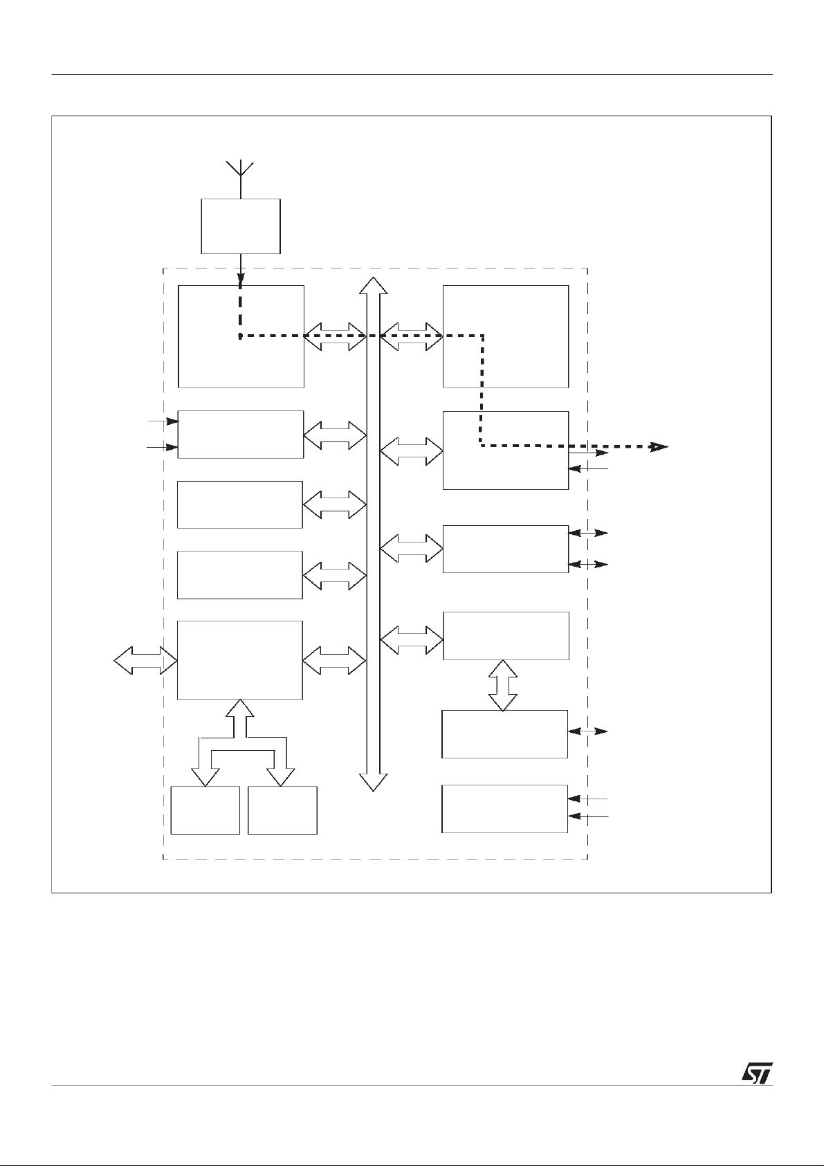
2 ST20-GP6 architecture overview
The ST20-GP6 consists of an ST20 CPU plus application specific DSP hardware for handling GPS
signals, plus a dual channel UART, ROM and RAM memory, parallel IO, real time clock and
watchdog functions.
Figure 2.1 shows the subsystem modules that comprise the ST20-GP6. These modules are
outlined below and more detailed information is given in the followingchapters.
DSP
The ST20-GP6 includes DSP hardware for processing signals from the GPS satellites. The DSP
module generates the pseudo-random noise (prn) signals, and de-spreads the incoming signal.
It consists of a down conversion stage that takes the 4 MHz input signal down to nominally zero
frequency both in-phase and quadrature (I & Q). This is followed by 12 parallel hardware channels
for satellite tracking, whose output is passed to the CPU for further software processing at a
programmableinterval, nominally every millisecond.
CPU
The Central Processing Unit (CPU) on the ST20-GP6 is the ST20 32-bit processor core. It contains
instruction processing logic, instruction and data pointers, and an operand register. It directly
accesses the high speed on-chip memory, which can store data or programs.The processor can
access up to 4 Mbytes of memory via the programmablememory interface.
7/123
ST20-GP6
GPS
radio
ST20-GP6
Interrupts
12 channel GPS
hardware DSP
Interrupt
controller
Low
power
controller
Real time
clock
Programmable
memory
interface
ST20
CPU
Serial
communications
2 UART
Parallel
input/output
Diagnostic
control unit
Test access
port
User position
output in
ASCII
.
.
16
.
128K
ROM
64K
SRAM
System
services
Reset
Clock
Figure 2.1 ST20-GP6 architectural block diagram
Memory subsystem
The ST20-GP6 on-chip memory system provides 60 Mbytes/s internal data bandwidth, supporting
pipelined 2-cycle internal memory access at 30 ns cycle times. The ST20-GP6 memory system
consists of SRAM, ROMand a programmableexternal memory interface (EMI).
8/123

ST20-GP6
The ST20-GP6 can use 8 or 16-bit external RAM, 8 or 16-bit external ROM, and has a 20-bit
address bus.
The ST20-GP6 product has 64 Kbytes of on-chip SRAM. This is in 4 banks of 16 Kbytes. One of
these banks is powered from the back-up battery supply.The ST20-GP6 has 128 Kbytes of ROM
for application code.
The ST20-GP6 memory interface controls the movement of data between the ST20-GP6 and offchip memory.It is designed to support memory subsystems without any external support logic and
is programmableto support a wide range of memory types. Memory is divided into 4 banks which
can each have different memory characteristics and each bank can access up to 1 Mbyte of
external memory.
The normal memory provision in a simple GPS receiver is a single 64K x 16-bit ROM or Flash
ROM (70, 90 or 100 ns access time). The internal 64 Kbyte RAM is sufficient for application use,
howeverfor development purposes external RAM may be added. The ST20-GP6 can supportup to
1 Mbyte of SRAM plus 1 Mbyte of ROM, enabling additional functions to be added if required.
Low power controller, real time clock and watchdog timer
The ST20-GP6 has power-down capabilities configurable in software. When powered down, a
timer can be used as an alarm, re-activating the CPU after a programmed delay.This is suitable for
ultra low power or solar powered applications such as container tracking, railway truck tracking, or
marine navigation buoysthat must checkthey are on station at intervals.
There is also a watchdog timer (WDT), resetting the system if it times out. The watchdog timer
function is enabled by an external pin (WdEnable). The WDT has a counter, clocked to give a
nominal 2 second delay.A status flag (notWdReset) is set by a watchdog reset. This can be used
to indicate to application code that the system wasreset by the watchdog timer.
The real time clock (RTC) provides a set of continuously running counters to provide a clockcalendar function. The counter values can be written to set the current time/data. The RTC is
clockedbya 32,768 Hz crystal oscillator and has a separate powersupply so that it cancontinue to
run when the rest of the chip is powereddown.
The RTC contains two counters: a 30-bit ‘milliseconds’ counter and a 16-bit ‘weeks’ counter. This
allows large time values to be represented to high accuracy. Note that the milliseconds counter is
actually clockedat 1.024 KHz and this must be handled by software.
The ST20-GP6 is designed for 0.35 micron, 3.3 V CMOS technology and runs at speeds of up to
50 MHz. 3.3 V operation provides reduced power consumption internally and allows the use of low
power peripherals. In addition, a power-down mode is available on the ST20-GP6.
The different power levels of the ST20-GP6 are listed below.
• Operating power — power consumed during functional operation.
• Stand-bypower — power consumed during little or no activity. The CPU is idle but ready to
immediately respond to an interrupt/reschedule.
• Power-down — clocks are stopped and power consumption is significantly reduced. Functional operation is stalled. Normal functional operation can be resumed from previous state
as soon as the clocks are stable. No information is lost during power down as all internal
logic is static.
9/123

ST20-GP6
• Power to most of the chip removed— only the real time clock supply (RTCVDD) power on.
In power-downmode the processor and all peripherals are stopped, including the external memory
controller and optionally the PLL. Effectively the internal clock is stopped and functional operation
is stalled. On restart the clock is restarted and the chip resumes normal functional operation.
Serial communications
The ST20-GP6 has two UARTs (Asynchronous Serial Controllers (ASCs)) for serial
communication. The UARTs provide an asynchronous serial interface and can be programmed to
support a range of baud rates and data formats,for example,data size, stop bits and parity.
Interrupt subsystem
The ST20-GP6 interrupt subsystem supports eight prioritized interrupts. Four interrupts are
connected to on-chip peripherals (2 for the UARTs, 2 for the programmable IO), two are available
as external interrupt pins and two are spare.
Each interrupt level has a higher priority than the previous and each level supports only one
software handler process.
Note that interrupt handlers must not prevent the GPS DSP data traffic from being handled. During
continuous operation this has 1 ms latency and is not a problem, but during initial acquisition it has
a32µs rate and thus all interrupts must be disabledexcept if used to stop GPS operation.
Parallel IO module
Sixteen bits of parallel IO are provided. Each bit is programmableas an output or an input. Edge
detection logic is provided which can generate an interrupt on any change of an input bit.
JTAGTest Access Port
The Test Access Port (TAP) supports the IEEE 1149.1 JTAG test standard.
Diagnostic controller
The diagnostic controller is a programmablemodule which connects directly into the CPU.It can be
accessed by the TAP. This allows debugging systems to be used which do not affect CPU
performance or intrude into application code. Debugging support includes:
• hardware breakpoint and watchpoint
• real time trace
• external LSA triggering support
It is also used to provide system services, including booting the CPU.
System services module
The ST20-GP6 system services module includes:
• reset and initialization port.
• phase locked loop (PLL) — accepts 16.368 MHz input and generates all the internal high
frequency clocks needed for the CPU.
10/123
ST20-GP6
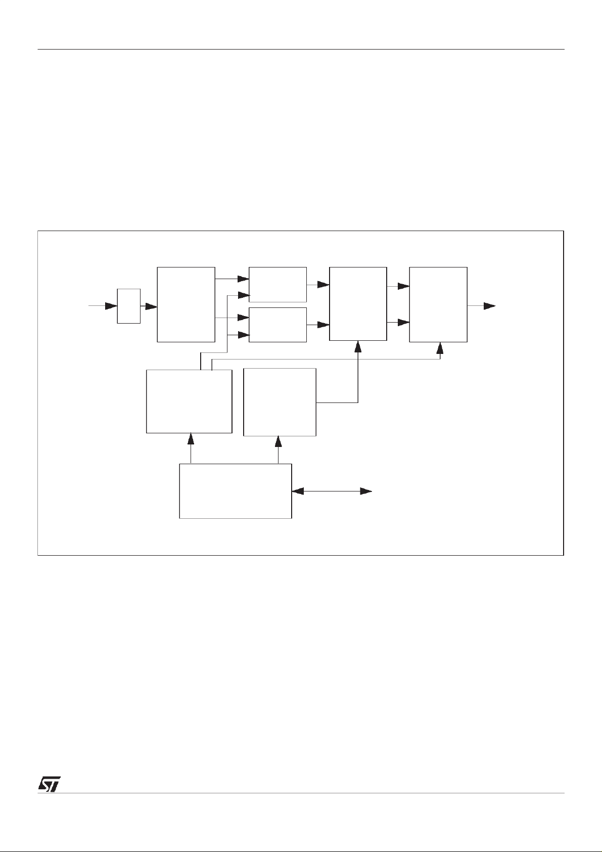
3 Digital signal processing module
The ST20-GP6 chip includes 12 channel GPS correlation DSP hardware. It is designed to handle
twelve satellites, two of which can be initialized to support the RTCA-SC159specification.
The digital signal processing (DSP) module extracts GPS data from the incoming IF (Intermediate
Frequency) data. There are a number of stages of processing involved; these are summarized
below and in Figure 3.1. After the 12 pairs of hardware correlators, the data for all channels are
time division multiplexed onto the appropriate internal buses (i.e. values for each channel are
passed in sequence, for example: I1,Q1,I2,Q2... I12,Q12,I1,Q1).
4 MHz IF
input
data
sampler
frequency
converter A
Pseudo random
noise sequence
generator
(x 12)
ST20 CPU accessible
registers
I correlator
(x 12)
Q correlator
(x 12)
Numerically
controlled
oscillator
frequency
converter B
DMA
interface
accumulator
Figure 3.1 DSP module blockdiagram
The main stages of processing are as follows:
Data sampling
This stage removes any meta-stability caused by the asynchronous input data coming from an
analogue source (the radio receiver). The data at this point consists of a carrier of nominally
4.092 MHz with a bandwidth of approximately±1 MHz.
This stage is common to all 12 channels.
11/123

ST20-GP6
Frequency conversion (A)
The first frequency converter mixes the sampled IF data with the (nominal) 4.092 MHz signal. This
is done twice with a quarter cycle offset to produce I and Q (In-phase and Quadrature) versions of
the data at nominal zero centre frequency (this can actually be up to ±132 KHz due to errors such
as doppler shift, crystal accuracy,etc.). The sum frequency (~8 MHz) is removedby low-pass filtering in the correlator.
This stage is common to all 12 channels.
Correlation against pseudo-random sequence
The GPS data is transmitted as a spread-spectrum signal (with a bandwidth of about 2 MHz). In
order to recover the data it is necessary to correlate against the same Pseudo-Random Noise
(PRN) signal that was used to transmit the data. The output of the correlator accumulator is sampled at 264 KHz. The PRN sequences come from the PRN generator.
There is a correlator for the I and Q signals for each of the 12 channels. The output signal is now
narrowband.
Frequency conversion (B)
The second stage of frequency conversion mixes the data with the local oscillator signal generated
bythe Numerically Controlled Oscillator (NCO). This signal is locked, under software control, to the
Space Vehicle (SV) frequency and phase to remove the errors and take the frequency and bandwidth of the data down to 0 and ±50 Hz respectively.Filtering to 500 Hz is achievedin hardware,to
50 Hz in software.
This stage is shared by time division multiplexing between all 12 channels. This is loss-free as the
stage supports 12 channels x 264 KHz, approximately 3 MHz, well within its 16 MHz clock rate.
Result integration
The final stage sums the I and Q values for each channel over a user defined period. In normal
operation, the sampling period is slightly less than the 1ms length of the PRN sequence. This
ensures that no data is lost, although it may mean that some data samples are seen twice — this is
handled (mainly) in software.
The sampling period can also be programmed to be much shorter (i.e. a higher cut-off frequency
for the filter) when the system is trying to find new satellites (‘acquisition mode’).
There are two further stages of buffering for the accumulated 16-bit I and Q values for each channel. These allow for the slightly differenttime domains involved1.
The results after hardware processing of the signal, using the parameters set in the DSP registers,
refer to Section 3.1, are delivered to the CPU via a DMA engine in packet format. The CPU should
perform an
in
(input) instruction on the appropriate channel (see address map, Figure 8.1 on
page 53) in order to read a packet.
The format of the 62-byte packets is given in Figure 3.2. These represent a two byte header, fol-
lowedby the 16-bit I-valuesfor 12 channels, then the 16-bit Q-values for 12 channels, then the 8-bit
timestamp values for the 12 channels. The I and Q values are sent least significantbyte first. The 2
1. Data sampled in SV time, data transmitted to the CPU at fixedintervals.
12/123

ST20-GP6
byte header contains: a ‘sync’ byte with the value #1B, and a ‘sample rate’ byte which contains the
two SampleRate bits from the DSPControl register,see Table3.1.
Packetsare delivered at the rate selected by the DSPControl register, evenif new data is not available. In this case, the data value for the field is set to #8000. This guarantees that synchronism is
maintained between the satellite one-millisecond epochs and the receiver, despite time-of-reception variations due to the varying path length from the satellite.
62 byte packet every 840/970/31/62 µs
16-bit
header
sync
12 x 16-bit
I values
sample
rate
12 x 16-bit
Q values
Absent 16-bit values padded with #8000
Trackingmode
T[7:6] = 10
T[5:0] = time[5:0]
Figure 3.2 DSP packet format
12 x 8-bit
time values
Acquisition mode
First packet (in SV ms)
T[7:6] = 10
T[5:0] = time[5:0]
Remaining packets
T[7:6] = 00
T[5:0] = sequence number
(sequence numbers are 2 to
16 or 32)
3.1 DSP module registers
The GPS hardware channels of the ST20-GP6 are controlled bythree sets of registers:
1 DSPControl register
2 PRNcode0-11 and PRNphase0-11 registers
3 NCOfrequency0-11 and NCOphase0-11 registers
The base addresses for the DSP registers are given in the Memory Map chapter.
DSPControl register
The DSPControl register determineswhether the PRN generators are on (normal use) or disabled
(for built-in-self-test of a system), whether the system is in tracking mode (840/970 µs output rate)
or initial acquisition mode (31/62 µs), and selects which of the two rates for each mode. It also
13/123

ST20-GP6
determines whether the accumulated carrier phase in the NCO are reset to zero automatically or
continue from their existing value. The bit allocations are givenin Table3.1.
DSPControl DSP base address + #140 Write only
Bit Bit field Function
1:0 SampleRate These bits control the sampling rate (the rate at which data is sent to the DMA
controller). The encoding of these bits is as follows:
SampleRate[1:0] Transfer period
00 840 µs 256 Tracking
01 970 µs 256
10 31 µs 8 Acquisition
11 62 µs16
2NCOResetEnable When set to 1, the accumulated NCO phase for a channel is reset when the cor-
responding PRN code register is written.
3 PRNDisable When set to 1, all PRN generators are disabled.
No. of samples
accumulated
Mode
Table3.1 DSPControl register format
PRNcode0-11 registers
The PRNcode0-11 registers choose the code for the particular satellite, and writing these causes a
reset to the accumulated carrier phase in the NCO for the corresponding channel, if enabledby the
DSPControl register.
PRNcode0-11 DSP base address + #00 to #2C Write only
Bit Bit field Function
6:0 PRNcode Satellite code as a 7-bit value.
Table3.2 PRNcode0-11 register format
The bit-fields for selecting particular GPS satellites are given in Table3.3.
14/123

ST20-GP6
Satellite ID
1 #62 6 2
2 #73 7 3
3 #04 8 4
4 #15 9 5
5 #11 9 1
6 #22 10 2
7 #01 8 1
8 #12 9 2
9 #23 10 3
10 #32 3 2
11 #43 4 3
12 #65 6 5
13 #76 7 6
14 #07 8 7
15 #18 9 8
16 #29 10 9
17 #41 4 1
18 #52 5 2
19 #63 6 3
20 #74 7 4
21 #05 8 5
22 #16 9 6
23 #31 3 1
24 #64 6 4
25 #75 7 5
26 #06 8 6
27 #17 9 7
28 #28 10 8
29 #61 6 1
30 #72 7 2
31 #03 8 3
32 #14 9 4
- #25 10 5
- #24 10 4
- #71 7 1
- #02 8 2
- #24 10 4
b
WAAS
PRNcode0-11
register value
#20 10 0
Taps selected from G2 shift register
by bits 6 to 4 by bits 3 to 0
a
Table 3.3 PRNcode0-11 register value
a. Refer to the US DoD document ICD-GPS-200.
b. It is the responsibility of the software to ensure that when this value is selected, a suitable
value has been written into the PRNinitialVal0-1 register. If this channel is later used fora
standard GPS satellite, the PRNinitialVal0-1 must be set to all ones (#3FF).
For channels 0 and 1, RTCA-SC159 satellite codes can also be selected. This is achieved by setting the PRNcode0-11 register appropriately and also writing the initial value for the satellite to the
15/123

ST20-GP6
PRNinitialVal0-1 register, see Table3.8. If uninitialized by the software, the PRNinitialVal register
defaults to 11 1111 1111 (#3FF) as required for GPS satellites.
The PRNcode0-11 and PRNinitialVal0-1 registers are normally written only when the satellite is
first chosen.
PRNphase0-11 registers
The PRN0-11phase registers determine the relativedelay between the receiver master clock, and
the start of the one millisecond repetitive code sequence. The code sequence starts when the
receiver clock counter (invisible to the software except through message timestamps) reaches the
value written to the PRNphase0-11 register. The PRNphase0-11 register must only be written
once per satellite milliseconds-epoch, which varies from the receiver epoch dynamically due to satellite motion. Synchronism with the software is achieved by reading the register, when a write
enable flag is returned. If not enabled, the write operation is abandoned by the software.
The 19-bit valuecomprises three fields.The 3 least significant bits represent the fractional-delay in
eighths of a code-chip. The middle 10 bits represent the integer delay in code-chips, 0-1022, with
the value 1023 illegal. The upper 6 most significant bits represent the delay in integer milliseconds.
PRNphase0-11 DSP base address + #40 to #6C Write only
Bit Bit field Function
2:0 FractionalDelay Fractional delay in eighths of a code-chip.
12:3 IntegerDelay Integer delay in code-chips. Value 0-1022. Note, the value 1023 is illegal.
18:13 Delay Delay in integer milliseconds.
Table 3.4 PRNphase0-11 register format
Note also that the eighth-chip resolution of the code generator is not sufficient for positioning. At
125 ns it represents approximately40 m of range,over 100 m of position. The software must maintain the range measurements around the 1 ns resolution level in a 32-bit field, and send an appropriate 19-bit sub-field to the register. Note, care must be taken when calculating this field from a
computed delay,or vice versa,to allow forthe missing value1023. The overallregister bit-field cannot be used mathematically as a single binary number.
PRNphase0-11WrEn registers
The PRNphase0-11WrEn flags are active low flags that record when the PRNphase0-11 register
can be updated. The PRNphaseWrEn flag for a channel is set high when the corresponding PRN-
phase register is written. The flag is reset again when the value written is loaded into the PRN gen-
16/123

ST20-GP6
erator. Note, the PRNphase0-11 register should only be updated when the PRNphase0-11WrEn
register has been cleared by the hardware.
PRNphase0-11WrEn DSP base address + #40 to #6C Read only
Bit Bit field Function
0 PRNphaseWrEn
Set when the corresponding PRNphase0-11 register is set.
Table3.5 PRNphase0-11WrEn register format
NCOfrequency0-11 registers
The NCOfrequency0-11 registers hold a signed 18-bit value that is added repetitively, ignoring
overflows, to the accumulated NCO phase from which the NCO sine and cosine waveforms are
generated. The addition is performed at a 264 KHz rate (16.368MHz/62). The accumulated NCO
phase is not accessible to the software, but can be cleared when initialising the channel if enabled
by the DSPControl register.
Each unit value in the NCOfrequency0-11 register represents 264KHz/(218), i.e.
1.007080078125 Hz.
If the extreme values are written, #1FFFF and #20000, the sine wave generated will be at approxi-
mately +132 KHz, and precisely -132 KHz respectively.
NCOfrequency0-11 DSP base address + #80 to #AC Write only
Bit Bit field Function
17:0 NCOfrequency NCO frequency as a signed 18-bit value.
Table 3.6 NCOfrequency0-11 register format
NCOphase0-11 registers
The NCOphase0-11 registers contents are added to the accumulated phase to correct the carrier
for the final 1 Hz that cannot be resolved by the NCO frequency.This addition is not cumulative,
and the value must be updated regularly by the software as a result of carrier phase errors measured on the satellite signal. The register holds a signed 7-bit field representing +/-180 degrees
total in steps of 2.8125 degrees(360/128).
NCOphase0-11 DSP base address + #C4 to #EC Write only
Bit Bit field Function
6:0 NCOphase NCO phase as a signed 7-bit value representing +/-180 degrees total in steps of
2.8125 degrees (360/128).
Table 3.7 NCOphase0-11 register format
17/123

ST20-GP6
PRNinitialVal0-1 registers
The initial value for the two RTCA-SC159 capable satellites channels should be written to the
PRNinitialVal0-1 registers. The value can be foundin the
RTCA-SC159 Specification
.
Note: The value written to the register is the Initial Value defined by RTCA-SC159 for the PRN
required. The conversion from ‘big-endian’ as used in the specification to ‘little-endian’ as conventionally used in ST20 architectures has been implemented in the hardware.
If uninitialized by the software, this register defaults to 11 1111 1111 (#3FF) as required for GPS
satellites.
PRNinitialVal0-1 DSP base address + #100, #104 Write only
Bit Bit field Function
9:0 InitialValue Initial value of the RTCA-SC159 satellite channel.
Table 3.8 PRNinitialVal0-1 register format
18/123

ST20-GP6
4 Central processing unit
The Central Processing Unit (CPU) is the ST20 32-bit processor core. It contains instruction processing logic,instruction and data pointers, and an operand register. It can directly access the high
speed on-chip memory, which can store data or programs. Where larger amounts of memory are
required, the processor can access memory via the External Memory Interface (EMI).
The processor provides high performance:
• Fast integer multiply - 4 cycle multiply
• Fast bit shift - single cycle barrel shifter
• Byte and part-wordhandling
• Scheduling and interrupt support
• 64-bit integer arithmetic support.
The scheduler provides a single level of pre-emption. In addition, multi-level pre-emption is provided by the interrupt subsystem, see Chapter 5 for details. Additionally, there is a per-priority trap
handler to improvethe support for arithmetic errors and illegal instructions,refer to section 4.6.
4.1 Registers
The CPU contains six registers which are used in the execution of a sequential integer process.
The six registers are:
• The workspace pointer (Wptr) which points to an area of store where local data is kept.
• The instruction pointer (Iptr) which points to the next instruction to be executed.
• The status register (Status).
• The Areg, Breg and Creg registers which form an evaluationstack.
The Areg, Breg and Creg registers are the sources and destinations for most arithmetic and logical operations.Loading a value into the stack pushes Breg into Creg, and Areg into Breg, before
loading Areg. Storing a value from Areg, pops Breg into Areg and Creg into Breg. Creg is left
undefined.
Local data ProgramRegisters
Areg
Breg
Creg
Wptr
Iptr
Figure 4.1 Registers used in sequential integer processes
19/123

ST20-GP6
Expressions are evaluated on the evaluationstack, and instructions refer to the stack implicitly. For
example,the
the stack. The use of a stack removes the need for instructions to explicitly specify the location of
their operands. No hardware mechanism is provided to detect that more than three values have
been loaded onto the stack; it is easy for the compiler to ensure that this neverhappens.
Note that a location in memory can be accessed relative to the workspace pointer, enabling the
workspace to be of any size.
The use of shadow registers provides fast, simple and clean contextswitching.
add
instruction adds the top twovaluesin the stack and places the result on the top of
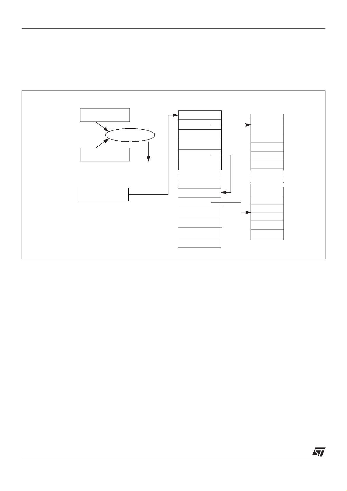
4.2 Processes and concurrency
The following section describes ‘default’ behavior of the CPU and it should be noted that the user
can alter this behavior,for example,by disabling timeslicing, installing a user scheduler,etc.
A process starts, performs a number of actions, and then either stops without completing or terminates complete. Typically, a process is a sequence of instructions. The CPU can run several processes in parallel (concurrently). Processes may be assigned either high or low priority, and there
maybe any number of each.
The processor has a microcoded scheduler which enables any number of concurrent processes to
be executed together, sharing the processor time. This removes the need for a software kernel,
although kernels can still be written if desired.
At any time, a process may be
active
inactive
The scheduler operates in such a way that inactive processes do not consume any processor time.
Each active high priority process executesuntil it becomes inactive.The scheduler allocates a portion of the processor’stime to each active low priority process in turn (see section 4.3). Active processes waiting to be executed are held in two linked lists of process work spaces, one of high
priority processes and one of low priority processes. Each list is implemented using two registers,
one of which points to the first process in the list, the other to the last. In the linked process list
shown in Figure 4.2, processSis executing andP,QandRare active, awaiting execution. Only the
low priority process queue registers are shown; the high priority process ones behavein a similar
manner.
- being executed,
- interrupted by a higher priority process,
- on a list waiting to be executed.
- waiting to input,
- waiting to output,
- waiting until a specifiedtime.
20/123

ST20-GP6
Registers
FptrReg1
BptrReg1
Areg
Breg
Creg
Wptr
Iptr
Local data
P
Q
R
S
Iptr.s
Link.s
Iptr.s
Link.s
Iptr.s
Program
Figure 4.2 Linked process list
Function High priority Low priority
Pointer to front of active process list
Pointer to back of active process list
FptrReg0 FptrReg1
BptrReg0 BptrReg1
Table4.1 Priority queue control registers
Each process runs until it has completed its action or is descheduled. In order for several processes to operate in parallel, a low priority process is only permitted to execute for a maximum of
two timeslice periods. After this, the machine deschedules the current process at the next timeslicing point, adds it to the end of the low priority scheduling list and instead executes the next active
process. The timeslice period is 1ms.
There are only certain instructions at which a process may be descheduled. These are known as
descheduling points. A process may only be timesliced at certain descheduling points. These are
known as timeslicing points and are defined in such a way that the operand stack is always empty.
This removes the need for saving the operand stack when timeslicing. As a result, an expression
evaluation can be guaranteed to executewithout the process being timesliced part waythrough.
Whenevera process is unableto proceed, its instruction pointer is savedin the process workspace
and the next process takenfrom the list.
The processor core provides a number of special instructions to supportthe process model, including
startp
struct,
(start process) and
startp
is used to create the necessary additional concurrent processes. A
endp
(end process). When a main process executes a parallel con-
startp
instruction
creates a new process by adding a new workspace to the end of the scheduling list, enabling the
new concurrent process to be executed together with the ones already being executed. When a
process is made active it is always added to the end of the list, and thus cannot pre-empt processes already on the same list.
The correct termination of a parallel construct is assured by use of the
endp
instruction. This uses
a data structure that includes a counter of the parallel construct components which have still to ter-
21/123

ST20-GP6
minate. The counter is initialized to the number of components before the processes are started.
Each component ends with an
the last component, the counter is non zero and the component is descheduled. For the last component, the counter is zero and the main process continues.
endp
instruction which decrements and tests the counter.Forall but
4.3 Priority
The following section describes ‘default’ behavior of the CPU and it should be noted that the user
can alter this behavior,for example,by disabling timeslicing and priority interrupts.
The processor can executeprocesses at one of two priority levels, one level for urgent (high priority) processes, one for less urgent (low priority) processes. A high priority process will alwaysexecute in preferenceto a low priority process if both are able to do so.
High priority processes are expected to execute for a short time. If one or more high priority processes are active, then the first on the queue is selected and executesuntil it has to wait for a communication, a timer input, or until it completes processing.
If no process at high priority is active, but one or more processes at low priority are active, then one
is selected. Low priority processes are periodically timesliced to provide an evendistribution of processor time between tasks which use a lot of computation.
If there arenlowpriority processes, then the maximum latency from the time at which a low priority
process becomes active to the time when it starts processing is the order of 2ntimeslice periods. It
is then able to execute for between one and two timeslice periods, less any time taken by high priority processes. This assumes that no process monopolizes the time of the CPU; i.e. it has frequent timeslicing points.
The specific condition for a high priority process to start executionis that the CPU is idle or running
at low priority and the high priority queue is non-empty.
If a high priority process becomes able to run while a low priority process is executing, the low priority process is temporarily stopped and the high priority process is executed. The state of the low
priority process is savedinto ‘shadow’ registers and the high priority process is executed.When no
further high priority processes are able to run, the state of the interrupted lowpriority process is reloaded from the shadow registers and the interrupted low priority process continues executing.
Instructions are provided on the processor core to allow a high priority process to store the shadow
registers to memory and to load them from memory. Instructions are also provided to allow a process to exchange an alternative process queue foreither priority process queue (see Table7.21 on
page 49). These instructions allow extensions to be made to the scheduler for custom run-time kernels.
A low priority process may be interrupted after it has completed execution of any instruction. In
addition, to minimize the time taken for an interrupting high priority process to start executing, the
potentially time consuming instructions are interruptible. Also some instructions may be aborted,
and are restarted when the process next becomes active (refer to the Instruction Set chapter).
22/123

ST20-GP6
4.4 Process communications
Communication between processes takes place over channels, and is implemented in hardware.
Communication is point-to-point, synchronized and unbuffered. As a result, a channel needs no
process queue, no message queue and no message buffer.
A channel between two processes executing on the same CPU is implemented by a single word in
memory; a channel between processes executingon differentprocessors is implemented by pointto-point links. The processor provides a number of operations to support message passing, the
most important beingin(input message) and
out
(output message).
Theinand
out
instructions use the address of the channel to determine whether the channel is
internal or external. This means that the same instruction sequence can be used for both hard and
soft channels, allowing a process to be written and compiled without knowledge of where its channels are implemented.
Communication takes place when both the inputting and outputting processes are ready. Consequently, the process which first becomes ready must wait until the second one is also ready. The
inputting and outputting processes only become activewhen the communication has completed.
A process performs an input or output by loading the evaluationstack with, a pointer to a message,
the address of a channel, and a count of the number of bytes to be transferred,and then executing
aninor
out
instruction.
4.5 Timers
There are two 32-bit hardware timer clocks which ‘tick’ periodically. These are independent of any
on-chip peripheral real time clock. The timers provide accurate process timing, allowing processes
to deschedule themselves until a specifictime.
One timer is accessible only to high priority processes and is incremented approximately every
microsecond, cycling completely in approximately 4295 seconds. The other is accessible only to
low priority processes and is incremented approximately every 64 microseconds, giving 15625
ticks per second. It has a full period of approximately 76 hours. Timer frequencies are approximate.
Register Function
ClockReg0 Current value of high priority (level 0) process clock.
ClockReg1 Current value of low priority (level1) process clock.
TnextReg0 Indicates time of earliest eventon high priority (level0) timer queue.
TnextReg1 Indicates time of earliest eventon low priority (level 1) timer queue.
TptrReg0 High priority timer queue.
TptrReg1 Low priority timer queue.
Table4.2 Timer registers
The current value of the processor clockcan be read by executinga
A process can arrange to perform a
after a specified time has been reached. The
tin
(timer input), in which case it will become ready to execute
tin
instruction requires a time to be specified. If this
ldtimer
(load timer) instruction.
time is in the ‘past’ then the instruction has no effect. If the time is in the ‘future’ then the process is
descheduled. When the specified time is reached the process becomes active. In addition, the
23/123
ST20-GP6
ldclock
clockenb
(load clock),
(clock enable),
stclock
(store clock) instructions allow total control over the clock value and the
clockdis
(clock disable) instructions allow each clock to be individually
stopped and re-started.
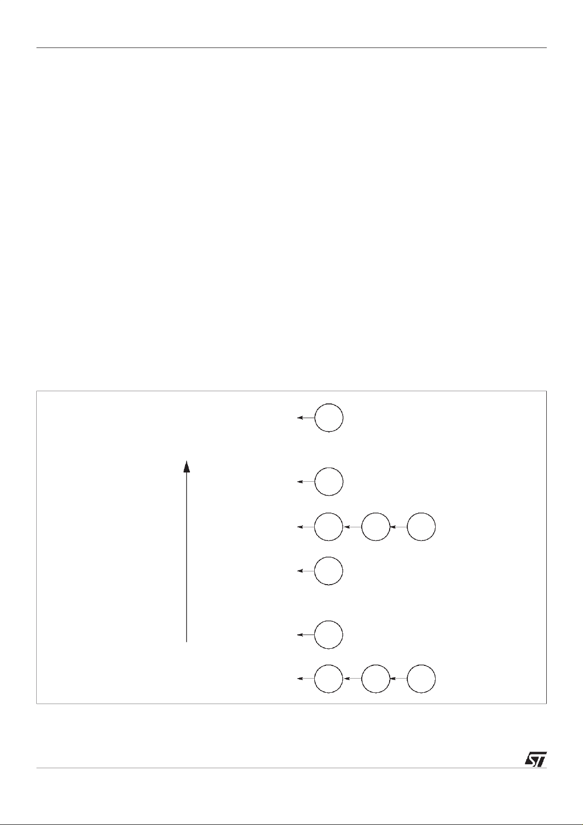
Figure 4.3 shows two processes waiting on the timer queue, one waiting for time 21, the other for
time 31.
Work spaces
ClockReg0
TnextReg0
TptrReg0
5
Comparator
21
Alarm
21
Program
Empty
31
Figure 4.3 Timer registers
4.6 Trapsand exceptions
A software error, such as arithmetic overflow or array bounds violation, can cause an error flag to
be set in the CPU.The flag is directly connected to the ErrorOut pin. Both the flagand the pin can
be ignored, or the CPU stopped. Stopping the CPU on an error means that the error cannot cause
further corruption. As well as containing the error in this wayit is possible to determine the state of
the CPU and its memory at the time the error occurred. This is particularly useful for postmortem
debugging where the debugger can be used to examine the state and history of the processor
leading up to and causing the error condition.
In addition, if a trap handler process is installed, a variety of traps/exceptions can be trapped and
handled by software. A user supplied trap handler routine can be provided for each high/low process priority level. The handler is started when a trap occurs and is given the reason for the trap.
The trap handler is not re-entrant and must not cause a trap itself within the same group. All traps
can be individually masked.
4.6.1 Trap groups
The trap mechanism is arranged on a per priority basis. For each priority there is a handler for each
group of traps, as shown in Figure 4.4.
24/123

Low priority traps High priority traps
ST20-GP6
Breakpoint
trap handler
CPU Error
trap handler
System operations
trap handler
Scheduler
trap handler
Figure 4.4 Traparrangement
There are four groups of traps, as detailed below.
• Breakpoint
This group consists of the
Breakpoint
trap. The breakpoint instruction (j0) calls the break-
point routine via the trap mechanism.
• Errors
The traps in this group are
IntegerError
and
flow, such as arithmetic results which do not fit in the result word.
errors caused when data is erroneous, for example when a range checking instruction finds
that data is out of range.
• System operations
This group consists of the
LoadTrap,StoreTrap
trap is signalled when an attempt is made to execute an illegal instruction. The
and
StoreTrap
traps allow a kernel to intercept attempts by a monitored process to change
or examine trap handlers or trapped process information. It enables a user program to signal to a kernel that it wishes to install a new trap handler.
CPU Error
trap handler
Breakpoint
trap handler
Overflow.Overflow
and
IllegalOpcode
Scheduler
trap handler
System operations
trap handler
represents arithmetic over-
IntegerError
traps. The
represents
IllegalOpcode
LoadTrap
• Scheduler
The scheduler trap group consists of the
TimeSlice, Run, Signal, ProcessInterrupt
ExternalChannel, InternalChannel, Timer,
and
QueueEmpty
traps. The
ProcessInterrupt
trap signals that the machine has performed a priority interrupt from low to high. The
QueueEmpty
trap indicates that there is no further executable work to perform. The other
traps in this group indicate that the hardware scheduler wants to schedule a process on a
process queue, with the different traps enabling the different sources of this to be monitored.
The scheduler traps enable a software scheduler kernel to use the hardware scheduler to
implement a multi-priority software scheduler.
Note that scheduler traps are different from other traps as they are caused by the microscheduler rather than by an executing process.
Trap groups encoding is shown in Table 4.3 below.These codes are used to identify trap groups to
various instructions.
25/123

ST20-GP6
Trapgroup Code
Breakpoint 0
CPU errors
System operations
Scheduler 3
1
2
Table 4.3 Trap group codes
In addition to the trap groups mentioned above,the CauseError flag in the Status register is used
to signal when a trap condition has been activated by the
causeerror
instruction. It can be used to
indicate when trap conditions have occurred due to the user setting them, rather than by the system.
4.6.2 Events that can cause traps
Table4.4 summarizes the events that can cause traps and gives the encoding of bits in the trap
Status and Enable words.
Trapcause
Breakpoint
IntegerError
Status/Enable
codes
00
1 1 Integer error other than integer overflow - e.g. explicitly checked or
Trap
group
Comments
When a process executesthe breakpoint instruction (j0) then it traps
to its trap handler.
explicitly set error.
Overflow
IllegalOpcode
LoadTrap
StoreTrap
InternalChannel
ExternalChannel
Timer
Timeslice
Run
Signal
ProcessInterrupt
QueueEmpty
CauseError
21
3 2 Attempt to executean illegal instruction. This is signalled when
42
52
63
7 3 Scheduler trap from external channel.
83
93
10 3 Scheduler trap from
11 3
12 3
13 3 Caused by no process active at a priority level.
15 (Status only) Any,
encoded
0-3
Integer overflowor integer division by zero.
executedwith an invalid operand.
When the trap descriptor is read with the
the trappedprocess status is read with the
When the trap descriptor is written with the
when the trapped process status is written with the
instruction.
Scheduler trap from internal channel.
Scheduler trap from timer alarm.
Scheduler trap from timeslice.
runp
(run process) or
Scheduler trap from
Start executing a process at a new priority level.
Signals that the
signal
causeerror
.
instruction set the trap flag.
ldtraph
ldtrapped
sttraph
startp
opr
instruction or when
instruction.
instruction or
sttrapped
(start process).
is
26/123
Table 4.4 Trapcauses and Status/Enable codes

ST20-GP6
4.6.3 Trap handlers
For each trap handler there is a trap handler structure and a trapped process structure. Both the
trap handler structure and the trapped process structure are in memory and can be accessed via
instructions, see section 4.6.4.
The trap handler structure specifies what should happen when a trap condition is present, see
Table4.5.
The trapped process structure saves some of the state of the process that was running when the
trap was taken, see Table4.6.
In addition, for each priority,there is an Enables register and a Status register. The Enables register contains flags to enable each cause of trap.The Status register contains flags to indicate which
trap conditions have been detected. The Enables and Status register bit encodings are given in
Table4.4.
Comments Location
Iptr Iptr of trap handler process. Base + 3
Wptr Wptr of trap handler process. A null Wptr indicates that a trap handler has not been installed. Base + 2
Status Contains the Status register that the trap handler starts with. Base + 1
Enables
A word which encodes the trap enable and global interrupt masks, which will be ANDed with
the existingmasks to allow the trap handler to disable various events while it runs.
Base + 0
Table4.5 Traphandler structure
Comments Location
Iptr Pointsto the instruction after the one that caused the trap condition. Base + 3
Wptr Wptr of the process that was running when the trap was taken. Base + 2
Status The relevant trap bit is set, see Table 4.3 for trap codes. Base + 1
Enables Interrupt enables. Base + 0
Table 4.6 Trapped process structure
A trap will be taken at an interruptible point if a trap is set and the corresponding trap enable bit is
set in the Enables register. If the trap is not enabled then nothing is done with the trap condition. If
the trap is enabled then the corresponding bit is set in the Status register to indicate the trap condition has occurred.
When a process takes a trap the processor saves the existing Iptr, Wptr, Status and Enables in
the trapped process structure. It then loads Iptr, Wptr and Status from the equivalent trap handler
structure and ANDs the value in Enables with the value in the structure. This allows the user to disable various events while in the handler, in particular a trap handler must disable all the traps of its
trap group to avoidthe possibility of a handler trappingto itself.
The trap handler then executes. The values in the trapped process structure can be examined
using the
ldtrapped
instruction (see section 4.6.4). When the trap handler has completed its opera-
27/123

ST20-GP6
tion it returns to the trapped process via the
tret
(trap return) instruction. This reloads the values
savedin the trapped process structure and clears the trap flag in Status.
Note that when a trap handler is started, Areg, Breg and Creg are not saved. The trap handler
must save the Areg, Breg, Creg registers using
stl
(store local).
4.6.4 Trap instructions
Trap handlers and trapped processes can be set up and examined via the
ldtrapped
and
sttrapped
instructions. Table4.7 describes the instructions that may be used when
ldtraph,sttraph
dealing with traps.
Instruction Meaning Use
ldtraph
sttraph
ldtrapped
sttrapped
trapenb
trapdis
tret
load trap handler Load the trap handler from memory to the trap handler descriptor.
store trap handler Store an existingtrap handler descriptor to memory.
load trapped Load replacement trapped process status from memory.
store trapped Store trapped process status to memory.
trap enable Enable traps.
trap disable Disable traps.
trap return Used to return from a trap handler.
,
causeerror
cause error Program can simulate the occurrence of an error.
Table 4.7 Instructions which maybe used when dealing with traps
The first fourinstructions transfer data to/from the trap handler structures or trapped process structures from/to an area in memory. In these instructions Areg contains the trap group code (see
Table4.3) and Breg points to the 4 word area of memory used as the source or destination of the
transfer. In addition Creg contains the priority of the handler to be installed/examined in the case of
ldtraphorsttraph. ldtrapped
If the
LoadTrap
trap is enabled then
LoadTrap trap flag. If the
and
sttrapped
StoreTrap
apply only to the current priority.
ldtraph
and
ldtrapped
trap is enabled then
do not perform the transfer but set the
sttraph
and
sttrapped
do not perform the
transferbut set the StoreTrap trap flag.
The trap enable masks are encoded by an array of bits (see Table 4.4) which are set to indicate
which traps are enabled. This array of bits is stored in the lower half-word of the Enables register.
There is an Enables register for each priority.Trapsare enabledor disabled by loading a mask into
Areg with bits set to indicate which traps are to be affected and the priority to affect in Breg. Executing
for the priority in Breg. Executing
trapenb
ORs the mask supplied in Areg with the trap enables mask in the Enables register
trapdis
negates the mask supplied in Areg and ANDs it with the
trap enables mask in the Enables register for the priority in Breg. Both instructions return the previous value of the trap enables mask in Areg.
28/123

ST20-GP6
4.6.5 Restrictions on trap handlers
There are various restrictions that must be placed on trap handlers to ensure that they work correctly.
1 Trap handlers must not deschedule or timeslice. Trap handlers alter the Enables masks,
therefore they must not allow other processes to executeuntil theyhave completed.
2 Trap handlers must have their Enable masks set to mask all traps in their trap group to
avoid the possibility of a trap handler trapping to itself.
3 Trap handlers must terminate via the
is that a scheduler kernel may use
restart
tret
(trap return) instruction.The only exception to this
to return to a previously shadowed process.
29/123
ST20-GP6
5 Interrupt controller
The ST20-GP6 supports external interrupts, enabling an on-chip subsystem or external interrupt
pin to interrupt the currently running process in order to run an interrupt handling process
The ST20-GP6 interrupt subsystem supports eight prioritized interrupts. This allows nested preemptive interrupts for real-time system design. In addition, there is an interrupt level controller
(refer to Chapter 6) which multiplexes incoming interrupts onto the eight programmable interrupt
levels.This multiplexing is controllable by software. There are 6 sources of interrupts. Four of these
are internal (2 for the UARTs,2 for the programmableIO) and two are external.
All interrupts are a higher priority than the low priority process queue. Each interrupt can be programmed to be at a lower priority or a higher priority than the high priority process queue, this is
determined by the Priority bit in the HandlerWptr0-7 registers, see Table 5.1 on page 33.
Note: Interrupts (Interrupt0-7) which are specified as higher priority must be contiguous from the
highest numbered interrupt downwards,i.e. if 4 interrupts are programmed as higher priority and 4
as lower priority the higher priority interrupts must be Interrupt7:4 and the lower priority interrupts
Interrupt3:0.
Note that interrupt handlers must not prevent the GPS DSP data traffic from being handled. During
continuous operation this has 1 ms latency and is not a problem, but during initial acquisition it has
a32µs rate and thus care must be taken with interrupt priorities unless used to stop GPS opera-
tion.
Interrupt 7
when Priority bit set to 0
..
.
.
Interrupt 0
when Priority bit set to 0
High priority
Increasing
pre-emption
process
Interrupt 7
when Priority bit set to 1
..
.
.
30/123
Interrupt 0
when Priority bit set to 1
Low priority
process
Figure 5.1 Interrupt priority
 Loading...