SGS Thomson Microelectronics ST207E Datasheet

■ ESDPROTECTIONFORRS-232I/OPINS:
±
15KV HUMANBODYMODEL
■ GUARANTEED120kbpsDATERATE-
LapLink COMPATIBLE
■
GUARANTEEDSLEWRATE3V/µs (Min)
■ OPERATEFROMA SINGLE5VPOWER
SUPPLY
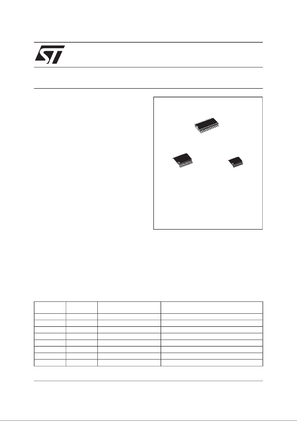
■ PACKAGEDINSO-24,SSO-24AND TSSOP24
PACKAGES
DESCRIPTION
The ST207E is a 5 driver and 3 receiver devices
designedforRS-232 and V.28 communicationsin
harsh enviroments. Each transmitter output and
receiver input is protected against±15KV
electrostaticdischarge (ESD) shocks. The drivers
and receivers of the ST207E meet all
EIA/TIA-232E and CCITT V.28 specifications at
data rates up to 120Kbps, when loaded in
accordancewith the EIA/TIA-232Especification.
The ST207E operateswith four 0.1µF capacitors.
It cames in 24-pinSO and TSSOPpackages.
ST207E
± 15KVESD PROTECTED
5V RS-232 TRANSCEIVER
PRELIMINARY DATA
D
(Micro Package Large)
P
(SSOPPackage)
(TSSOPPackage)
T
ORDERCODES
Type Temperature
Range
ST207ECD 0 to 70
ST207EBD -40 to 85
ST207ECDR 0 to 70
ST207EBDR -40 to 85
ST207ECTR 0 to 70
ST207EBTR -40 to 85
ST207ECPR 0 to 70
ST207EBPR -40 to 85
June 2000
Package Comments
o
C SO-24 (Tube) 33 partsper tube / 25 tube per box
o
C SO-24 (Tube) 33 partsper tube / 25 tube per box
o
C SO-24 (Tape & Reel) 1000 parts per reel
o
C SO-24 (Tape & Reel) 1000 parts per reel
o
C TSSOP24 (Tape & Reel) 2500 parts per reel
o
C TSSOP24 (Tape & Reel) 2500 parts per reel
o
C SSOP24 (Tape & Reel)
o
C SSOP24 (Tape & Reel)
1/9

ST207E
PIN CONFIGURATION
PIN DESCRIPTION
PIN No SYM BO L NAM E AND FUNC T I O N
1T3
2T1
3T2
4R1
5R1
6T2
7T1
OUT
OUT
OUT
IN
OUT
IN
IN
8 GND Ground
9V
10 C
CC
+ Terminal For Positive Charge-pump Capacitor
1
11 V+ 2V
12 C
13 C
14 C
- Terminal For Positive Charge-pump Capacitor
1
+ Terminal For Negative Charge-pump Capacitor
2
+ Terminal For Negative Charge-pump Capacitor
2
15 V- -2V
16 R3
17 R3
18 T3
19 T4
20 T5
21 T5
22 R2
23 R2
IN
OUT
IN
IN
OUT
IN
OUT
IN
RS-232 Driver Output
RS-232 Driver Output
RS-232 Driver Output
RS-232 Receiver Input
TTL/CMOS Receiver Outputs. All The Receivers Are Inactive In Sutdown
TTL/CMOS Driver Inputs. Internal Pull-up to V
TTL/CMOS Driver Inputs. Internal Pull-up to V
4.75V to 5.25V Supply Voltage
Generated By The Charge Pump
CC
Generated By The Charge Pump
CC
RS-232 Receiver Input
TTL/CMOS Receiver Outputs. All The Receivers Are Inactive In Sutdown
TTL/CMOS Driver Inputs. Internal Pull-up to V
TTL/CMOS Driver Inputs. Internal Pull-up to V
RS-232 Driver Output
TTL/CMOS Driver Inputs. Internal Pull-up to V
TTL/CMOS Receiver Outputs. All The Receivers Are Inactive In Sutdown
RS-232 Receiver Input
CC
CC
CC
CC
CC
2/9

ST207E
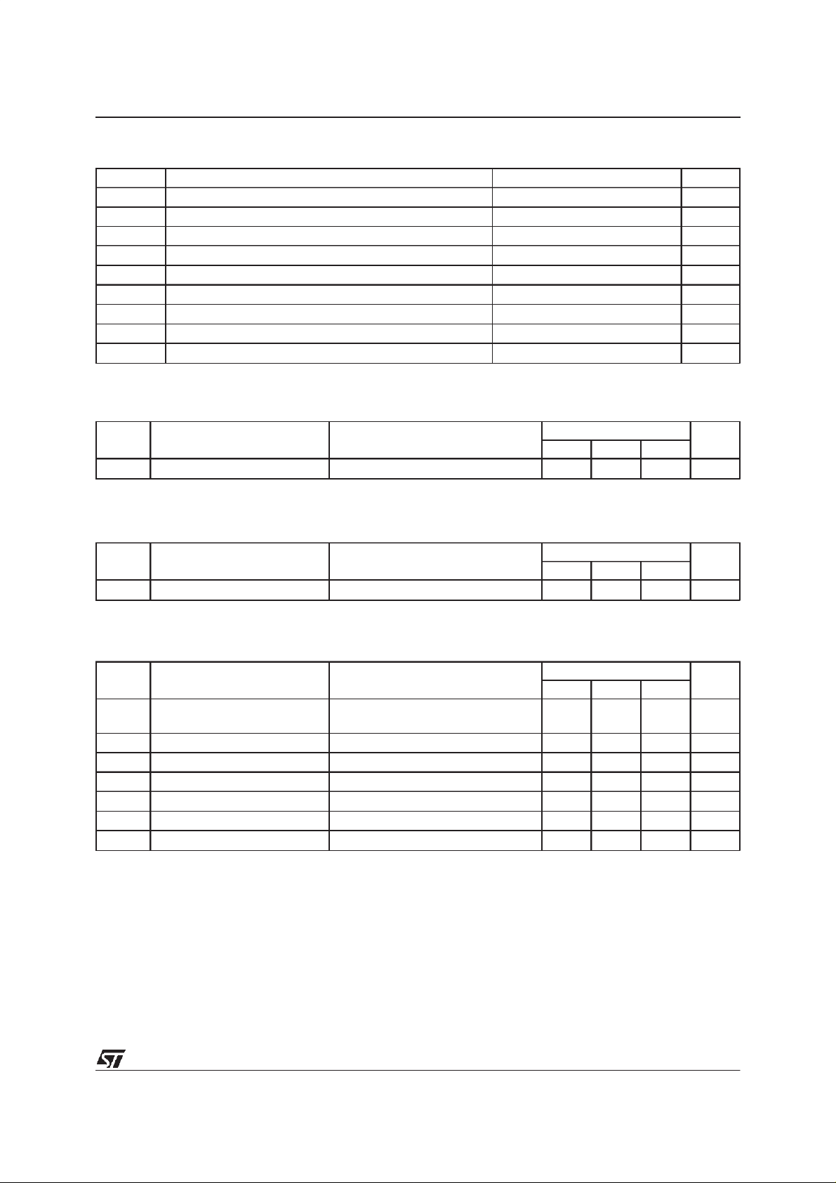
ABSOLUTE MAXIMUM RATINGS
(Note 1)
Symb o l Para met er Val u e Uni t
V
V
V
T
R
T
OUT
R
OUT
T
SCTOUT
T
AbsoluteMaximumRatingsarethosevaluesbeyond whichdamagetothedevicemayoccur. Functionaloperationunderthese condition isnotimplied.
Supply Voltage -0.3 to 6 V
CC
Extra Positive Voltage (VCC-0.3) to 14 V
+
Extra Negative Voltage -14 to 0.3 V
-
Transmitter Input Voltage Range -0.3 to (VCC+ 0.3) V
IN
Receiver Input Voltage Range ±30 V
IN
Transmitter Output Voltage Range (V- - 0.3) to (V+ + 0.3) V
Receiver Output Voltage Range -0.3 to (VCC+ 0.3) V
Short Circuit Duration on T
Storage Temperature Range -65 to +150
stg
OUT
Continuous
o
C
ESD PERFORMANCE: TRANSMITTEROUTPUTS, RECEIVER INPUTS
Symbol Parameter Test Conditions Value Unit
Min. Typ. Max.
ESD ESD Protection Voltage Human Body Model ±15 kV
ELECTRICAL CHARACTERISTICS
(C
otherwisespecified. Typical Valus are referredto T
Symbol Parameter Test Conditions Value Unit
I
SUPPLYVCC
Power Supply Current No Load, TA=25oC25mA
= 0.1µF, VCC=5V±5% TA= Min to Max,unless
1-C4
=25oC)
A
Min. Typ. Max.
RECEIVERELECTRICAL CHARACTERISTICS(C1-C4= 0.1µF, VCC=5V±5% TA= Min to Max,
unlessotherwise specified.TypicalValus are referred toT
Symbol Parameter Test Conditions Value Unit
V
V
V
V
R
Receiver Input Voltage
RIN
Operating Range
Input Threshold Low TA=25oC, VCC= 5 V 0.8 1.2 V
RIL
Input Threshold High TA=25oC, VCC= 5 V 1.7 2.4 V
RIH
Input Hysteresis VCC= 5 V, no hysteresis in shutdown 0.2 0.5 1 V
RIHYS
Input Resistance TA=25oC, VCC=5V 357K
RIN
Output Voltage Low 0.4 V
V
OL
Output Voltage High I
V
OH
= -1mA 3.5 VCC-0.4 V
OUT
=25oC)
A
Min. Typ. Max.
-30 30 V
Ω
3/9
 Loading...