

SGS Thomson Microelectronics ST19CF68 Datasheet
With 512 Bits Modular Arithmetic Processor
■ 8 BIT ARCHITECTURE CPU
■ 23 KBytes of USER ROM WITH
PARTITIONING
■ SYSTEM ROMFOR LIBRARIES
■ 960 Bytes of RAM WITH PARTITIONING
■ 8 KBytes of EEPROM WITH PARTITIONING
– Highly reliable CMOS EEPROM technology
– 10 year data retention
– 100,000 Erase/Write cycle endurance
– Separate Write and Erase cycles for fast “1”
programming
– 1 to 64 bytes Erase or Program in 1 ms
■ 512 BITS MODULAR ARITHMETIC
PROCESSOR
– Fast modular multiplication and squaring us-
ing Montgomery method
– Software Crypto Libraries in separate ROM
area for efficient algorithm coding using a set
of advanced functions
– Software selectable operand length
up to 1024 bits
■ SECURITY FIREWALLS FORMAP AND
MEMORIES
■ VERY HIGH SECURITY FEATURES
INCLUDING EEPROM FLASH PROGRAM
AND RAM FLASH CLEAR
■ 8 BIT TIMER
■ SERIAL ACCESS, ISO 7816-3 COMPATIBLE
■ 3V ± 10% or 5V± 10% SUPPLY VOLTAGE
■ POWER SAVING STANDBY MODE
■ UP TO 10 MHz INTERNAL OPERATING
FREQUENCY
■ CONTACT ASSIGNMENT COMPATIBLE ISO
7816-2
■ ESD PROTECTION GREATER THAN 5000V
■ FAST CRYPTOGRAPHIC FUNCTIONS
PROCESSING (5V± 10%, 5MHz)
ST19CF68
Smartcard MCU
DATA BRIEFING
2
2
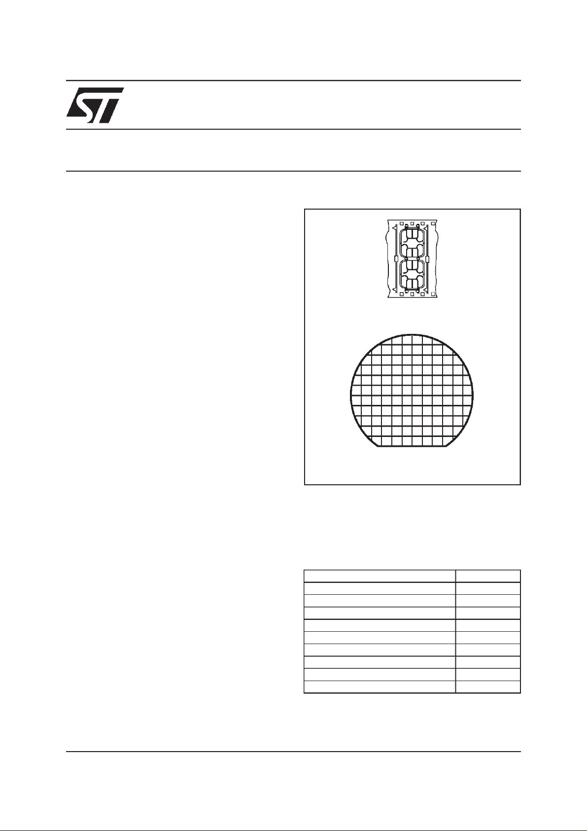
Micromodule (D4)
Function Speed
RSA 512 bits signature with CRT * 70 ms
RSA 512 bits signature without CRT 200 ms
RSA 512 bits verification (e=$10001) 6 ms
RSA 768 bits signature with CRT 200 ms
RSA 768 bits signature without CRT N/A
RSA 768 bits verification (e=$10001) 100 ms
RSA 1024 bits signature with CRT 400 ms
RSA 1024 bits signature without CRT N/A
RSA 1024 bits verification (e=$10001) 150 ms
*CRT: Chinese Remainder Theorem
2
2
Wafer
BD.CF68/9809VP5
This is Brief Datafrom STMicroelectronics.Details are subject tochange without notice. Forcomplete data, pleasecontact
your nearestSales Office or SmartCard ProductsDivison, Rousset, France. Fax: (+33) 4 42 25 8729
1/2
ST19CF68
HARDWARE DESCRIPTION
The ST19CF68, a member of the ST19 device
family, isa serial access microcontroller especially
designed for very large volume and cost competitive secure portable objects, where high performance Public Key Algorithms will be implemented,
to cut down initialization and communication costs
and to increase security.
Its internal Modular Arithmetic Processor is designed to speed up cryptographic calculations using Public Key Algorithms. Based on a 512 bit
architecture, it processes modular multiplication
and squaring up to1024 bit operands.
The ST19CF68 is based on a STMicroelectronics
8 bit CPU core including on-chip memories: 960
Bytes of RAM, 23 KBytes of USER ROM and 8
KBytes of EEPROM.
RAM, ROM and EEPROM memories can be configured into partitions. Access rules from any
memory partition to another partition are setup by
the user defined Memory Access Control Logic.
It is manufactured using the highly reliable ST
CMOS EEPROM technology.
As all other ST19 family members, it is fully compatible with theISO standards forSmartcard applications.
SOFTWARE SUPPORT
SOFTWARE DEVELOPMENT
Software development and firmware (ROM code/
options) generation are completed by the ST16-19
HDS development system.
CRYPTO LIBRARIES
For an easy and efficient use of the Modular Arith-
metic Processor (MAP), ST proposes a complete
set of firmware subroutines. This library is located
in a specific ROM area, leaving 23 KBytes in the
User ROM for the application software. This library saves the operating system designer from
coding first layer functions and allows the designer
to concentrate on algorithms and Public KeyCryptographic (PKC) protocol implementation.
This library contains firmware functions for:
– loading and unloading parameters and results
to or from the MAP
– calculating Montgomery constants
– basic mathematics including modular squaring
and multiplication for various lengths
– modular exponentiation using or not the Chi-
nese Remainder Theorem (CRT),
– more elaborate functions such as RSA signa-
tures and authentications for any modulo length
up to 1024 bits long or DSA signature and veri-
fication.
– full internal key generation for signatures/au-
thentications. This guarantees that the secret
key will never be known outside the chip and
contributes to overall system security.
– long random number generation
– sha-1
Figure 1. Block Diagram
a
2/2
RAM
960 8 K
Bytes
CLOCK
GENERATOR
MODULE
CLK
EEPROM
MEMORYACCESS FIREWALL
8 BIT
TIMER
Bytes
USER
ROM
23 K
Bytes
SECURITY
ADMINISTRATOR
RESET VCC I/OGND
SYSTEMROM
INTERNALBUS
UNPREDICTABLE
NUMBER
GENERATOR
AND
CRYPTO
LIBRARIES
512 Bits
SYSTEMROM
AND
MAP FIREWALL
8 BIT
CPU
MAP
SERIAL
I/O
INTERFACE
SCP 133b/DS
a
 Loading...