

SGS Thomson Microelectronics ST18D952 Datasheet

12 January 98 42 1714 01
The information in this datasheet is subject to change 1/66
ST18952
DIGITAL SIGNAL PROCESSOR (DSP) CHIP
PRELIMINARY DATA
■ Programmable D950 Core
■ Data calculation unit
■ Address calculationunit
■ Program control unit
■ Fast and flexible buses
■ 66MIPS - 15 ns instruction cycle time
■ 16.5 Kwords data memory (RAM)
■ 32 Kwords program memory (RA42 1714 01)
■ Interrupt controller
■ DMA controller
■ Serial input/output
■ Timer
■ Bus switch unit
■ Emulation unit
■ JTAG IEEE 1149.1 test access port
TAP
Emulation
unit
2
Timers
2
Serial I/O
Interrupt
controller
16.5 Kwords
data memory
Bus switch
unit
DMA
controller
D950
core
32 Kwords
program
memory

2/66
Table of Contents
3
1 Introduction . . . . . . . . .................................................. 4
2 Pin Description . . . . . ..................................................5
3 Functional Overview . . . . . . . . . . . . . . . . . . .................................9
4 D950Core ..........................................................12
4.1 D950Core registers . . . . . . . . ....................................... 14
5 Memory ............................................................ 15
5.1 Internal memory resource . . . ....................................... 15
5.2 Direct bus extension . . . . . . . . . . . . . . . . . . . . . . . . . .....................16
6 Bus Switch Unit . . . . . . . . . . . . . . . . . . . . . . . . . ............................. 18
6.1 BSUoperation ................................................... 18
6.2 BSU control registers . . . . . . . ....................................... 19
7 DMA Controller . . . . . ................................................. 21
7.1 DMA operation . . . . ...............................................22
7.2 DMA registers . . . . . . . ............................................23
8 Interrupt Controller . . . . . ............................................... 26
8.1 Interrupt controller registers . . . . . . . . .................................27
9 Timers ............................................................. 31
9.1 Timerregisters................................................... 31
10 SIO ...............................................................35
10.1 SIO registers . . . . . . . . . . . . . . . . . ...................................35
11 External Coprocessor . . . . . ............................................41
12 SystemControl ......................................................41
12.1 System registers .................................................42
12.2 Clocks . . . . . . . . . . . . . . . . . . . . . . . . . . . . . . . ..........................44
13 JTAG IEEE 1149.1 test access port ...................................... 45
14 Emulation Unit . . . . . . .................................................45
15 Electrical Specifications ................................................47
15.1 DC Absolute maximum ratings ...................................... 47
15.2 DC Electrical characteristics . . . . . . . . . . . . . . . . ........................47
15.3 AC Characteristics . . . .............................................48
16 Y SPACE Memory Mapping . . . . . ....................................... 56
16.1 Memorymap ....................................................56
16.2 Serial input/output registers . . . . . . . . . . . . . . . . . ........................56
16.3 Timerregisters...................................................58
16.4 Bus switch unit registers . . . . . . . . . . .................................58
1

3/66
Table of Contents
16.5 System control registers . . . . . . . . . . ................................. 58
16.6 DMA controller registers . . . . . . . . . . . . . ..............................59
16.7 Interrupt controller registers . . . . . . . . . . . . . . . . . . . . . . . . . . . . .............59
16.8 Emulation unit registers . . . . . . . . . . . . . . .............................. 60
16.9 D950Core control registers . . . . . . . . . . . . . . . . . . . . . . . .................. 60
17 ST18952 Package Specifications . .......................................61
17.1 208 pin PQFP pinout . . . . . . . . . . ....................................61
17.2 208 pin PQFP package dimensions . . . . . .............................62
18 DeviceID...........................................................64
19 Ordering Information . . . . . . . . . . . . ......................................64
20 Revision History . . . . . . . ............................................... 64

4/66
ST18952
1 Introduction
The ST18952 chip includes the SGS-Thomson D950 16-bit fixed point digital signal processor
core, 16.5 Kwords of data memory, 32 Kwords of program memory, and the following on-chip
peripherals:
• Interrupt controller (ITC)
• DMA controller (DMA)
• Bus switch unit (BSU)
• Synchronous input/output (SIO)
• Timer (TIM)
• Emulation unit (EMU)
• Tap controller (TAP)
It also includes an oscillator and a PLL for generation of the D950Core clock.
The ST18952 is used on the D950 Emulation Card (called the D952 module) developed by
SGS-Thomson.
It can also be used for application development by customers.
Custom development is eased by providing direct access to the D950 instruction and data
buses to allow simultaneous access to external memories or peripherals (with wait-states).
For full details of the D950Core refer tothe D950Core datasheet (
document number 42-1709
).
2

5/66
ST18952
2 Pin Description
The following tables detail the ST18952 pin set. There is one table for each group of pins. The
tables detail the pin name, type and a short description of the pin function.
Signal names have an overbar if they are active low, otherwise they are active high.
Table 2.1 Direct I bus extension (35 pins)
Table 2.2 Direct Y bus extension (35 pins)
Table 2.3 Direct X bus extension / bus extension through bus switch unit (39 pins)
Pin name Type Description
IDE0-15 I/O Instruction data extension bus.
IAE0-15 O Instruction address extension bus.
IRDE O I-extension bus read strobe. Active low.
IWRE O I-extension bus write strobe. Active low.
IBSE O I-extension bus strobe. Active low.
Pin name Type Description
YDE0-15 I/O Y data extension bus.
YAE0-15 O Y address extension bus.
YRDE O Y-extension bus read strobe. Active low.
YWRE O Y-extension bus write strobe. Active low.
YBSE O Y-extensionbus strobe. Active low.
Pin name Type Description
ED_XDE0-15 I/O Multiplexed input/output. Bus switchunit extension data bus or X data exten-
sion bus.
EA_XAE0-15 O Multiplexed output. Bus switch unit extension address bus or X address ex-
tension bus.
EIRD O BSU EIRD output
EIWR O BSU EIWR output
XBSE O X extension bus data strobe
EYRD O BSU EYRD output
EYWR O BSU EYWR output
XRDE_EXRD O Multiplexed output.
X-extension bus read strobe (XRDE) or BSU EXRD output.
XWRE_EXWR O Multiplexed output.
X-extension bus write strobe (XWRE) or BSUEXWR output.

6/66
ST18952
Table 2.4 General purpose parallel port / Interrupt requests (8 pins)
Table 2.5 Clocks (6 pins)
Table 2.6 Bus control (3 pins)
Pin name Type Description
P_ITRQ0-7 I/O Multiplexed input/output. Parallel port I/O or external interrupt request (ITRQ).
Pin name Type Description
EXTAL I Oscillator input.
XTAL O Oscillator output. Nominal oscillator frequency is 27 MHz.
MCLK I Master clock input (use of external clock generator).
CLK_MODE I Clock mode select input.
When low the oscillator and internal PLL are enabled. The 950 receives its
Master clock from the PLL at 5 times the oscillator frequency.
When high the PLL is disabled. The D950 receives its master clock from
MCLK.
INCYCLE O Instruction cycle.
Asserted high for 1 CLKOUT cycle at the beginning of instruction cycle.
CLKOUT O Output clock (at input clock/2 frequency).
Pin name Type Description
DTACK I Data transfer acknowledge input. Active low.
It is combined in a ORgate with BSU DTACK output in order to generate the
DTACK signal for the D950Core. It controls extension of bus cycles by inser-
tion of wait-states whenusing external memory either through Bus-switch or
direct extension.
HOLD I External Bus Hold request input. Active low.
HOLDACK O Hold acknowledge output. Active low.

7/66
ST18952
Table 2.7 D950Core control (10 pins)
Table 2.8 Emulation unit (7 pins)
Pin name Type Description
RESET I Reset input. Active low.
Initializes the 950-Core to the RESET state.
RESET_OUT O Reset output (system reset). Active low.
LP I Low power input. Active low.
LPACK O Low power acknowledge. Active low.
MODE I Mode selection for Reset.
0: forces reset address to 0x0000
1: forces reset address to 0xFC00
IRD_WR O Program memory read/write indicator.
VCI O Valid coprocessor instruction output.
Asserted low during the instruction cycle preceding a coprocessor instruc-
tion to enable operation of an external coprocessor.
STACKX O X stack read/write instruction flag.
STACKY O Y stack read/write instruction flag.
IDT_EN I I-bus direct transfer enable (to BSU peripheral). Active low.
Pin name Type Description
ERQ I Emulator Halt Request. Active low.
Halts program execution and enters emulation mode.
IDLE O Output flag assertedhigh when the processoris halted dueto an emulation
halt request or a valid breakpoint condition.Asserted low when the processor is not Halted or during execution ofan instruction under control of the
emulator.
HALTACK O Halt acknowledge. Active high.
Asserted highwhen the processor is halted from anEmulator Halt request
or when a valid Breakpoint condition is met.
SNAP O Snapshot. Active high.
Asserted highwhen executing an instructionif Snapshot modeis enabled.
AXEBP I Enable breakpoint on X address buswhen high.
AYEBP I Enable breakpoint on Y address buswhen high.
AIEBP_SCAN_EN I Enable breakpoint on I address bus when high.

8/66
ST18952
Table 2.9 JTAG IEEE 1149.1 test access port (5 pins)
Table 2.10 DMA controller / Serial input/output (8 pins)
Pin name Type Description
TDI I Test data input.
TCK I Test clock.
TMS I Test mode select.
TDO O Test data output.
TRST I Test logic reset (also used for Emulator module). Active low.
Pin name Type Description
DMARQ0/SRD0 I DMA request 0or SIO0 Receive data
DMARQ1/SCK0 I/O DMA request 1 or SIO0 Data clock
DMARQ2/SRD1 I DMA request 2or SIO1 Receive data
DMARQ3/SCK1 I/O DMA request 3 or SIO1 Data clock
DMACK0/STD0 O DMA acknowledge 0 or SIO0 Transmit data
DMACK1/SFS0 I/O DMA acknowledge 1 or SIO0 Frame synchronizer
DMACK2/STD1 O DMA acknowledge 2 or SIO1 Transmit data
DMACK3/SFS1 I/O DMA acknowledge 3 or SIO1 Frame synchronizer
9/66
ST18952
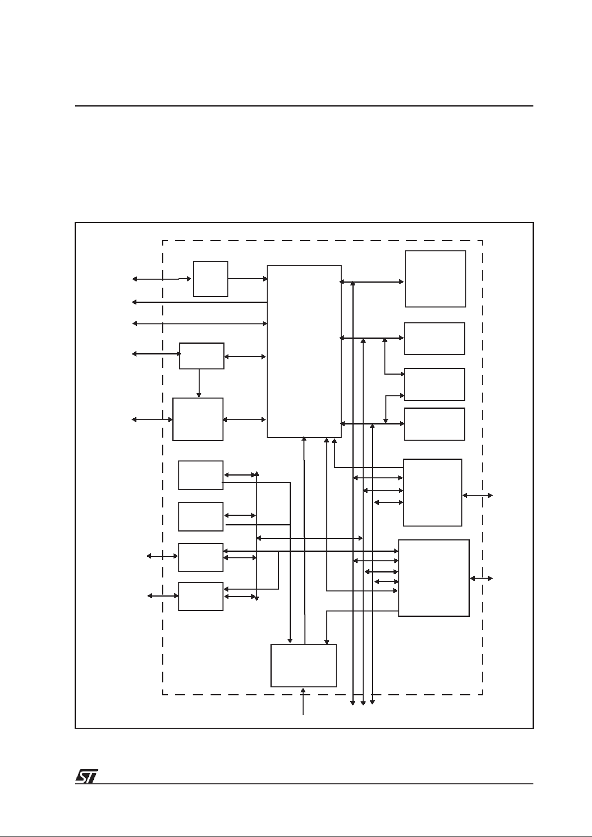
3 Functional Overview
A block diagram of the ST18952 isshown below. The modules that comprise the ST18952 are
outlined in this section and described in detail in the following sections.
Figure 3.1 ST18952 block diagram
Y
X
D950Core
DMA
TAP
Interrupt
8k x 16
Bus
8k x 16
8k x 16
I
OSC
+
PLL
X/Y
0.5k x 16
Emulation
Control I/Os/ Port
JTAGPort
(x 4)
Output clocks
Input clock + control
Timer 0
SIO 1
Timer 1
SIO 0
controller
switch
unit
unit
controller
Direct extension buses
Ext. bus

10/66
ST18952
D950Core
The D950Core is a general purpose programmable 16-bit fixed point Digital Signal Processor
Core. The main blocks of the D950Core include an arithmetic data calculation unit, a program
control unit and an address calculation unit, able to manage up to 64k (program) and 128k
(data) x 16-bit memory spaces.
Memory
One 32 Kword and two 8 Kword single port memories are included on-chip:
• 32 Kword instruction memory on I space
• 8 Kword X-Data memory on X space
• 8 Kword Y-Data memory on Y space
One 512 word dual port memory is shared on X and Y spaces.
Memory can be extended off-chip for all three spaces in two ways:
1: Directly - Accesses to program and data memories can be performed simulta-
neously. Insertion of wait-states is necessary in case of nominal frequency
work.
2: Through the bus switch unit - Accesses to the different external spaces are mul-
tiplexed and wait-states are added.
Bus switch unit
The bus switch unit (BSU) is a bi-directional switcher which switches the 3 internal buses (I, X
and Y) to the external (E) bus.
DMA controller
The DMA controller manages data transfer between memories and external peripherals.
There are four independent DMA channels. Transfers can occur on X/Y/I spaces
(simultaneous transfers on X and Y spaces).
Interrupt controller
The interrupt controller (ITC) can manage up to eight external interrupts. Each source can be
individually activated and programmed as edge or level triggered. A ‘pending interrupt’ flag
displays the source waiting for service (this flag is writable to allow a software interrupt
capability). The priority of interrupts is programmable.
Timers
There are two timer (TIM) units on the ST18952. The timers enable interrupts to be generated
after predefined periods of time.

11/66
ST18952
SIO
There are two synchronous serial input/output (SIO) ports enable a link to serial devices such
as codecs and to other processors.
Oscillator and PLL
A 27 MHz crystal can be used with the on-chip oscillator and PLL to provide the D950Core
clock input. The PLL module multiplies the oscillator frequency by a factor of 10 and generates
a 270 MHz signal. A programmable divider is connected to the PLL output to generate the
D950 clock input. The division range is 2 to 256.
Emulation unit and JTAG IEEE 1149.1 test access port
The emulation unit (EMU) performs functions dedicated to emulation and test through the
external IEEE 1149.1 JTAG interface.

12/66
ST18952
4 D950Core
The D950Core is composed of three main units.
• Data Calculation Unit (DCU)
• Address Calculation Unit (ACU)
• Program Control Unit (PCU)
For full details of the D950 DSP core refer to the D950Core datasheet (
document number 42-
1709
).
These units are organized in an HARVARD architecture around three bidirectional 16-bit
buses, two for data and one for instruction. Each of these buses is dedicated to an unidirectional 16-bit address bus (XA/YA/IA).
An 8-bit general purpose parallel port (P0-P7) can be configured (input or output). A test
condition is attached to each bit to test external events.
The D950Core is controlled through interface pins related to interrupt, low-power mode, reset
and miscellaneous functions.
Figure 4.1 D950Core block diagram
DATA
CALCULATION
UNIT
ADDRESS
CALCULATION
UNIT
PROGRAM
CONTROL
UNIT
CLKIN
DATA MEMORY
PROGRAM MEMORYVDD
VSS
TEST & EMULATIONPO/P7
CONTROL
11
8
14
XD-bus
YD-bus
6
16
16
16
16
3
16
16
OUTPUT
CLOCKS
XA-bus
YA-bus
ID-bus
IA-bus
Control
13/66
ST18952
Data buses (XD/YD and XA/YA) are provided externally. Data memories (RAM, ROM) and
peripherals registers are mapped in these address spaces.
Instruction bus (ID/IA) gives access to program memory (RAM, ROM). Each bus has its own
control interface.
Table 4.1 Data/instruction bus and corresponding address bus.
Depending on the calculation mode, the D950Core DCU computes operands which can be
considered as 16 or 32-bit, signed or unsigned. It includes a 16 x 16-bit parallel multiplier able
to implement MAC-based functions in one cycle per MAC. A 40-bit arithmetic and logic unit,
including an 8-bit extension for arithmetic operations, implements a wide range of arithmetic
and logic functions. A 40-bit barrel shifter unit and a bit manipulation unit are included.
The tables below illustrate the different types of word length and word format available for
manipulation.
Table 4.2 Summary of possible word lengths and formats
Data/instruction bus Corresponding address bus
XD Bidirectional 16-bit XA Unidirectional 16-bit
YD Bidirectional 16-bit YA Unidirectional 16-bit
ID Bidirectional 16-bit IA Unidirectional 16-bit
0 1-bit word
7 0 8-bit word
15 0 16-bit word signed / unsigned
31 16 15 0 32-bit word signed / unsigned
39 32 31 16 15 0 40-bit word signed / unsigned
Format Minimum Maximum
fractional signed - 1 + 0.999969481
unsigned 0 + 0.99996948
integer signed - 32768 + 32767
unsigned 0 + 65535

14/66
ST18952
4.1 D950Core registers
PCDR
The Port Control Direction register defines the data direction of each port pin. After reset,
PCDR default value is 0 (Port pins are configured as inputs)
PCSR
The Port Control Sensitivity register defines sensitivity of each port pin. After reset, PCSR
default value is 0 (Port pins are configured as level-sensitive).
Register Function
BX Modulo base address for X-memory space
MX Modulo maximum address for X-memory space
BY Modulo base address for Y-memory space
MY Modulo maximum address for Y-memory space
POR Port Output Register - 8LSB are significant, 8MSB are undefined when reading
PIR Port Input Register
PCDR Port Control Direction Register
PCSR Port Control Sensitivity Register
1514131211109876543210
--------P7DP6DP5DP4DP3DP2DP1DP0D
Bit Function
PiD Port pin direction
0: Input port pin (def.)
1: Output port pin
Bits 8 - 15 RESERVED (read: undefined, write: don’t care)
1514131211109876543210
--------P7SP6SP5SP4SP3SP2SP1SP0S
Bit Function
PiS Port pin sensitivity
0: Level sensitive (def.)
1: Edge sensitive
Bits 8 - 15 RESERVED (read: undefined, write: don’t care)
15/66
ST18952
5 Memory
5.1 Internal memory resource
One 32 Kword and two 8 Kword single port memories are included on-chip:
• Instruction memory on I space from address 0 to 32767 (32 K)
• X-Data memory on X space from address 0 to 8191 (8 K)
• Y-Data memory on Y space from address 0 to 8191 (8 K)
One 512 word dual port memory is shared on X and Y spaces, from addresses 8192 (8 K) to
8703 (8.5K). This is represented graphically below.
Note: the first 256 addresses of the Y space are reserved for the D950 memory-mapped
registers and for on-chip memory mapped peripherals.
Memory can be extended off-chip for all three spaces in two ways:
1: Directly - Accesses to program and data memories can be performed simulta-
neously. Insertion of wait-states is necessary in case of nominal frequency
work.
2: Through the bus switch unit - Accesses to the different external spaces are mul-
tiplexed and wait-states are added.
The specific details on the operation of the BSU are described separately in ”Bus Switch Unit”
on page 18.
Figure 5.1 Memory mapping
0000
1FFF 8k
32k
FFFF
64k
64k
Internal SPRAM
Internal SPRAM
Registers
External
Internal SPRAM
ExternalExternal
All addresses are hexadecimal
Internal DPRAM
Internal DPRAM
21FF
8.5k
0100
64k
8k
8.5k
FFFF
8000
1FFF
FFFF
21FF
External memory is accessed directly or through the bus switch
X-memory I-memoryY-memory

16/66
ST18952
5.2 Direct bus extension
Direct extension for I-memory
The internal program memory is used from address 0 to 32767 (32 K). Note, no detection is
provided when an internal space is declared as an external one for the BSU.
The I-bus direct transfer enable signal (IDT_EN) determines whether an access is made
directly to external memory or via the BSU. If reset occurs with the MODE signal set to ‘1’
(select reset address to xFC00), then
• if IDT_EN input = 0: access to external memory is through the BSU
• if IDT_EN input = 1: access to direct external memory space
IAE/IBSE/IRDE/IWRE are always driven except in the case of an external HOLD request.
Note: an external coprocessor will work only when executing program in the external space.
IDE bus is an output only when a direct external write is detected. IDE bus is an input in the
case of:
• an external memory read
• DMA (write) transfers between an external peripheral and internal memory
Direct extension for X-memory
The internal X memory is used from address 0 to 8703 (8.5 K). It is extended with external
memory from address 8704 (8.5K) to 65535 (64K) with the XE bus extension.
The direct extension is managed by the bus switch unit. When the EN_X bit of the BSU XER
register (see ”XER0/1: X-memory space control registers” on page 20) isset to ‘0’, it generates
only software wait-states and access is direct. If the EN_X bit is set to ‘1’, data goes via the
BSU.
X extension and bus switch share the same I/O’s.
Direct extension for Y-memory
The internal Y memory is used from address 0 to 8703 (8.5 K). It is extended with external
memory from address 8704 (8.5 K) to 65535 (64 K) with the YE bus extension.
Address 0 to 256 of the Y space are reserved for memory mapped registers.
Note: The BSU and X direct extension share the same I/O, therefore extension of IE through
the BSU is not possible when direct extension is selected for X/Y. Some combinations of the
EN_I, EN_X and EN_Y bits of the BSU control registers IER/XER/YER are not allowed, as
shown in Table 5.1 below.

17/66
ST18952
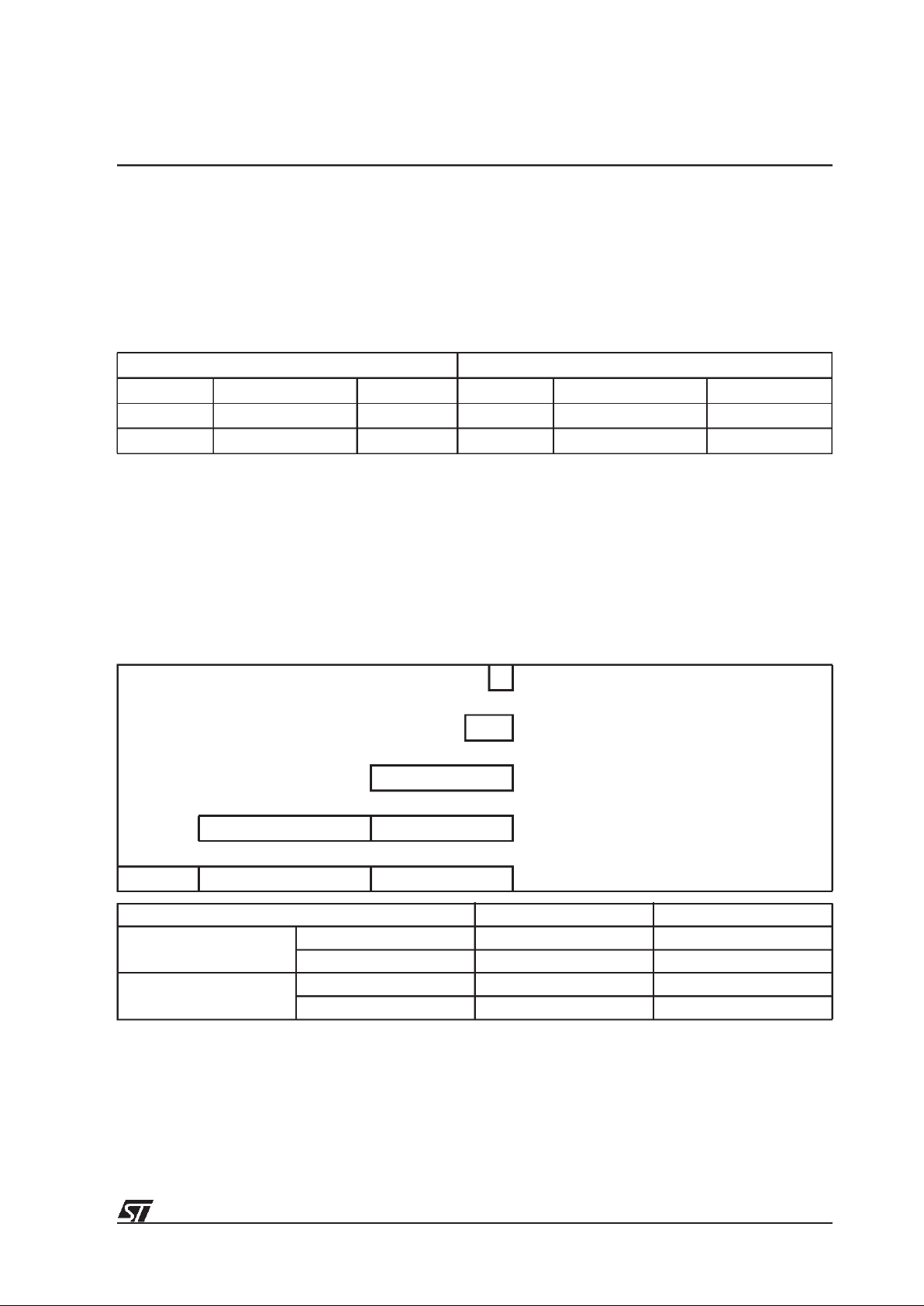
Table 5.1 Possible BSU register settings
EN_I EN_X EN_Y Operation Allowed or forbidden
1 1 1 Exchanges enabled on I/X/Y spaces Allowed
1 1 0 Exchanges enabled on I and X spaces
Only DTACK generation on Y space
Allowed
1 0 1 Exchanges enabled on I and Y spaces
Only DTACK generation on X space
Forbidden
(X direct & I/Y through BSU)
1 0 0 Exchanges enabled on I space
Only DTACK generation on X and Y spaces
Forbidden
(X direct & I through BSU)
0 1 1 Exchanges enabled on X and Y spaces
Only DTACK generation on I space
Allowed
0 1 0 Exchanges enabled on X space
Only DTACK generation on I and Y spaces
Allowed
0 0 1 Exchanges enabled on Y space
Only DTACK generation on I and X spaces
Forbidden
(X direct & Y through BSU)
0 0 0 No exchange
Only DTACK generation on I, X and Y spaces
Allowed

18/66
ST18952
6 Bus Switch Unit
The three memory spaces can be extended off-chip through the bus switch unit (BSU)
peripheral. The figure below shows the layout of the D950Core BSU.
Figure 6.1 D950Core Bus Switch Unit
6.1 BSU operation
The BSU recognizes a bus cycle when a bus extension strobe (IBSE, XBSE or YBSE) goes
active. The BSU decodes the address value to determine if an external memory access is
requested on the I, X or Y-bus and generates the appropriate signals on the external bus side.
The BSU generates software wait-states, depending on the setting of the control register.
If more than one external memory access is attempted at one instruction cycle, they are
serviced sequentially in the following order: I-bus, X-bus, Y-bus.
Each external access requires one basic instruction clock cycle (2 CLKIN cycles), extended
by, at least, one wait-state (2 CLKIN cycles). The number of wait-states can be extended,
either by software with the BSU control registers (see Section 6.2), or by hardware with the
DTACK input signal.
EA
ED
ID
IA
YD
YA
XA
XD
D950Core
BUS
SWITCH
UNIT
DTACK
AS-DSP
BSU_CLK RESET
IRD/XRD/YRD
IWR/XWR/YWR
IBS/XBS/YBS
16
16
16
16
INTERNAL MEMORIES
& PERIPHERALS
16
16
16
16
P
MEM.
X
MEM.YMEM.
222
DTACKin
EYRD/DS
EYWR/RD
EIRD/DS
EIWR/RD
EXRD/DS
EXWR/RD
VR02020A
INTERNAL MEMORIES
& PERIPHERALS
INTERNAL MEMORIES
&PERIPHERALS
DEID/DEXD/DEYD
IID/IXD/IYD
IDT_EN

19/66
ST18952
6.2 BSU control registers
The BSU is programmed by six control registers mapped in the Y-memory space. These
define the type of memory used, internal to external boundary address crossing, exchange
type (external direct or through the BSU) and software wait-states count.
There are 2 registers per memory space, making itpossible to define 2 sets of boundaries and
wait state numbers.
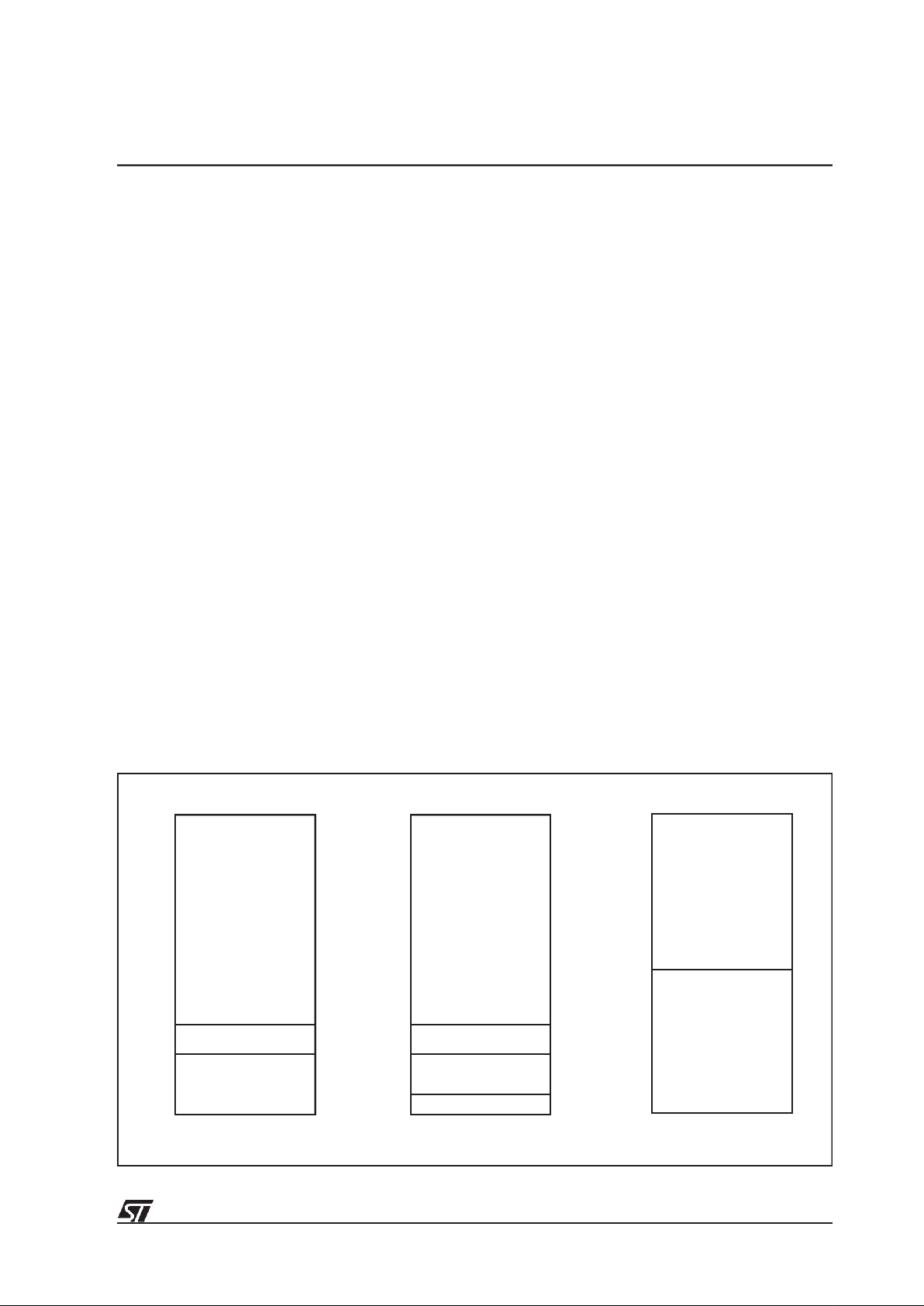
Figure 6.2 Default and user mapping examples
The BSU control registers include a reference address on bits 4 to 9, where the internal/
external memory boundary value is stored (see Figure 6.2), and software wait-states count on
bits 0 to 3, allowing up to 16 wait-states.
External addressing is recognized by comparing these address bits for each valid address
from IA, XA and YA, to the reference address contained into the corresponding control
register.
If the address is greater or equal to the reference value, an external access proceeds.
In the following register descriptions, ‘-’ means RESERVED (read: 0, write: don’t care).
EXTERNAL
INTERNAL1
64K
63K
62K
INTERNAL0
DEFAULT MAPPING (RESET)
USER MAPPING
(CAN CHANGE BY 1K STEP)
VALUE 1
VALUE 0
VALUE 1
VALUE 0
EXTERNAL
INTERNAL1
INTERNAL0
64K
0
0

20/66
ST18952
XER0/1: X-memory space control registers
After reset, XER0/1 default values are 0x83EF/0x83FF
YER0/1: Y-memory space control registers
After reset, YER0/1 default values are 0x83EF/0x83FFI
IER0/1: Instruction memory control registers
After reset, IER0/1 default values are 0x83EF/0x83FF or 0xC3EF/0xC3FF
(the EN_I value depends on the IDT_EN input value
1514131211109876543210
IM EN_X - - - - XA15 XA14 XA13 XA12 XA11 XA10 W3 W2 W1 W0
Bit Function
W3:0 Wait state count (1 to 16) for off-chip access (X-memory space)
XA15:10 X-memory space map for boundary on-chip or off-chip
EN_X Enable for X-space data exchanges
IM Intel/Motorola
0: Motorola type for memories
1: Intel type for memories (default)
15 14 13 12 11 10 9 8 7 6 5 4 3 2 1 0
IM EN_Y - - - - YA15 YA14 YA13 YA12 YA11 YA10 W3 W2 W1 W0
Bit Function
W3:0 Wait state count (1 to 16) for off-chip access (Y-memory space)
YA15:10 Y-memory space map for boundary on-chip or off-chip
EN_Y Enable for Y-space data exchanges
IM Intel/Motorola
0: Motorola type for memories
1: Intel type for memories (default)
1514131211109876543210
IM EN_I ----IA15 IA14 IA13 IA12 IA11 IA10 W3 W2 W1 W0
Bit Function
W3:0 Wait state count (1 to 16) for off-chip access (I-memory space)
IA15:10 I-memory space map for boundary on-chip or off-chip
EN_I Enable for I-space data exchanges
IM Intel/Motorola
0: Motorola type for memories
1: Intel type for memories (default)

21/66
ST18952
7 DMA Controller
The DMA controller manages data transfer between memories and external peripherals and
has the following features:
• four independent DMA channels
• transfers on X / Y / I spaces (simultaneous transfers on X and Y spaces)
• cycle stealing operation:
• 3cycles for a single data transfer (+1cycle for transfers on I space)
• (n+2) cycles for an n-data block transfer (+1cycle for transfers on I space)
• each channel has:
• 3 signals: request (DMARQ), acknowledge (DMACK), interrupt request (DIT)
• 4x16 bit registers for block transfer facilities
• fixed priority between the four channels (highest channel 0, lowest channel 3)
The DMA controller DMARQ0-3 inputs and DMACK0-3 outputs are available as primary
inputs, in the case of SIO inhibition. This is set by the DMAR register (see ”DMAR: DMA
management register” on page 44).
Figure 7.1 DMA controller
YD
YA
16
16
D950Core
INTERRUPT
CONTROLLER
PERIPHERAL
RESET
AS-DSP
HOLD
HOLDACK
INCYCLE
DMA CONTROLLER PERIPHERAL
DMARQ0
DMARQ1
DMARQ2
DMARQ3
DMACK0
DMACK1
DMACK2
DMACK3
DTACK
DIP_ENA
16 16 16 16
IA ID XA XD
IRD
IWR
IBS
XRD
XWR
XBS
YRD
YWR
YBS
DIT0 DIT1 DIT2 DIT3 DIT_AND
3
3
3
CLK
DMA_CLK
 Loading...