

SGS Thomson Microelectronics ST10R272LAT1, ST10R272L Datasheet
April 2000 1/77
This is preliminary information on a new product now in development. Details are subject to change without notice.
Rev. 1.2
■ High Performance 16-bit CPU
● CPU Frequency: 0 to 50 MHz
● 40ns instruction cycle time at 50-MHz CPU
clock
● Multiply-Accumulate unit (MAC)
● 4-stage pipeline
● Register-based design with multiple
variable register banks
● Enhanced boolean bit manip ulation
facilities
● Additional instructions to support HLL and
operating systems
● Single-cycle context switching support
● 1024 bytes on-Chip special function
register area
■ Memory Organisation
● 1KByte on-chip RAM
● Up to 16 MBytes linear address space for
code and data (1 MByte with SSP used)
■ External Memory Interface
● Programmable external bus characteristics
for different address ranges
● 8-bit or 16-bit external data bus
● Multiplexed or demultiplexed external
address/data buses
● Five programmable chip-select signals
● Hold and hold-acknowledge bus arbitration
support
■ One Channel PWM Unit
● Fail Safe Protection
● Programmable watchdog timer
● Oscillator Watchdog
■ Interrupt
● 8-channel interrupt-driven single-cycle data
transfer facilities via peripheral event
controller (PEC)
● 16-priority-level interrupt system with 17
sources, sample-rate down to 40 ns
■ Timers
● Two multi-functional general purpose timer
units with 5 timers
● Clock Generation via on-chip PLL, or via
direct or prescaled clock input
■ Serial Channels
● Synchronous/asynchronous
● High-speed-synchronous serial port SSP
■ Up to 77 general purpose I/O lines
■ No bootstrap loader
■ Electrical Characteristics
● 5V Tolerant I/Os
● 5V Fail-Safe Inputs (Port 5)
● Power: 3.3 Volt +/-0.3V
● Idle and power down modes
■ Support
● C-compilers, macro-assembler packages,
emulators, evaluation boards, HLLdebuggers, simulators, logic analyser
disassemblers, programming boards
■ Package
● 100-Pin Thin Quad Flat Pack (TQFP)
ST10 CORE
DPRAM
Interrupt Controller
P.4
P.1 P.0
Po.2
P.6
P.3
Dedicated
pins
ASC GPT1/2
&PEC
WDT
XSSP
P.5
OSC
PLL
P.7
PWM
MAC
ST10R272L
16-BIT LOW VOLTAGE RO MLESS MCU WITH MAC
PRODUCT PREVIEW
1

2/77
Table of Contents
77
1
1 PIN DESCRIPTIO N . . . . . . . . . . . . . . . . . . . . . . . . . . . . . . . . . . . . . . . . . . . . . . . . . . . . 4
2 FUNCTIONAL DESCRIPTION . . . . . . . . . . . . . . . . . . . . . . . . . . . . . . . . . . . . . . . . . . 11
3 MEMORY MAPPING . . . . . . . . . . . . . . . . . . . . . . . . . . . . . . . . . . . . . . . . . . . . . . . . . 12
4 CENTRAL PROCESSING UNIT . . . . . . . . . . . . . . . . . . . . . . . . . . . . . . . . . . . . . . . . . 13
5 MULTIPLY-ACCUMULATE UNIT (MAC) . . . . . . . . . . . . . . . . . . . . . . . . . . . . . . . . . . 14
5.1 MAC FEATURES . . . . . . . . . . . . . . . . . . . . . . . . . . . . . . . . . . . . . . . . . . . . . . . 15
5.2 MAC OPERATION . . . . . . . . . . . . . . . . . . . . . . . . . . . . . . . . . . . . . . . . . . . . . . 16
6 INTERRUPT AND TRAP FUNCTIONS . . . . . . . . . . . . . . . . . . . . . . . . . . . . . . . . . . . 22
6.1 INTERRUPT SOURCES . . . . . . . . . . . . . . . . . . . . . . . . . . . . . . . . . . . . . . . . . . 23
6.2 HARDWARE TRAPS . . . . . . . . . . . . . . . . . . . . . . . . . . . . . . . . . . . . . . . . . . . . 24
7 PARALLEL P ORTS . . . . . . . . . . . . . . . . . . . . . . . . . . . . . . . . . . . . . . . . . . . . . . . . . . 25
8 EXTERNAL BUS CONTROLLER . . . . . . . . . . . . . . . . . . . . . . . . . . . . . . . . . . . . . . . 25
9 PWM MODUL E . . . . . . . . . . . . . . . . . . . . . . . . . . . . . . . . . . . . . . . . . . . . . . . . . . . . . . 26
10 GENERAL PU RPOSE TIMERS . . . . . . . . . . . . . . . . . . . . . . . . . . . . . . . . . . . . . . . . 27
10.1 GPT1 . . . . . . . . . . . . . . . . . . . . . . . . . . . . . . . . . . . . . . . . . . . . . . . . . . . . . . . . . 27
10.2 GPT2 . . . . . . . . . . . . . . . . . . . . . . . . . . . . . . . . . . . . . . . . . . . . . . . . . . . . . . . . . 29
11 SERIAL CHANNELS . . . . . . . . . . . . . . . . . . . . . . . . . . . . . . . . . . . . . . . . . . . . . . . . 30
12 WATCHDOG TIMER . . . . . . . . . . . . . . . . . . . . . . . . . . . . . . . . . . . . . . . . . . . . . . . . . 32
13 SYSTEM RESET . . . . . . . . . . . . . . . . . . . . . . . . . . . . . . . . . . . . . . . . . . . . . . . . . . . . 33
14 POWER REDUCTION MODES . . . . . . . . . . . . . . . . . . . . . . . . . . . . . . . . . . . . . . . . 34
15 SPECIAL FUNCTION REGISTERS . . . . . . . . . . . . . . . . . . . . . . . . . . . . . . . . . . . . . 34
16 ELECTRICAL CHARACTERISTICS . . . . . . . . . . . . . . . . . . . . . . . . . . . . . . . . . . . . 40
16.1 ABSOLUTE MAXIMUM RAT INGS . . . . . . . . . . . . . . . . . . . . . . . . . . . . . . . . . . 40
16.2 DC CHARACTERISTICS . . . . . . . . . . . . . . . . . . . . . . . . . . . . . . . . . . . . . . . . . 42
16.3 AC CHARACTERISTICS . . . . . . . . . . . . . . . . . . . . . . . . . . . . . . . . . . . . . . . . . 45

3/77
Table of Contents
16.3.1 CPU clock generation mechanisms . . . . . . . . . . . . . . . . . . . . . . . . . . . . . . . . . . . . 47
16.3.2 Memory cycle variables . . . . . . . . . . . . . . . . . . . . . . . . . . . . . . . . . . . . . . . . . . . . . . 51
16.3.3 Multiplexed bus . . . . . . . . . . . . . . . . . . . . . . . . . . . . . . . . . . . . . . . . . . . . . . . . . . . . 52
16.3.4 Demultiplexed bus . . . . . . . . . . . . . . . . . . . . . . . . . . . . . . . . . . . . . . . . . . . . . . . . . 59
16.3.5 CLKOUT and READY
/READY . . . . . . . . . . . . . . . . . . . . . . . . . . . . . . . . . . . . . . . . 66
16.3.6 External bus arbitration . . . . . . . . . . . . . . . . . . . . . . . . . . . . . . . . . . . . . . . . . . . . . . 69
16.3.7 External hardware reset . . . . . . . . . . . . . . . . . . . . . . . . . . . . . . . . . . . . . . . . . . . . . 72
16.3.8 Syn chronous serial port timing . . . . . . . . . . . . . . . . . . . . . . . . . . . . . . . . . . . . . . . . 75
17 PACKAGE MECHANICAL DAT A . . . . . . . . . . . . . . . . . . . . . . . . . . . . . . . . . . . . . . 77
18 ORDERING IN FORMATION . . . . . . . . . . . . . . . . . . . . . . . . . . . . . . . . . . . . . . . . . . . 77
4/77
ST10R272L - PIN DESCRIPTION
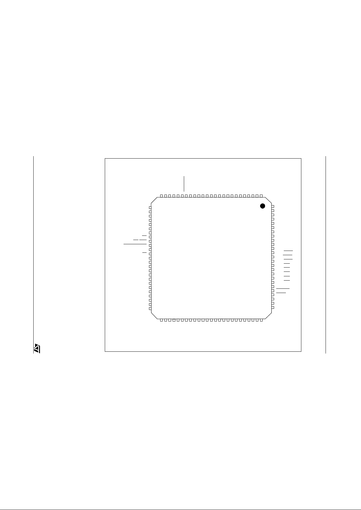
1 PIN DESCRIPTION
Figure 1 TQFP-100 pin configuration (top view)
12345678910111213141516171819202122232425
26
272829303132 33 34 35 36 37 38 39 40414243444546 47 48 49 50
75747372717069686766656463626160595857565554535251
100999897969594939291908988878685848382818079787776
P5 .1 3/T5IN
P5.14/T4EUD
P5.15/T2EUD
V
SS
XTAL1
XTAL2
V
DD
P3.0
P3 .1 /T6OU T
P3.2/CAPIN
P3 .3 /T3OU T
P3 .4 /T3EU D
P3 .5 /T 4IN
P3 .6 /T 3IN
P3 .7 /T 2IN
P3.8
P3.9
P3.10/TxD0
P3.11/RxD0
P3.12/BHE/WRH
P3.13
P3.15/CLKOUT
P4 .0 /A16
P4 .1 /A17
P4 .2 /A18
P1H.6/A14
P1H.5/A13
P1H.4/A12
P1H.3/A11
P1H.2/A10
V
SSVDD
P1H.1/A9
P1H.0/A8
P1L.7/A7
P1L.6/A6
P1L.5/A5
P1L.4/A4
P1L.3/A3
P1L.2/A2
P1L.1/A1
P1L.0/A0
P0H.7/AD15
P0H.6/AD14
P0H.5/AD13
P0H.4/AD12
P0H.3/AD11
P0H.2/AD10
P0H.1/AD9
P0H.0/AD8
P5.12/T6IN
P5.11/T5EUD
P5.10/T6EUD
P7.3/POUT3
P7.2
P7.1
P7.0
P2.11/EX3IN
P2.10/EX2IN
P2.9/EX1IN
P2.8/EX0IN
P6.7/BREQ
P6.6/HLDA
P6.5/HOLD
P6.4/CS4
P6.3/CS3
P6.2/CS2
P6.1/CS1
P6.0/CS0
NMI
RSTOUT
RSTIN
V
DD
V
SS
P1H.7/A15
P4.3/A19
V
SS
V
DD
P4.4/A20/SSPCE1
P4.5/A21/SSPCE0
P4.6/A22/SSPDAT
P4.7/A23/SSPCLK
RD
WR/WRL
READY/READY
ALE
EA
V
DD
V
SS
RPD
P0L.0/AD0
P0L.1/AD1
P0L.2/AD2
P0L.3/AD3
P0L.4/AD4
P0L.5/AD5
P0L.6/AD6
P0L.7/AD7
V
DD
V
SS
ST10R 272L
1

5/77
ST10R272L - PIN DESCR IPTION
Symbol
Pin Number
(TQFP)
Input (I)
Output (O)
Kind
1)
Function
P5.10
–P5.15
98-100
1- 3
I
I
5S5S6-bit input-only port with Schmitt-Trigger characteristics.
Port 5 pins also serve as timer inputs:
98 I 5S P5.10 T6EUD GPT2 Timer T6 Ext.Up/Down
Ctrl.Input
99 I 5S P5.11 T5EUD GPT2 Timer T5 Ext.Up/Down
Ctrl.Input
100 I 5S P5.12 T6IN GPT2 Timer T6 Count Input
1 I 5S P5.13 T5IN GPT2 Timer T5 Count Input
2 I 5S P5.1 4 T4 EUD GPT1 Timer T4 Ex t. Up / Down
Ctrl.Input
3 I 5S P5.1 5 T2 EUD GPT1 Timer T2 Ex t. Up / Down
Ctrl.Input
XTAL1
XTAL2
5 I 3T X TAL1: Input to the oscillator amplifier and internal clock
generator
6 O 3T XTAL2: Output of the oscillator amplifier circuit.
To clock the device from an external source, drive
XTAL1, while leaving XTAL2 unconnected.
Observe minimum and maximum high/low and
rise/fall times specified in the AC Characteristics.
Table 1 Pin definiti ons
1
6/77
ST10R272L - PIN DESCR IPTION
P3.0 –
P3.13
P3.15
8-21
22
I/O
I/O
5T 5TA 15-bit (P3.14 is missing) bidirectional I/O port. Port 3 is bit-
wise programmable for input or output via direction bits. For a
pin configured as input, the output driver is put into highimpedance state. Port 3 outputs can be configured as push/
pull or open drain drivers. The following pins have alternate
functions:
9 O 5T P3.1 T6OUT GPT2 Timer T6 toggle latch output
10 I 5T P3. 2 CAPIN GPT2 Register CAPREL capture
input
11 O 5T P3.3 T3OUT GPT1 Timer T3 toggle latch output
12 I 5T P3. 4 T3EUD GPT1 Timer T3 ext.up/down ctrl.input
13 I 5T P3. 5 T4IN GPT1 Timer T4 input for count/gate/
reload/capture
14 I 5T P 3.6 T3IN GPT1 Timer T3 count/ gate input
15 I 5T P3. 7 T2IN GPT1 Timer T2 input for count/gate/
reload/capture
18 O 5T P3.10 TxD0 ASC0 clock/data output (asyn./syn.)
19 I/O 5T P3. 11 RxD0 ASC0 data input (asyn.) or I/O (syn.)
20 O 5T P3.12 BHE
Ext. Memory High Byte Enable Signal
O5T WRH
Ext. Memory High Byte Write Strobe
22 O 5T P3.15 CLKOUT System clock output (=CPU clock)
Symbol
Pin Number
(TQFP)
Input (I)
Output (O)
Kind
1)
Function
Table 1 Pin definiti ons
1
7/77
ST10R272L - PIN DESCR IPTION
P4.0–
P4.7
23-26
29-32-
I/O 5T An 8-bit bidirectional I/O port. Port 8 is bit-wise programmable
for input or output via direction bits. For a pin configured as
input, the output driver is put into high-impedance state.
Port 4 can be used to output the segment address lines for
external bus configuration.
23 O 5T P4.0 A16 Least Significant Segment Addr. Line
... ... ... ... ... ...
26 O 5T P4.3 A19 Segment Address Line
29 O 5T P4.4 A20 Segment Address Line
O 5T SSPCE1 Chip Enable Line 1
30 O 5T P4.5 A21 Segment Address Line
O 5T SSPCE0 SSPChip Enable Line 0
31 O 5T P4.6 A22 Segment Address Line
I/O 5T SSPDAT SSP Data Input/Outpu t Line
32 O 5T P4.7 A23 Most Significant Segment Addr. Line
O 5T SSPCLK S SP Clock Output Line
RD
33 O 5T External Memory Read Strobe. RD is activated for every exter-
nal instruction or data read access.
WR/
WRL
34 O 5T External Memory Write Strobe. In WR-mode, this pin is acti-
vated for every external data write access. In WRL-mode, this
pin is activated for low byte data write accesses on a 16-bit
bus, and for every data write access on an 8-bit bus.
See WRCFG in the SYSCON register for mode selection.
READY/
READY
35 I 5T Ready Input. Active level is programmable. When the Ready
function is enabled, the selected inactive level at this pin dur-
ing an external memory access will f orce t he insertion of mem-
ory cycle time waitstates until the pin returns to the selected
active level. Polarity is pro gram mable.
Symbol
Pin Number
(TQFP)
Input (I)
Output (O)
Kind
1)
Function
Table 1 Pin definiti ons
1
8/77
ST10R272L - PIN DESCR IPTION
ALE 36 O 5T Address Latch Enable Output. Can be used for latching the
address into external memory or an address latch in the multi-
plexed bus modes.
EA
37 I 5T E xt ernal Access Enable pin. Low level at this pin during and
after reset forces the ST10R272L to begin instruction execu-
tion out of external memory. A high level forces execution out
of the internal ROM. The ST10R272L must have this pin tied
to ‘0’.
PORT0:
P0L.0–
P0L.7,
P0H.0 -
P0H.7
41 - 48
51 - 58
I/O 5T PORT0 has two 8-bit bidirectional I/O ports P0L and P0H. It is
bit-wise programmable for input or output via direction bits. For
a pin configured as input, the output driver is put into high-
impedance state.
For external bus configuration, PORT0 acts as address (A)
and address/data (AD) bus in multiplexed bus modes and as
the data (D) bus in demultiplexed bus modes.
PORT1:
P1L.0–
P1L.7,
P1H.0 -
P1H.7
59- 66
67, 68
71-76
I/O 5T PORT1 has two 8-bit bidirectional I/O ports P1L and P1H. It is
bit-wise programmable for input or output via direction bits. For
a pin configured as input, the output driver is put into high-
impedance state. PORT1 acts as a 16-bit address bus (A) in
demultiplexed bus modes and also after switching from a
demultiplexed bus mode to a multiplexed bus mode.
Symbol
Pin Number
(TQFP)
Input (I)
Output (O)
Kind
1)
Function
Table 1 Pin definiti ons
Demultiplexed bus modes
Data Path Width: 8-bit 16-bit
P0L.0 – P0L.7: D0 – D7 D0 - D7
P0H.0 – P0H.7: I/O D8 - D15
Multiplexed bus modes
Data Path Width: 8-bit 16-bit
P0L.0 – P0L.7: AD0 – AD7 AD0 - AD7
P0H.0 – P0H.7: A8 – A15 AD8 – AD15
1
9/77
ST10R272L - PIN DESCR IPTION
RSTIN 79 I 5T Reset Input with Schmitt-Tr ig ger characteristics. Resets the
device when a low level is applied for a specified duration while
the oscillator is running. An internal pullup resi stor enables
power-on reset using only a capacitor connected to
V
SS
. With
a bonding option, the RSTIN
pin can also be pulled-down for
512 internal clock cycles for hardware, software or watchdog
timer triggered resets
RSTOUT
80 O 5T Internal Reset Indication Output. This pin is set to a low level
when the part is executes hardware-, software- or watchdog
timer reset. RSTOUT
remains low until the EINIT (end of ini-
tialization) instruction is executed.
NMI
81 I 5S Non-Maskable Interrupt Input. A high to low transition at this
pin causes the CPU to vector to the NMI trap routine.
If it is not used, NMI
should be pulled high externally.
P6.0P6.7
82-89 I/O 5T An 8-bit bidirectional I/O port. Port 6 is bit-wise programmable
for input or output via direction bits. For a pin configured as
input, the output driver is put into high-impedance state. Port 6
outputs can be configured as push/pull or open drain drivers.
The following Port 6 pins have alternate functions:
82 O 5T P6.0 CS0
Chip Select 0 Output
... ... ... ... ... ...
86 O 5T P6.4 CS4
Chip Select 4 Output
87 I 5T P 6. 5 HOL D
External Master Hold Request Input
(Master mode: O, Slave mode: I)
88 I/O 5T P6.6 HLDA
Hold Acknowledge Output
89 O 5T P6.7 BRE Q
Bus Request Output
Symbol
Pin Number
(TQFP)
Input (I)
Output (O)
Kind
1)
Function
Table 1 Pin definiti ons
1
10/77
ST10R272L - PIN DESCR IPTION
P2.8 –
P2.11
90 - 93 I/O 5T Por t 2 is a 4-bit bidirectional I/O port. It is bit-wise programma-
ble for input or output via di rection bits. For a pin configured as
input, the output driver is put into high-impedance state. Port 2
outputs can be configured as push/pull or open drain drivers.
The following Port 2 pins have alternate functions:
90 I 5T P 2.8 EX0IN Fast External Interrupt 0 Input
... ... ... ... ... ...
93 I 5T P 2.11 EX 3IN Fast External Interrupt 3 Input
P7.0 –
P7.3
94 - 97 I/O 5T Por t 7 is a 4-bit bidirectional I/O port. It is bit-wise programma-
ble for input or output via di rection bits. For a pin configured as
input, the output driver is put into high-impedance state. Port
7outputs can be configured as push/pull or open drain drivers.
The following Port 7 pins have alternate functions:
97 O 5T P7.3 POUT3 PWM (Channel 3) Output
RPD 40 I/O 5T Input timing pin for the return from powerdown circuit and
power-up asynchronous reset.
V
DD
7, 28,
38, 49,
69, 78
- PO Digital supply voltage.
V
SS
4, 27,
39, 50,
70, 77
- PO Digital ground.
1) The following I/O kinds are used. Refer to
ELECTRICAL CHARACTERISTICS
on
page 40 for a detailed description.
PO: Power pin
3T: 3 V tolerant pin (voltage max. respect to Vss is -0.5 to VDD + 0.5)
5V: 5 V tolerant pin (voltage max. respect to Vss is -0.5 to 5.5 only if chip is powered)
5S: 5 V tolerant and f ail-safe pin (-0.5-5.5 ma x. voltage w.r.t. Vss ev en if chip is n ot pow-
ered).
Symbol
Pin Number
(TQFP)
Input (I)
Output (O)
Kind
1)
Function
Table 1 Pin definiti ons
1
11/77
ST10R272L - FUNCTIONAL DESCRIPTION
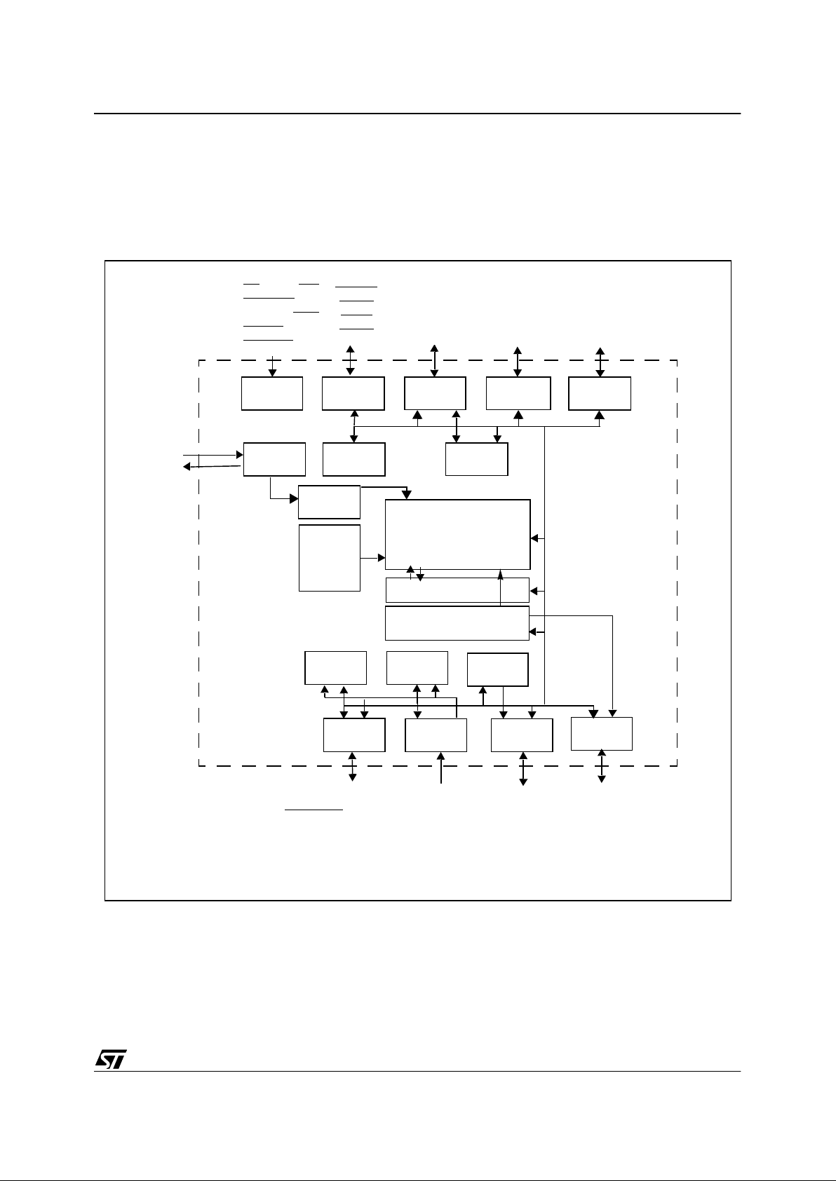
2 FUNCTI ONAL DESCRIPTION
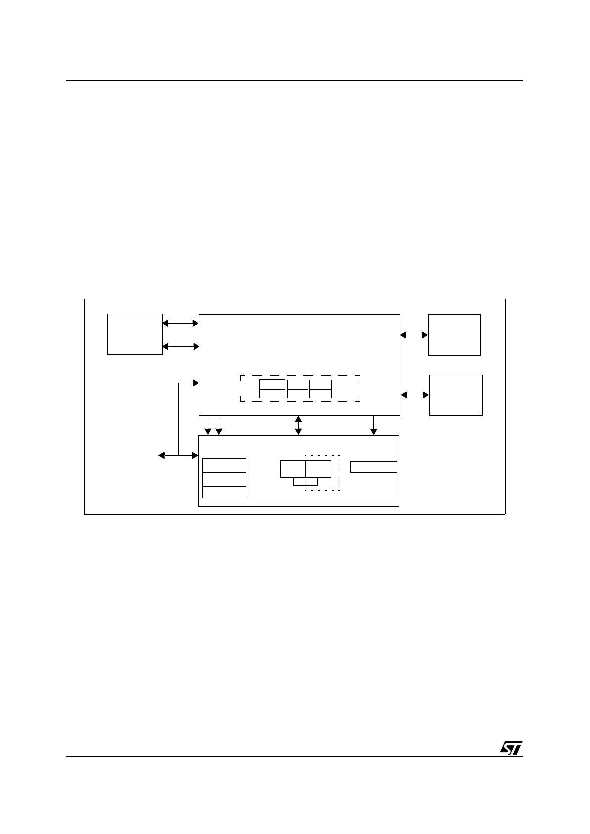
ST10R272L architecture combines the advantages of both RISC and CISC processors wi th
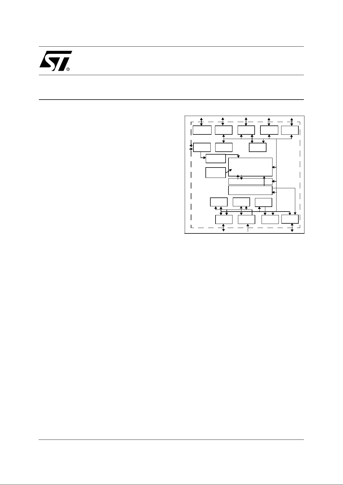
an advanced peripheral subsystem. The following block diagram overviews the different onchip components and the internal bus structure.
Figure 2 Block diagram
ST10 CO RE
1KByte
DPRAM
Interrupt Controller
Port 4
Port 1
8-bit
2x8-bit
Port 0
2x8-bit
Port 2
4-bit
Port 6
8-bit
I/O
CS(4:0)
I/O
HOLD
HLDA
BREQ
A(15:0)
I/O, D(7:0)
D(15:8), D(7:0)
A(15:8), AD(7:0)
AD(15:8), AD(7:0)
I/O
Port 3
15-bit
I/O
EXIN(3:0)
XTAL1
dedicated
pins
ASC GPT1/2
&
PEC
I/O
CLKOUT,
BHE/WRH
, RxD0,
TxD0, T2IN, T3IN,
T4IN, T3EUD,
T3OUT, CAPIN,
T6OUT
I
T2EUD,
T4EUD, T5IN,
T6IN, T5EUD,
T6EUD
EA, ALE, RD,
WR/WRL,
READY, NMI,
RSTIN,
RSTOUT
WDT
XSSP
4-bit
I/O
A(23:16),
SSPCLK,
SSPDAT,
SSPCE(1:0)
Port 5
6-bit
OSC
PLL
XTAL2
Port 7
4-bit
PWM
I/O
POUT3
MAC
1
12/77
ST10R272L - MEMORY MA PPING
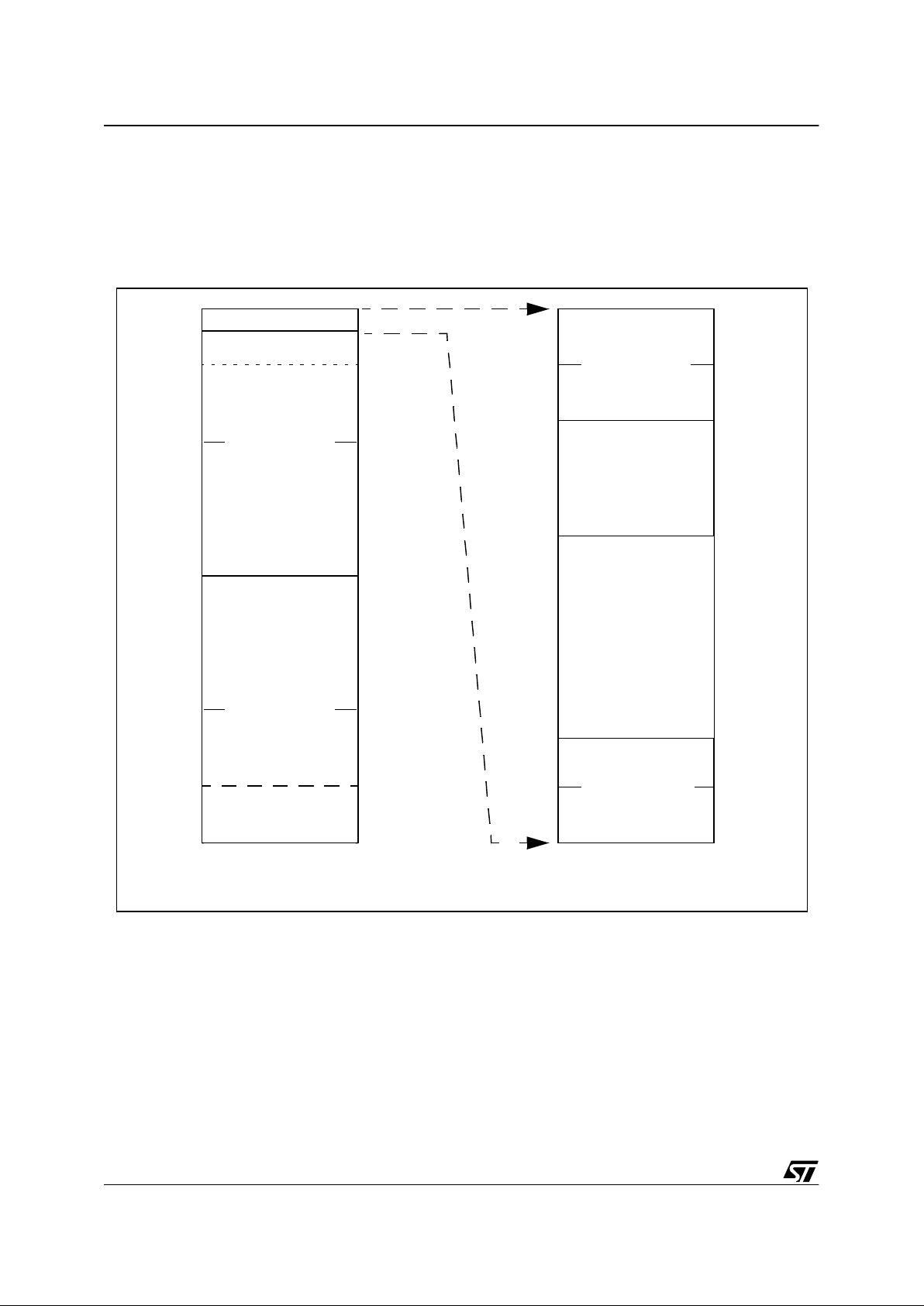
3 MEMORY MAPPING
The ST10R272L is a ROMless device, the internal RAM space is 1 KByte. The RAM address
space is used for variables, register banks, the system stack, the PEC pointers (in 00’FCE0h
- 00’FCFFh) and the bit-addressable space (in 00’FD00h - 00’FDFFh).
Figure 3 Memory map
XSSP
Data Page 0
Data Page 1
Data Page 2
Data Page 3
00’0000h
00’4000h
00’8000h
00’F000h
00’F000h
00’FFFFh
00’0000h
00’1FFFh
8K-byte
00’EF00h
00’EFFFh
256 Byte
internal
memory
00’F000h
00’F200h
00’FE00h
00’FFFFh
SFR Area
(reserved)
1K-Byte
RAM/SFR
DPRAM / SFR Area
4 K-Byte
System Segment 0
64 K-Byte
External
memory
00’FE20h
00’FE3Fh
00’FF20h
00’FF3Fh
ESFR Area
(reserved)
00’F020h
00’F03Fh
00’FF20h
00’FF3Fh
RAM
00’FA00h
Block 1
Block 0
1
13/77
ST10R272L - CENTRAL PROCESSING UNIT
4 CENTRAL PROCESSING UNIT
The main core of the CPU contains a 4-stage instruction pipeline, a MAC multiplyaccumulation unit, a separate multiply and divide unit, a bit-mask generator and a barrel
shifter. Most instructions can be ex ecuted i n one machine cycle r equiring 40ns at 50MHz CPU
clock.
The CPU includes an actual register context consisting of 16 wordwide GPRs physically
located in the on-chip RAM area. A Context Pointer (CP) register determines the base
address of the activ e register bank to be ac cessed b y the CPU . T he number of r egister banks
is only restricted by the available internal RAM space. For easy parameter passing, one
register bank may overlap others.
A system stack of up to 1024 bytes is provided as a storage for temporary data. The system
stack is al located in the on-chip RAM area, and it i s accessed by the C PU via the stac k pointer
(SP) register. Two separate SFRs, STKOV and STKUN, are compared against the stack
pointer value during each stack access to detect stack overflow or underflow.
Figure 4 CPU block diagram
16
16
Internal
RAM
1KByte
R15
R0
General
Purpose
Registers
R0
R15
MDH
MDL
Barrel-Shift
Mul./Div.-HW
Bit-Mask Gen.
ALU
16-Bit
Context Ptr
ADDRSEL 1
ADDRSEL 2
ADDRSEL 3
ADDRSEL 4
Code Seg. Ptr.
CPU
IDX0
IDX1
QX1
QX0
QR0
QR1
SP
STKOV
STKUN
Exec. Unit
Instr. Ptr
Instr. Reg
4-Stage
Pipeline
PSW
SYSCON
BUSCON 0
BUSCON 1
BUSCON 2
BUSCON 3
BUSCON 4
Data Pg. Ptrs
1
14/77
ST10R272L - MULTIPLY-ACCUMULATE UNIT (MAC)
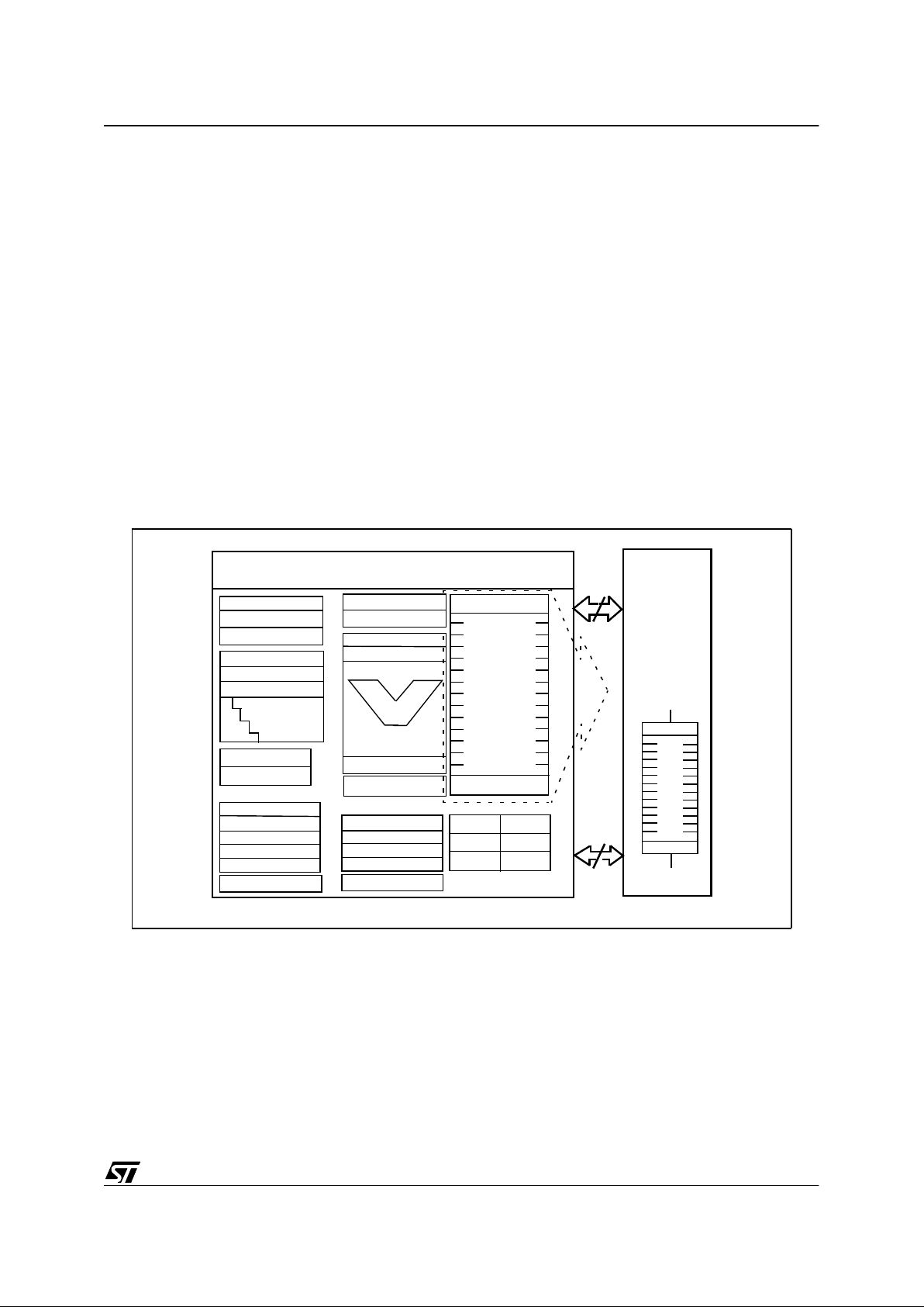
5 MULTIPLY-ACCUMULATE UNIT (MAC)
The MAC is a specialized co-processor added to the ST10R272L CPU core to improve the
performance of signal processing algorithms. It includes:
• a multiply-accumulate unit
• an address generation unit, able to feed the mac unit with 2 operands per cycle
• a repeat unit, to execute a series of multiply-accumulate instructions
New addressing capabilities enable the CPU to supply the MAC with up to 2 operands per
instruction cycle. MAC instructions: multiply, multiply-accumulate, 32-bit signed arithmetic
operations and the CoMOV transfer ins tru ction have been added to the standard instruction
set. Full details are provided in the ‘ST10 Family Programming Manual’.
Figure 5 MAC architecture
MAC CoProcessor
dual-port
internal RAM
external
memory
memory
program
new addressing features
IDX0
IDX1
QX0
QX1
QR0
QR1
operands
control
program code
data buses
16 x16
multiplier
40-bit ALU
shifter
MCW
MAL
MRW MAH
MSW
repeat unit
40-bit accumulator
Peripheral
interface
ST10R272L CPU
1

15/77
ST10R272L - MULTIPLY-ACCU MULATE UNIT (MAC)
5.1 MAC Features
Enhanced addressing capabilities
•
Double indirect addressing mode with pointer post-modification.
• Parallel Data Move allows one operand move during Multiply-Accumulate instructions
without penalty.
• CoSTORE instruction (for fast access to the MAC SFRs) and CoMOV (for fast memory to
memory table transfer).
General
•
Two-cycle execution for all MAC operations.
• 16 x 16 signed/unsigned parallel multiplier.
• 40-bit signed arithmetic unit with automatic saturation mode.
• 40-bit accumulator.
• 8-bit left/right shifter.
• Scaler (one-bit left shifter)
• Data limiter
• Full instruction set with multiply and multiply-accumulate, 32-bit signed arithmetic and
compare instructions.
• Three 16-bit status and control registers: MSW: MAC Status Word, MCW: MAC Control
Word, MRW: MAC Repeat Word.
Progra m control
•
Repeat Unit allows some MAC co-pr ocessor instructions to be repeated up to 8192 times .
Repeated instructions may be interrupted.
• MAC interrupt (Class B Trap) on MAC condition flags.
1

16/77
ST10R272L - MULTIPLY-ACCUMULATE UNIT (MAC)
5.2 MAC Operation
Instruction pipelini ng
All MAC instructions use the 4-stage pipeline. During each stage the following tasks are
performed:
• FETCH: All new instructions are double-word instructions.
• DECODE: If required, operand addresses are calculated and the resulting operands are
fetched. IDX and GPR pointers are post-modified if necessary.
• EXECUTE: Performs the MAC operation. At the end of the cycle, the Accumulator and the
MAC condition flags are updated if required. Modified GPR pointers are written-back
during this stage, if required.
• WRITEBACK: Operand write-back in the case of parallel data move.
Note At least one instruction which does not use the MAC must be inserted between two
instructions that read from a MAC register. This is because the Accumulator and the
status of the MAC are modified during the Execute stage. The CoSTORE instruction
has been added to allow access to the MAC registers immediately after a MAC
operation.
Address generation
MAC instructions can use some standard ST10 addressing modes such as GPR direct or
#data4 for immediate shift value.
New addressing modes have been added to supply the MAC with two new operands per
instruction cycle. These allow indirect addressing with address pointer post-modification.
Double indirect addressing requires two pointers. Any GPR can be used for one pointer, the
other pointer is provided by one of two specific SFRs IDX0 and IDX1. Two pairs of offset
registers QR0/QR1 and QX0/QX1 are associated with each pointer (GPR or IDX
i
). The GPR
pointer allows access to the entire memory space, but IDX
i
are limited to the internal Dual-
Port RAM, except for the CoMOV instruction.
1
17/77
ST10R272L - MULTIPLY-ACCU MULATE UNIT (MAC)
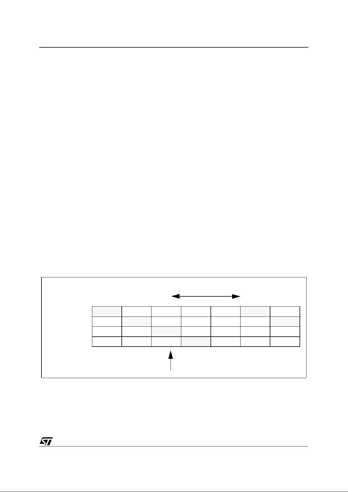
The following table shows the various combinations of pointer post-modification for each of
these 2 new addressing modes. In this document the symbols “[Rw
n
⊗]” and “[IDXi⊗]” refer to
these addressing modes.
For the CoMACM class of instruction, Parallel Data Move mechanism is implemented. This
class of instruction is only a vailable with double indirect addres sing mode. P ar al lel D ata Mo v e
allows the operand pointed by IDX
i
to be moved to a new location in parallel with the MAC
operation. The write-back address of Parallel Data Move is calculated depending on the postmodification of IDX
i
. It is obtained by the rev erse oper ation than the one used to calculate the
new value of IDX
i
. The following table shows these rules.
Symbol Mnemonic Address Pointer Operation
“[IDXi⊗]” stands for [IDXi](IDX
i
) ← (IDXi) (no-op)
[IDXi+](IDX
i
) ← (IDXi) +2 (i=0,1)
[IDXi -] (IDXi) ← (IDXi) -2 (i=0,1)
[IDXi + QXj](IDX
i
) ← (IDXi) + (QXj) (i, j =0,1)
[IDXi - QXj](IDX
i
) ← (IDXi) - (QXj) (i, j =0,1)
“[Rw
n
⊗]” stands for [Rwn] (Rwn) ← (Rwn) (no-op)
[Rwn+] (Rwn) ← (Rwn) +2 (n=0-15)
[Rwn-] (Rwn) ← (Rwn) -2 (k=0-15)
[Rwn+QRj] (Rwn) ← (Rwn) + (QRj) (n=0-15;j =0,1)
[Rwn - QRj] (Rwn ) ← (Rwn) - (QRj) (n=0-15; j =0,1)
Table 2 Pointer post-modification combinations for IDXi and Rwn
Instructio n Writeback Address
CoMACM [IDX
i
+],... <IDXi-2>
CoMACM [IDX
i
-],... <IDXi+2>
CoMACM [IDX
i
+QXj],... <IDXi-QXj>
CoMACM [IDX
i
-QXj],... <IDXi+QXj>
Table 3 Parallel data move addressing
1
18/77
ST10R272L - MULTIPLY-ACCUMULATE UNIT (MAC)
The Parallel Data Move shifts a table of operands in parallel with a computation on those
operands. Its specific use is for signal processing algorithms like filter computation. The
following figure gives an example of Parallel Data Move with CoMACM instruction.
16 x 16 signed/unsigned parallel mul tiplier
The multiplier executes 16 x 16-bit parallel signed/unsigned fractional and integer multiplies.
The multiplier has two 16-bit i nput ports, and a 32-bit product output port. The input ports can
accept data from the MA-bus and from the MB-bus. The output is sign-extended and then
feeds a scaler that shifts the multiplier output according to the shift mode bit MP specified in
the co-processor Control Word (MCW). The product can be shifted one bit left to compensate
for the extra sign bit gained in multiplying two 16-bit signed (2’s complement) fractional
numbers if bit MP is set.
40-bit signed arithmetic unit
The arithmetic unit over 32 bits wide to allow intermediate overflow in a series of multiply/
accumulate operations. The extension flag E, contained in the most significant byte of MSW,
is set when the Accumulator has overflowed beyond the 32-bit boundary, that is, when there
are significant (non-sign) bits in the top eight (signed arithmetic) bits of the Accumulator.
The 40-bit arithmetic unit has two 40-bit input ports A and B. The A-input port accepts data
from 4 possible sources: 00,0000,0000h, 00,0000,8000h (round), the sign-extended product,
or the sign-extended data c on veyed b y the 32-bit b us result ing from the concatenation of MAand MB-buses. Product and Concatenation can be shifted left by one according to MP for the
multiplier or to the i ns truction f or the concatenation. The B-input port is fed either by the 40-bit
shifted/not shifted and inverted/not inverted accumulator or by 00,0000,0000h. A-input and B-
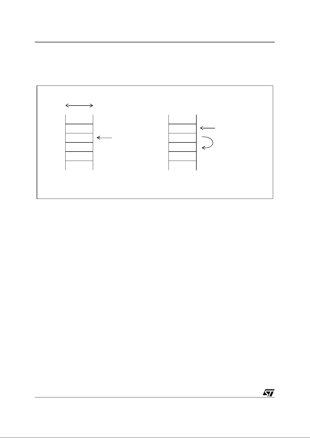
Figure 6 Example of parallel data move
CoMACM [IDX0+], [R2+]
X
n+2
n
n-2
n-4
16-bit
IDX0 X
X
n+2
n
n-2
n-4
IDX0
Parallel Data Move
After ExecutionBefore Execution
1

19/77
ST10R272L - MULTIPLY-ACCU MULATE UNIT (MAC)
input ports can receive 00,0000,0000h to allow direct transfers from the B-source and Asource, respectively, to the Accumulator (case of Multiplication, Shift.). The output of the
arithmetic unit goes to the Accumulator.
It is also possible to saturate the Accumulator on a 32-bit value, automatically after every
accumulation. Automatic saturation is enabled by setting the saturation bit MS in the MCW
register. When the Accumulator is in the saturation mode and an 32-bit overflow occurs, the
accumulator is loaded with either the most positive or the most negative value representable
in a 32-bit value, depending on the direction of the overflow. The value of the Accumulator
upon saturation is 00,7fff,ffffh (positive) or ff,8000,0000h (negative) in signed arithmetic.
Automatic saturation sets the SL flag MSW. This flag is a sticky flag which means it stays set
until it is explicitly reset by the user.
40-bit overflow of the Accumulator sets the SV flag in MSW. This flag is also a sticky flag.
40-bit accumulator register
The 40-bit Accumulator consists of three SFR registers MAH, MAL and MAE. MAH and MAL
are 16-bit wide. MAE is 8-bit wide and is contained within the least significant byte of MSW.
Most co-processor operations specify the 40-bit Accumulator register as source and/or
destination operand.
Data limite r
Saturation arithmetic is also provided to selectively limit overflow, when reading the
accumulator by means of a CoSTORE <destination>
MAS instruction. Limiting is performed
on the MAC Accumulator. If the contents of the Accumulator can be represented in the
destination operand size without overflow, the data limiter is disabled and the operand is not
modified. If the contents of the accumulator cannot be represented without overflow in the
destination operand size, the limiter will substitute a ‘limited’ data as explained in the f ollowing
table.
Note In this case, the accumulator and the status register are not affected. MAS readable
from a CoSTORE instruction.
Register E bit N bit Output of the Limiter
x 0 x unchanged
MAS 1 0 7fffh
MAS 1 1 8000h
Table 4 Data Limit Values
1

20/77
ST10R272L - MULTIPLY-ACCUMULATE UNIT (MAC)
Accumulator shi fter
The Accumulator shifter is a parallel shifter with a 40-bit input and a 40-bit output. The source
operand of the shifter is the Accumulator and the possible shifting operations are:
• No shift (Unmodified)
• Up to 8-bit Arithmetic Left Shift
• Up to 8-bit Arithmetic Right Shift
E, SV and SL bits from MSW are affected by Left shifts, theref or e i f the s atur ation mechanism
is enabled (MS), the behavior is similar to the one of the arithmetic unit. The carry flag C is
also affected by left shifts.
Repeat unit
The MAC includes a repeat unit allowing the repetition of some co-processor instructions up
to 2
13
(8192) times. The repeat count may be specified either by an immediate value (up to 31
times) or by the content of the Repeat Count ( bits 12 to 0) i n the MAC Repeat Word (MRW). If
the Repeat Count equals “N” the instruction will be executed “N+1” times. At each iteration of
a cumulative instruction the Repeat Count is tested for zero. If it is zero the instruction is
terminated else the Repeat Count is decremented and the instruction is repeated. During
such a repeat sequence, the Repeat Flag in MRW is set until the last execution of the
repeated instruction.
The syntax of repeated instructions is shown in the following examples:
In example 1, the instruction is repeated according to a 5-bit immediate value. The Repeat
Count in MRW is automatically loaded with this value minus one (MRW=23).
In this example, the instruction is repeated according to the Repeat Count in MRW . Notice that
due to the pipeline processing at least one instruction should be inserted between the write of
MRW and the next repeated instruction.
Repeat sequences may be interrupted. When an interrupt occurs during a repeat sequence,
the sequence is stopped and the i nterrupt routine i s e xecuted. The repeat sequence resumes
at the end of the interrupt routine. During the interrupt, MR remains set, indicating that a
repeated instruction has been interrupted and the Repeat Count holds the number (minus 1)
1 Repeat #24 times
CoMAC[IDX0+],[R0+] ; repeated 24 times
1 MOV MRW, #00FFh ; load MRW
NOP ; instruction latency
Repeat MRW times
CoMACM [IDX1-],[R2+] ; repeated 256 times
1
21/77
ST10R272L - MULTIPLY-ACCU MULATE UNIT (MAC)
of repetition that remains to complete the sequence. If the R epeat Unit is us ed in the i nterrupt
routine, MRW must be saved by the user and restored before the end of the interrupt routine.
Note The Repeat Count should be used with caution. In this case MR should be written as
0. In general MR should not be set by the user otherwise correct instruction
processing can not be guaranteed.
MAC interrupt
The MAC can generate an interrupt according to the value of the status flags C (carry), SV
(overf low), E (ex tension) or SL (limit) of the MSW . T he MAC interrupt is globally enabl ed when
the MIE flag in MCW is set. When it is enabled the flags C, SV, E or SL can triggered a MAC
interrupt when they are set provided that the corresponding mask flag CM, VM, EM or LM in
MCW is also set. A MAC interrupt request set the MIR flag in MSW , this flag must be reset by
the user during the interrupt routine otherwise the interrupt processing restarts when
returning from the interrupt routine.
The MAC interrupt is implemented as a Class B hardware trap (trap number Ah - trap priority
I). The associated Trap Flag in the TFR register is MACTRP, bit #6 of the TFR (Remember
that this flag must also be reset by the user in the case of an MAC interrupt request).
As the MAC status flags are updated (or eventually written by software) during the Execute
stage of the pipeline, the response time of a MAC interrupt request is 3 instruction cycles (see
Figure 3). It is the number of instruction cycles required between the time the request is sent
and the time the first instruction located at the interrupt vector location enters the pipeline.
Note that the IP value stacked after a MAC interrupt does not point to the instruction that
triggers the interrupt.
Figure 7 Pipeline diagram for MAC interrupt response time
N
N-1
N-2
N-3
N+1
N
N-1
N-2
N+2
N+1
N
N-1
N+4
TRAP (1)
N+2
N+1
I1
TRAP (2)
TRAP (1)
N+2
I2
I1
TRAP (2)
TRAP (1)
N+3
N+2
N+1
N
FETCH
DECODE
EXECUTE
WRITEBACK
MAC Interrupt Request
Response Time
1

22/77
ST10R272L - INTERRUPT AND TRAP FUNCTIONS
Number representation & rounding
The MAC supports the two’s-complement representation of binary numbers. In this format,
the sign bit is the MSB of the binary word. This is set to zero for positive numbers and set to
one for negative numbers. Unsigned numbers are supported only by multiply/multiplyaccumulate instructions which specifies whether each operand is signed or unsigned.
In two’s complement fractional format, the N-bit operand is represented using the 1.[N-1]
format (1 signed bit, N-1 fractional bits). Such a format can represent numbers between -1
and +1-2
-[N-1]
. This format is suppor ted when MP of MCW is set.
The MAC implements ‘two’s complement rounding’. With this rounding type, one is added to
the bit to the right of the rounding point (bit 15 of MAL), before truncation (MAL is cleared).
6 INTERRUPT AND TRAP FUNCTIONS
The architecture of the ST10R272L supports s everal mechanisms for fast and flexible
response to the service requests that can be generated from various sources, internal or
external to the microcontroller. Any of these interrupt requests can be programmed to be
serviced, either by the Interrupt Controller or by the Peripheral Event Controller (PEC).
In a standard interrupt service, program executi on is suspended and a branch to the interrupt
service routine is performed. For a PEC service, just one cycle is ‘stolen’ from the current
CPU activity. A PEC service is a single, byte or word data transfer between any two memory
locations, with an additional increment of either the PEC source or the destination pointer. An
individual PEC transfer counter is decremented for each PEC service, except in the
continuous transfer mode. When this counter reaches zero , a standard interrupt is performed
to the corresponding source-related vector location. PEC services are very well suited, for
example, to the transmission or reception of blocks of data. The ST10R272L has 8 PEC
channels, each of which offers fast interrupt-driven data transfer capabilities.
A separate control register which contains an interrupt request flag, an interrupt enable flag
and an interrupt priority bitfield, exists f or each of the possib le interrupt sources. Via it s related
register, each source can be programmed to one of sixteen interrupt priority levels. Once
having been accepted by the CPU, an interrupt service can only be interrupted by a higher
priority service request. For standard interrupt processing, each of the possible interrupt
sources has a dedicated vector location.
Fast external interrupt inputs are provided to service external interrupts with high precision
requirements. These fast interrupt inputs, feature programmable edge detection (rising edge,
falling edge or both edges).
Software interrupts are supported by means of the ‘TRAP’ instruc tion in combination with an
individual trap (interrupt) number.
1

23/77
ST10R272L - INTERRUPT AND TRAP FUNCTIONS
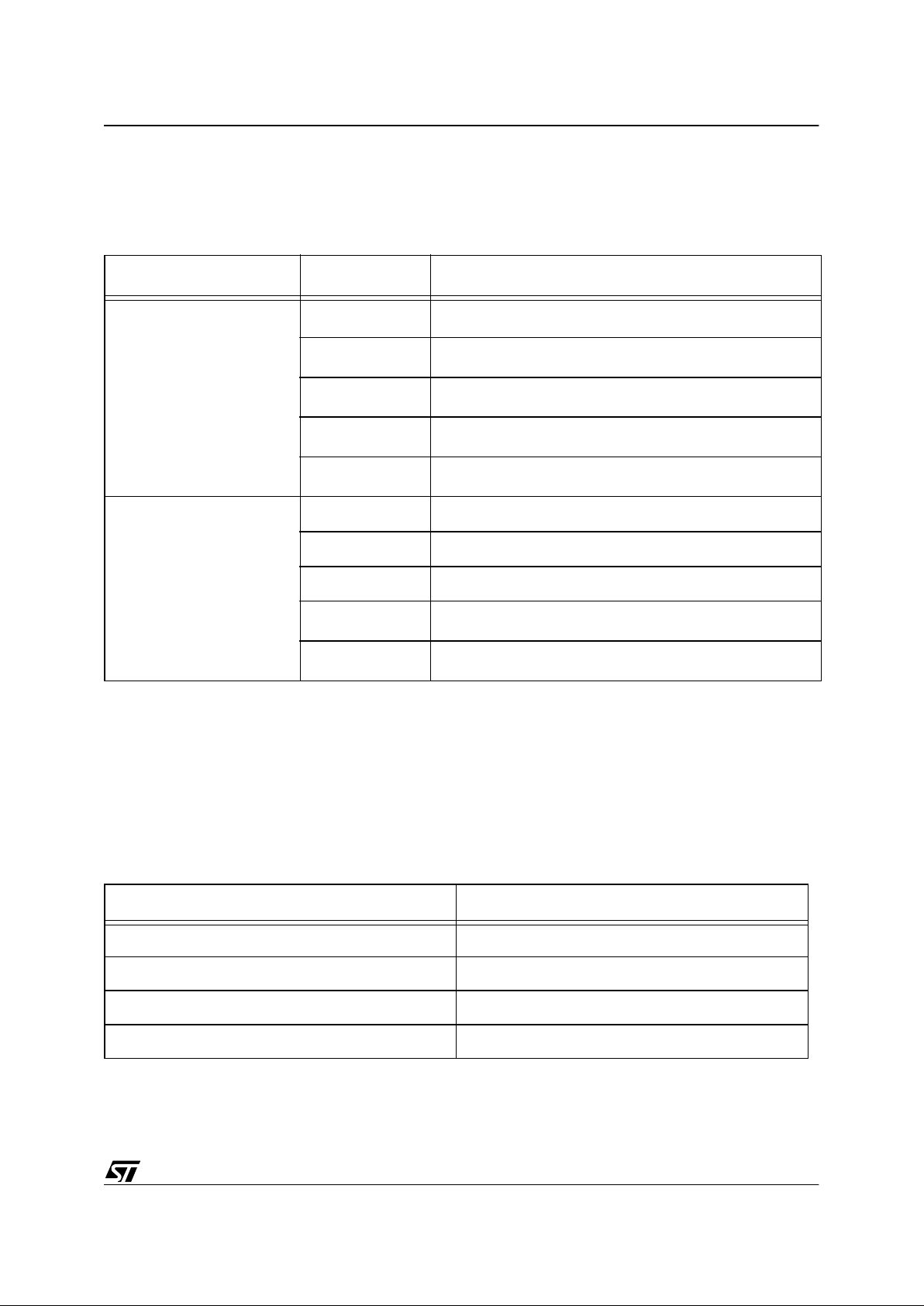
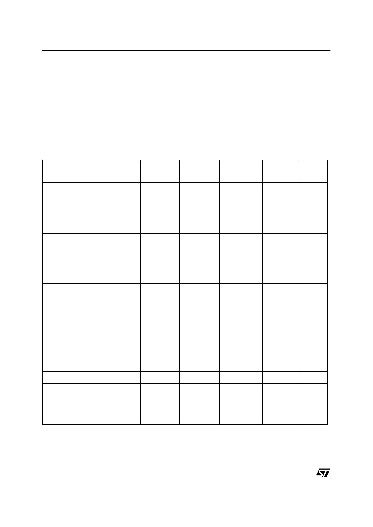
6.1 Interrupt Sources
Source of Interru pt or PEC
Service Request
Request
Flag
Enable
Flag
Interrupt
Vector
Vector
Location
Trap
Number
External Interrupt 0 CC8IR CC8IE CC8INT 60h 18h
External Interrupt 1 CC9IR CC9IE CC9INT 64h 19h
External Interrupt 2 CC10IR CC10IE CC10INT 68h 1Ah
External Interrupt 3 CC11IR CC11IE CC11INT 6Ch 1Bh
GPT1 Timer 2 T2IR T2IE T2INT 88h 22h
GPT1 Timer 3 T3IR T3IE T3INT 8Ch 23h
GPT1 Timer 4 T4IR T4IE T4INT 90h 24h
GPT2 Timer 5 T5IR T5IE T5INT 94h 25h
GPT2 Timer 6 T6IR T6IE T6INT 98h 26h
GPT2 CAPREL Register CRIR CRIE CRINT 9Ch 27h
ASC0 T ransmit S0TIR S0TIE S0TINT A8h 2Ah
ASC0 Transmit Buffer S0TBIR S0 T BIE S0 TB IN T 11Ch 47h
ASC0 Receive S0RIR S0RIE S0RINT ACh 2Bh
ASC0 Error S0EIR S0EIE S0EINT B0h 2Ch
PWM Channel 3 PWMIR PWMIE PWMINT FCh 3Fh
SSP Interrupt XP1IR X P 1IE X P1I NT 104h 41h
PLL Unlock XP3I R XP3IE X P3I NT 10Ch 43h
Table 5 List of possible interrupt sources, flags, vector and trap numbers
1
24/77
ST10R272L - INTERRUPT AND TRAP FUNCTIONS
6.2 Hardware Trap s
Exceptions or error conditions that arise during run-time are called Hardware T raps. Hardware
traps cause immediate non-maskable system reaction similar to a standard interrupt service
(branching to a dedicated vector table location). The occurrence of a hardware trap is
additionally signified by an individual bit in the trap flag register (TFR). Except when another
higher prioritized trap service is in progress, a hardware trap will interrupt any actual progr am
ex ecution. In turn, hardware trap services can not normally be interrupted by standard or PEC
interrupts. The following tab le shows all of the possible ex ceptions or error conditions that can
arise during run-time:
Exception Condition T rap Flag Trap Vector
Vector
Location
Trap
Number
Trap
Priority
Reset Functions:
Hardware Reset RESET 00’0000
h 00h III
Software Reset RESET 00’0000
h 00h III
Watchdog Timer Overflow RESET 00’0000
h 00h III
Class A Hardware Traps:
Non-Maskable Interrupt NMI NMITRAP 00’0008
h 02h II
Stack Overflow STKOF STOTRAP 00’0010
h 04h II
Stack Underflow STKUF STUTRAP 00’0018
h 06h II
Class B Hardware Traps:
Undefined opcode UNDOPC BTRAP 00’0028h 0A
h I
Protected instruction fault PRTFLT BTRAP 00’0028h 0A
h I
Illegal word operand access ILLOPA BTRAP 00’0028h 0A
h I
Illegal instruction access ILLINA BTRAP 00’0028h 0A
h I
Illegal external bus access ILLBUS B TRAP 00’0028h 0A
h I
MAC trap MACTRP BTRAP 00’0028h 0A
h I
Reserved [2C
h – 3Ch][0Bh – 0Fh]
Software Traps
TRAP Instruction Any [00’0000
h
– 00’01FC
h]
steps of 4
h
Any
[00
h – 7Fh]
Current
CPU
Priority
Table 6 Exceptions or error conditions
1
 Loading...