

SGS Thomson Microelectronics ST10F280 Datasheet

1/186
ST10F280
March 2003
■ HIGH PERFORMANCE CPU WITH DSP FUNCTIONS
- 16-BIT CPU WITH 4-STAGE PIPELINE.
- 50ns INSTRUCTION CYCLE TIME AT 40MHz CPU
CLOCK.
- MUL TIPLY/ACCUMULATE U NIT (MAC) 16 X 16-BIT
MULTIPLICATION, 40-BIT ACCUMULATOR
- REPEAT U NI T.
- ENHANCED BOOLEAN BIT MANIPULATION FACILITIES.
- ADDITIO NA L INSTRUC T ION S TO SUPPORT HLL
AND OPERATING SYSTEMS.
- SINGLE-CYCLE CONTEXT SWITCHING SUPPORT.
■ MEMORY ORGANIZATION
- 512K BYT E ON-CHIP FL AS H MEMORY SI NG LE
VOLTAG E WITH ER AS E/ PR O GRAM CONTR O L LER.
- 100K ERASING/PROGRAMMING CYCLES.
- 20 YEAR DAT A RETENTIO N TIME
- UP TO 16M BYTE LINEAR ADDRESS SPACE FOR
CODE AND DATA (5M BYTE WITH CAN).
- 2K BYTE ON -CH IP INT ER NAL RA M (IRA M).
- 16K BYTE EXT EN SI O N RAM (XRA M ).
■ FAST AND FLEXIBLE BUS
- PROGRAMMABLE EXTERNAL BUS CHARACTERISTICS FOR DIFFERENT ADDRESS RANGES.
- 8-BIT OR 16-BIT EXTERNAL DATA BUS.
- MULTIPLEXED OR DEMULTIPLEXED EXTERNAL
ADDRESS/DATA BUSES.
- FIVE PROGRAMMABLE CHIP-SELECT SIGNALS.
- HOLD-ACKNOWLEDGE BUS ARBITRATION SUPPORT.
■ INTERRUPT
- 8-CHANNEL PERIPHERAL EVENT CONTROLLER
FOR SINGLE CYCLE, INTERRUPT DRIVEN DATA
TRANSFER.
- 16-PRIORITY-LEVEL INTERRUPT SYSTEM WITH 56
SOURCES, SAMPLE-RATE DOWN TO 25ns.
■ TWO MULTI-FUNCTIONAL GENERAL PURPOSE
TIMER UNITS WITH 5 TIMERS.
■ TWO 16-CHANNEL CAPTURE/COMPARE UNITS
■ A/D CONVERTER
- 2X16-CHANNEL 10-BIT.
- 4.85µS CONVERSION TIME
- ONE TIMER FOR ADC CHANNEL INJEC TI ON
■ 8-CHANNEL PWM UNIT
■ SERIAL CHANNELS
- SYNCHRONOUS/ASYNC SERIAL CHANNEL
- HIGH-SPEED SYNCHRONOUS CHANNEL.
■ FAIL-SAFE PROTECTIO N
- PROGRAMMABLE WATCHDOG TIMER.
- OSCILLATOR WATCHDOG.
■ TWO CAN 2.0b INTERFACES OPERATING ON ONE
OR TWO CAN BUSSES (30 OR 2X15 MESSAGE
OBJECTS)
■ ON-CHIP BOOTSTRAP LOADER
■ CLOCK GENERA TION
- ON-CHIP PL L .
- DIRECT OR PRESCALED CLOCK INPUT.
■ UP TO 143 GENERAL PUR PO SE I/O LINES
- INDIVIDUALLY PROGRAMMABLE AS INPUT, OUTPUT OR SPECIAL FUNCTION.
- PROGRAMMABLE THRESHOLD (HYSTERESIS).
■ IDLE AND POWE R DOWN M OD ES
■ MAXIMUM CP U FR EQUE NC Y 40 MH z
■ PACKAGE PBGA 208 BALLS (23mm x 23mm x
1.96 mm - PITCH 1.27mm).
■ SINGLE VOLTAGE SUPPLY: 5V ±10% (EMBEDDED
REGULATOR FOR 3.3 V CORE SUPPLY).
■ TEMPERATURE RANGE: -40 +125
°
C
PBGA208 (23 x 23 x 1.96 - Pitch 1.27 mm)
(Plastic Bold Grid Array)
ORDER CO DE: ST10F280-JT3
P4.7 CA N2_TxD
P4.6 CA N1_TxD
P4.5 CA N1_R x D
P4.4 CA N2_R x D
Port 0Port 1Port 4
Port 6
Port 5
Port 3
Port 2
GPT1
GPT2
ASC usart
BRG
CPU-Core and MAC Unit
Internal
RAM
Watchdog
Interrupt Controller
8
32 16
PEC
16
16
CAN1
Port 7 Port 8
External Bus
10-Bit ADC
BRG
SSC
PWM
CAPCOM2
CAPCOM1
16
Oscillator
Controller
16
16
512K Byte
and PLL
Flash Memory
XTAL1 XTAL2
2K Byte
15
8
8
8
16
3.3V Voltage
Regulator
16K Byte
XRAM
CAN2
XPORT916XPWM4XTIMER
P7.7 T rigge r fo r A D C
16
XPORT10
16
16
cha nnel injection
XADCINJ
External connexion
16-BIT MCU WITH MAC UNIT, 512K BYTE FLASH MEMORY AND 18K BY TE RAM
PRODUCT PREVIEW
This is advance information on a new product now in development or undergoing evaluation. Details are subject to change without notice.

ST10F280
2/186
TABLE OF CONTENTS
1 - INTRODUCTION ........... ................. ................ ........................ ................. ................... 6
2 - BALL DATA .. ................ ................. ....................... ................. ........................ ............ 7
3 - FUNCTIONAL DESCRIPTION ................ ................. ................ .......... ................ ........ 17
4 - MEMORY ORGANIZATION ....................................................................................... 18
5 - INTERNAL FLASH MEMORY ................ ................. ......... ................. ................ ........ 21
5.1 - OVERVIEW ................................................................................................................ 21
5.2 - OPERATIONAL OVERVIEW ...................................................................................... 21
5.3 - ARCHITECTURAL DESCRIPTION ............................................................................ 23
5.3.1 - Read Mode ................................................................................................................. 23
5.3.2 - Command Mode ......................................................................................................... 23
5.3.3 - Flash Status Register ................................................................................................. 23
5.3.4 - Flash Protection Register ........................................................................................... 25
5.3.5 - Instructions Description .............................................................................................. 25
5.3.6 - Reset Processing and Initial State .............................................................................. 29
5.4 - FLASH MEMORY CONFIGURATION ........................................................................ 29
5.5 - APPLICATION EXAMPLES ....................................................................................... 29
5.5.1 - Handling of Flash Addresses . ..................................................................................... 29
5.5.2 - Basic Flash Access Control ........................................................................................ 30
5.5.3 - Programming Examples ............................................................................................. 31
5.6 - BOOTSTRAP LOADER ............................................................................................ 34
5.6.1 - Entering the Bootstrap Loader .................................................................................... 34
5.6.2 - Memory Configuration After Reset ............................................................................. 35
5.6.3 - Loading the Startup Code ........................................................................................... 36
5.6.4 - Exiting Bootstrap Loader Mode .................................................................................. 36
5.6.5 - Choosing the Baud Rate for the BSL ......................................................................... 37
6 - CENTRAL PROCESSING UNIT (CPU) ..................................................................... 38
6.1 - MULTIPLIER-ACCUMULATOR UNIT (MAC) ............................................................. 39
6.1.1 - Features ..................................................................................................................... 40
6.1.1.1 - Enhanced Addressing Capab ilit ies.............................................................................. 40
6.1.1.2 - Multiply-Accumulate Unit............................................................................................. 40
6.1.1.3 - Program Control. ........................ ................. ....................... ................. ........................ 40
6.2 - INSTRUCTION SET SUMMARY ................................................................................ 41
6.3 - MAC COPROCESSOR SPECIFIC INSTRUCTIONS ................................................. 42
7 - EXTERNAL BUS CONTROLLER ............................ ......... ................. ................ ........ 46
7.1 - PROGRAMMABLE CHIP SELECT TIMING CONTROL ............................................ 46
7.2 - READY PROGRAMMABLE POLARITY ..................................................................... 47
8 - INTERRUPT SYSTEM ..... ................ ........................ ................ ........................ .......... 49
8.1 - EXTERNAL INTERRUPTS ......................................................................................... 49

ST10F280
3/186
8.2 - INTERRUPT REGISTERS AND VECTORS LOCATION LIST .................................. 50
8.3 - INTERRUPT CONTROL REGISTERS ....................................................................... 52
8.4 - EXCEPTION AND ERROR TRAPS LIST ................................................................... 53
9 - CAPTURE/COMPARE (CAPCOM) UNITS ................................................................ 54
10 - GENERAL PURPOSE TIMER UNIT .......................................................................... 57
10.1 - GPT1 .......................................................................................................................... 57
10.2 - GPT2 .......................................................................................................................... 58
11 - PWM MODULE .................. ........................ ................ ........................ ................ ........ 60
11.1 - STANDARD PWM MODULE ...................................................................................... 60
11.2 - NEW PWM MODULE : XPWM ................................................................................... 61
11.2.1 - Operating Modes ........................................................................................................62
11.2.1.1 - Mode 0: Standard PWM Generation (Edge Aligned PW M)......................................... 62
11.2.1.2 - Mode 1: Symmetrical PWM Generation (Ce nter Aligned PW M) ................................. 63
11.2.1.3 - Burst Mode ................................................................................................................ 64
11.2.1.4 - Single Shot Mode .... ........................ ................. ....................... ................. ................. 65
11.2.2 - XPWM Module Registers ........................................................................................... 66
11.2.3 - Interrupt Request Generation ..................................................................................... 68
11.2.4 - XPWM Output Signals ................................................................................................ 68
11.2.5 - XPOLAR Register (polarity of the XPWM channel) .................................................... 69
12 - PARALLEL PORTS ........... ................ ........................ ................. ....................... ........ 70
12.1 - INTRODUCTION ........................................................................................................ 72
12.1.1 - Open Drain Mode ....................................................................................................... 72
12.1.2 - Input Threshold Control ............................................................................................ 73
12.1.3 - Output Driver Control ................................................................................................73
12.1.4 - Alternate Port Functions ............................................................................................. 75
12.2 - PORT0 ........................................................................................................................ 76
12.2.1 - Alternate Functions of PORT0 .................................................................................... 77
12.3 - PORT1 ........................................................................................................................ 79
12.3.1 - Alternate Functions of PORT1 .................................................................................... 79
12.4 - PORT 2 ....................................................................................................................... 80
12.4.1 - Alternate Functions of Port 2 ..................................................................................... 81
12.5 - PORT 3 ....................................................................................................................... 84
12.5.1 - Alternate Functions of Port 3 ...................................................................................... 85
12.6 - PORT 4 ....................................................................................................................... 87
12.6.1 - Alternate Functions of Port 4 ...................................................................................... 88
12.7 - PORT 5 ....................................................................................................................... 92
12.7.1 - Port 5 Schmitt Trigger Analog Inputs .......................................................................... 93
12.8 - PORT 6 ....................................................................................................................... 93
12.8.1 - Alternate Functions of Port 6 ...................................................................................... 94
12.9 - PORT 7 ....................................................................................................................... 95
12.9.1 - Alternate Functions of Port 7 ...................................................................................... 96

ST10F280
4/186
12.10 - PORT 8 .......... ................ ................. ....................... ................. ........................ ............ 99
12.10.1 - Alternate Functions of Port 8 ...................................................................................... 99
12.11 - XPORT 9 .................................................................................................................... 101
12.12 - XPORT 10 .................................................................................................................. 103
12.12.1 - Alternate Functions of XPort 10 .................................................................................. 103
12.12.2 - New Disturb Protection on Analog Inputs ................................. ....... ..... ....... ....... ..... ... 104
13 - A/D CONVERTER ................... ....................... ................. ........................ ................ ... 105
13.1 - A/D CONVERTER MODULE ...................................................................................... 105
13.2 - MULTIPLEXAGE OF TWO BLOCKS OF 16 ANALOG INPUTS ................................ 106
13.3 - XTIMER PERIPHERAL (TRIGGER FOR ADC CHANNEL INJECTION) ................... 107
13.3.1 - Main Features ............................................................................................................. 107
13.3.2 - Register Description ...................................................................................................108
13.3.2.1 - TCR : Timer Control Register...................................................................................... 108
13.3.2.2 - XTSVR :Timer Start Value Register............................................................................ 109
13.3.2.3 - XTEVR : Timer End Value Regist e r.............. ........................ ................ ...................... 109
13.3.2.4 - XTCVR : Timer Current Value Register....................................................................... 109
13.3.2.5 - Registers Mapping....................................................................................................... 109
13.3.3 - Block Diagram ........................................................................................................... 110
13.3.3.1 - C l o cks........ ................ ........................ ................. ....................... ................. ....... .......... 110
13.3.3.2 - R e g i ste r s........ ....................... ................. ........................ ................ ............................. 110
13.3.3.3 - Timer output (XADCINJ).............................................................................................. 111
14 - SERIAL CHANNELS .............. ................ ........................ ........................ ................ ... 112
14.1 - ASYNCHRONOUS / SYNCHRONOUS SERIAL INTERFACE (ASCO) .................... 112
14.1.1 - ASCO in Asynchronous Mode .................................................................................... 112
14.1.2 - ASCO in Synchronous Mode ...................................................................................... 114
14.2 - HIGH SPEED SYNCHRONOUS SERIAL CHANNEL (SSC) .......... .......... ................. 116
15 - CAN MODULES ... ................ ........................ ................. ................ ........................ ..... 118
15.1 - MEMORY MAPPING .................................................................................................. 1 18
15.1.1 - CAN1 .......................................................................................................................... 118
15.1.2 - CAN2 .......................................................................................................................... 118
15.2 - CAN BUS CONFIGURATIONS .................................................................................. 118
15.3 - REGISTER AND MESSAGE OBJECT ORGANIZ AT IO N ........................... ............... 119
15.4 - CAN INTERRUPT HANDLING ................................................................................. 121
15.5 - THE MESSAGE OBJECT .......................................................................................... 124
15.6 - ARBITRATION REGISTERS ...................................................................................... 126
16 - WATCHDOG TIMER ............................. ................ ................. ........................ ............ 127
17 - SYSTEM RESET ........................................................................................................ 129
17.1 - ASYNCHRONOUS RESET (LONG HARDWARE RESET) ....................................... 129
17.2 - SYNCHRONOUS RESET (WARM RESET) .............................................................. 130

ST10F280
5/186
17.3 - SOFTWARE RESET .................................................................................................. 131
17.4 - WATCHDOG TIMER RESET ..................................................................................... 131
17.5 - RSTOUT PIN AND BIDIRECTIONAL RESET ............................................................ 131
17.6 - RESET CIRCUITRY ................................................................................................... 132
18 - POWER REDUCTION MODES ................................................................................. 135
18.1 - IDLE MODE ................................................................................................................135
18.2 - POWER DOWN MODE .............................................................................................. 135
18.2.1 - Protected Power Down Mode ..................................................................................... 136
18.2.2 - In terruptable Power Down Mode ................................................................................ 136
19 - SPECIAL FUNCTION REGISTER OVERVIEW ......................................................... 139
19.1 - IDENTIFICATION REGISTERS ................................................................................. 148
19.2 - SYSTEM CONFIGURATION REGISTERS ................................................................ 149
20 - ELECTRICAL CHARACTERISTICS ............. ................. ................ .......... ................. 155
20.1 - ABSOLUTE MAXIMUM RATINGS ............................................................................. 155
20.2 - PARAMETER INTERPRETATION ............................................................................. 155
20.3 - DC CHARACTERISTICS ........................................................................................... 155
20.3.1 - A/D Converter Characteristics .................................................................................... 158
20.3.2 - Conversion Timing Control ....................................................................................... 159
20.4 - AC CHARACTERISTICS ............................................................................................ 160
20.4.1 - Test Waveforms .......................................................................................................160
20.4.2 - Definition of Internal Timing ........................................................................................ 160
20.4.3 - Clock Generation Modes ............................................................................................ 1 61
20.4.4 - Prescaler Operation ....................................................................................................162
20.4.5 - Direct Drive ................................................................................................................. 162
20.4.6 - Osc illator Watchdog (OW D ) ....................................................................................... 162
20.4.7 - Phase Locked Loop .................................................................................................... 162
20.4.8 - External Clock Drive XTAL1 ....................................................................................... 163
20.4.9 - Memory Cycle Variables ............................................................................................. 164
20.4.10 - Multiplexed Bus .......................................................................................................... 165
20.4.11 - Demultiplexed Bus ...................................................................................................... 171
20.4.12 - CLKOUT and READY ................................................................................................. 177
20.4.13 - External Bus Arbitration ..............................................................................................179
20.4.14 - High-Speed Synchronous Serial Interface (SSC) Timing ........................................... 181
20.4.14.1 Master Mode................................................................................................................ 181
20.4.14.2 Slave mode.................................................................................................................. 182
21 - PACKAGE MECHANICAL DATA ...................... .......... ................ .......... ................. 183
22 - ORDERING INFORMATION ...................................................................................... 1 84
ST10F280
6/186
1 - INTRODUCTION
The ST10F280 is a new derivative of the ST
Microelectronics ST10 family of 16-bit single-chi p
CMOS microcontrollers. It combines high CPU
performance (up to 20 million instructions per
second) with high peripheral functionality and
enhanced I/O-capabilities. It also provides on-chip
high-speed single voltage FLASH memory,
on-chip high-speed RAM, and clock generation
via PLL.
ST10F280 is processed in 0.35µm CMOS
technology. The MCU core and the logic is
supplied with a 5V to 3.3V on chip voltage
regulator. The part is supplied with a single 5V
supply and I/Os work at 5V .
The device is upward compatible with the
ST10F269 device, with the following set of
differences:
– Two supply pins (DC1,DC2) on the PBGA-208
package are used for decoupling the internally
generated 3.3V core logic supply. Do not connect these two pins to 5. 0V external suppl y. Instead, these pins should be connected to a
decoupling capacitor (ceramic type, value
≥ 330nF).
– The A/D Converter characteristics stay identical
but 16 new input channel are added. A bit in a
new register (XADCMUX) control the multiplexage between the first b lock of 16 channel (on
Port5) and the second block (on XPort10). The
conversion result registers stay identical and the
software management can determine the block
in use. A new dedicated timer controls now the
ADC channel injection mode on the inp ut CC 31
(P7.7). The output of this timer is visible on a
dedicated pin (XADCINJ) to emulate this new
functionnality.
– A second XPWM peripheral (4 new channels) is
added. Four dedicated pins are reserved for the
outputs (XPWM[0:3])
– A new general purpose I/O port named XPORT9
(16 bits) is added. Due to the bit addressing
management, it will be different from other
standard general purpose I/O ports.
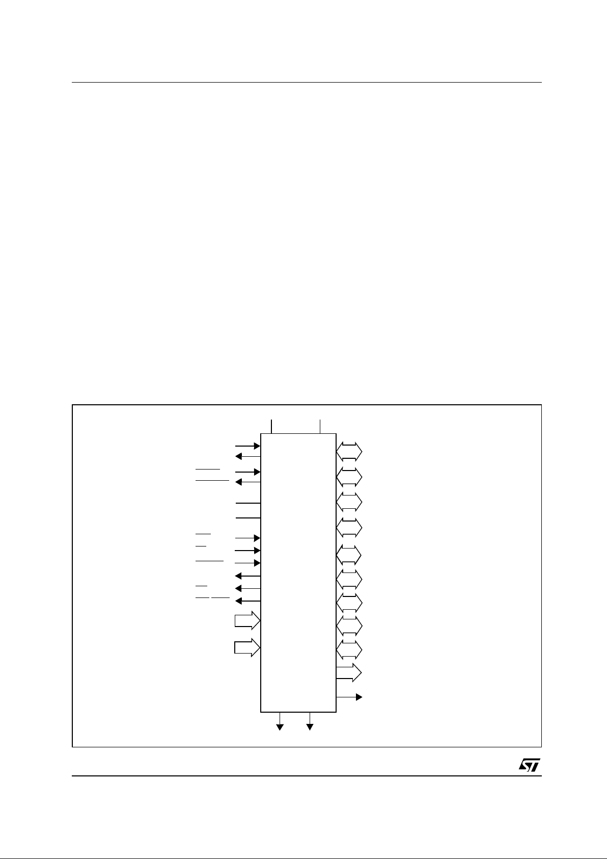
Figure 1 : Logic Symbol
XTAL1
RSTIN
XTAL2
RSTOUT
NMI
EA
READY
ALE
RD
WR/WRL
Port 5
16-bit
Port 6
8-bit
Port 4
8-bit
Port 3
15-bit
Port 2
16-bit
Port 1
16-bit
Port 0
16-bit
V
DD
V
SS
Port 7
8-bit
Port 8
8-bit
V
AREF
V
AGND
XPort 9
16-bit
XPWM
4-bit
XADCINJ
XPort10
16-bit
DC1
DC2
Decoupling capacitor for internal regulator
ST10F280
ST10F280
7/186
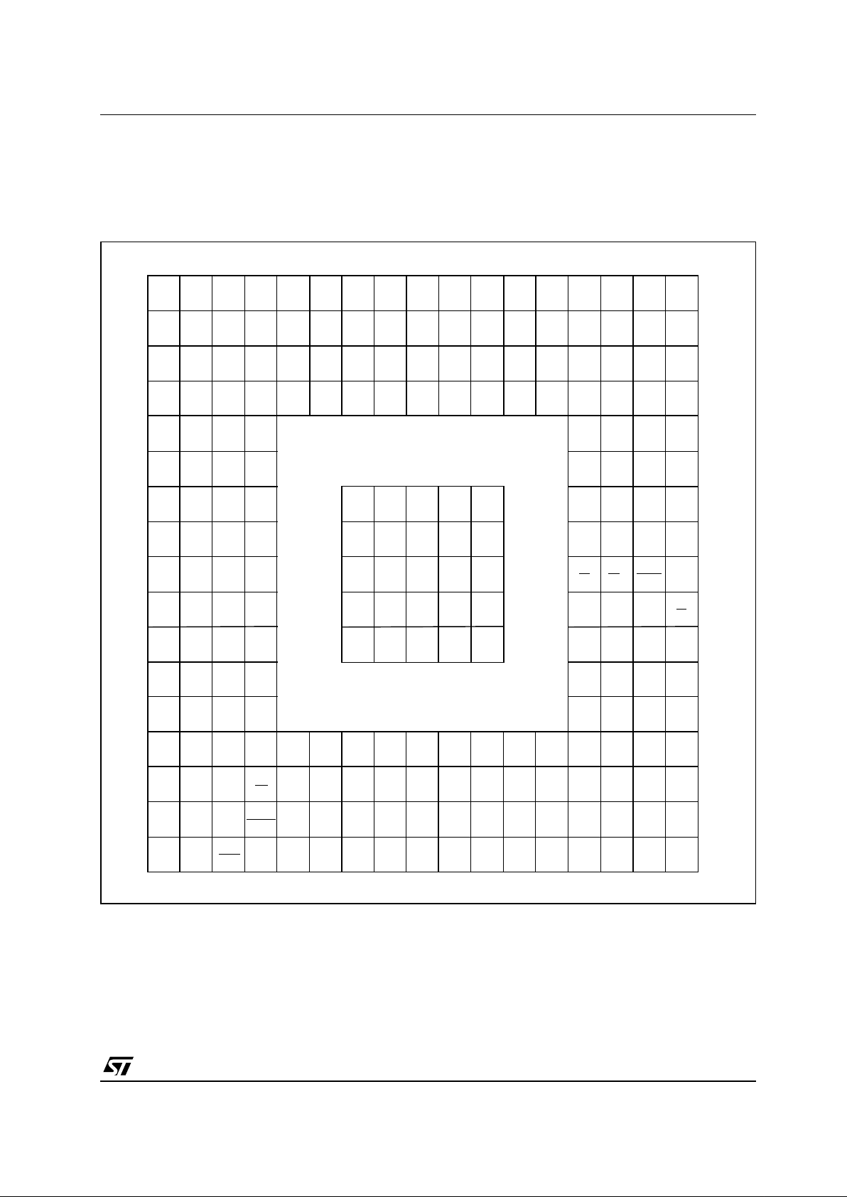
2 - BALL DATA
The ST10F280 package is a PB GA of 23 x 23 x 1.96 mm . The pitch of the balls is 1. 27 mm. The s ignal
assignment of the 208 balls is described in Figure 2 for the configuration and in Tabl e 1 for the ball signal
assignment. This package has 25 additional therm al balls.
Figure 2 : Ball Configuration (bottom view)
K7
V
SS
K8
V
SS
K9
V
SS
J7
V
SS
J8
V
SS
J9
V
SS
H7
V
SS
H8
V
SS
H9
V
SS
G7
V
SS
G8
V
SS
G9
V
SS
K10
V
SS
K11
V
SS
J10
V
SS
J11
V
SS
H10
V
SS
H11
V
SS
G10
V
SS
G11
V
SS
VSSVSSVSSVSSV
SS
U1 U2
V
AREF
U3
V
AGND
U4 U5 U6 U7 U8 U9 U1 0
V
SS
U11
DC2
U12 U13 U14 U15 U16
T1 T2 T3 T4 T5 T6 T7 T8 T9 T10 T11 T12 T13 T14 T15 T16
R1 R2 R3
R4
R14 R15 R16
M1 M2 M3
M15 M16 M17
L1
V
SS
L2 L3
L15 L16 L17
V
DD
K1
V
DD
K2 K3
K15 K16 K17
V
SS
J1 J2 J3
J15 J16 J17
H1 H2 H3
H15 H16 H17
G1 G2 G3
G15 G16 G17
F1 F2 F3
F15 F16 F17
E1 E2 E3
E15 E16 E17
V
SS
D1 D2 D3
D15 D16 D17
C1 C2 C3 C4 C5 C6 C7 C8 C9 C10 C1 1 C12 C13 C14 C15 C16
B1 B2 B3 B4 B5 B6 B7 B8 B9 B10 B11 B12 B13 B14 B15 B16
A1 A2 A3 A4
RSTIN
A5
XTAL1A6XTAL2
A7 A8 A9 A10 A11 A12 A13 A14 A15 A16
A
B
C
D
E
F
G
H
J
K
L
M
N
P
R
T
A
B
C
D
E
F
G
H
J
K
L
M
N
P
R
T
1716151413121110987654321
1716151413121110987654321
U17
T17
R17
C17
B17
A17
U
U
V
SS
DC1 V
DD
M4
L4
K4
J4
H4
G4
E4
D4
M14
L14
K14
J14
H14
G14
E14
D14
P15 P16 P17
P14
D5 D6 D7 D8 D9 D10 D11 D12 D13
P5 P6 P7 P8 P9 P10 P11 P12 P13
N1 N2 N3
N4
F4
F14
L7 L8 L9 L10 L11
V
DD
V
DD
V
SS
V
DD
V
SS
V
DD
V
SS
V
DD
V
SS
VSSV
DD
VSSV
DD
P3.15
V
DD
V
SS
RPD
XP10.3 XP10.2 XP10.1 XP10.0
XP10.4XP10.5XP10.6XP10.7
XP10.11 XP10.8 P5.6 P5.10 P5.14XP10.9XP10.10
XP10.13 XP10.12 P5.1 P5.3 P5.7 P5.11 P5.15
XP10.14 P5.0 P5.2 P5.4 P5.8 P5.12
XP10.15 P5.5 P5.9 P5.13
xpwm.0
xpwm.1
xpwm.2
xpwm.3
P6.0
P6.1
P6.2
P6.3
P6.4
P6.5
P6.6
P6.7
P8.0
P8.1P8.2
P8.3P8.4
P8.5P8.6P8.7
P7.0P7.1P7.2P7.3
P7.4 P7.5 P7.6
P7.7 XADCINJ
P2.0
P2.1
P2.2
P2.3 P2.4
P2.5
P2.6
P2.7
P2.8
P2.9
P2.10
P2.11
P2.12
P2.13
P2.14
P2.15
P3.0
P3.1
P3.2
P3.3
P3.4
P3.5
P3.6
P3.7
P3.8 P3.9
P3.10
P3.11 P3.12
P3.13
P4.0
P4.1
P4.2
P4.3
P4.4 P4.5
P4.6 P4.7
RD WR READY ALE
EAP0.0P0.1P0.2
P0.3P0.4P0.5
P0.6
P0.7
P0.8
P0.9
P0.10
P0.11
P0.12
P0.13
P0.14
P0.15
XP9.0
XP9.1
XP9.2
XP9.3
XP9.4
XP9.5
XP9.6
XP9.7
XP9.8
XP9.9
XP9.10
XP9.11
XP9.12
XP9.13
XP9.14
XP9.15
P1.0
P1.1
P1.2
P1.3
P1.4
P1.5
P1.6
P1.7P1.8
P1.9
P1.10
P1.11
P1.12
P1.13
P1.14 P1.15
V
SS
RSTOUT
NMI
V
SS
V
SS
V
SS
VSSV
SS
VSSV
SS
V
SS
V
SS
V
SS
V
SS
VSSV
SS
V
SS
V
SS
V
SS
VSSV
SS
V
SS
V
SSVSS
R5 R6 R7 R8 R9 R10 R11 R12 R13
N15 N16 N17
N14
P1 P2 P3 P4

ST10F280
8/186
Table 1 : Ball Descri pti o n
Symbol
Ball
Number
Type Function
P6.0 – P6.7 I/O Port 6 is an 8 -bit bidirectional I/O port. It is bit-wise programmable for input or
output via direction bits. For a pin configured as input, the output driver is put into
high-impedance state. Port 6 outputs can be configured as push/pull or open
drain drivers.
The following Port 6 pins also serve for alternate functions:
E4 O P6.0 CS0
Chip Select 0 Output
D3 O P6.1 CS1 Chip Select 1 Output
B1 O P6.2 CS2
Chip Select 2 Output
C1 O P6.3 CS3 Chip Select 3 Output
D2 O P6.4 CS4
Chip Select 4 Output
E3 I P6.5 HOLD External Master Hold Request Input
F4 O P6.6 HLDA
Hold Acknowledge Output
D1 O P6.7 BREQ Bus Request Output
P8.0 – P8.7 I/O Port 8 is an 8 -bit bidirectional I/O port. It is bit-wise programmable for input or
output via direction bits. For a pin configured as input, the output driver is put into
high-impedance state. Port 8 outputs can be configured as push/pull or open
drain drivers. The input threshold of Port 8 is selectable (TTL or special).
The following Port 8 pins also serve for alternate functions:
E2 I/O P8.0 CC16IO CAPCOM2: CC16 Capture Input / Compare Output
F3 I/O P8.1 CC17IO CAPCOM2: CC17 Capture Input / Compare Output
F2 I/O P8.2 CC18IO CAPCOM2: CC18 Capture Input / Compare Output
G3 I/O P8.3 CC19IO CAPCOM2: CC19 Capture Input / Compare Output
G2 I/O P8.4 CC20IO CAPCOM2: CC20 Capture Input / Compare Output
H4 I/O P8.5 CC21IO CAPCOM2: CC21 Capture Input / Compare Output
H3 I/O P8.6 CC22IO CAPCOM2: CC22 Capture Input / Compare Output
H2 I/O P8.7 CC23IO CAPCOM2: CC23 Capture Input / Compare Output
P7.0 – P7.7 I/O Port 7 is an 8 -bit bidirectional I/O port. It is bit-wise programmable for input or
output via direction bits. For a pin configured as input, the output driver is put into
high-impedance state. Port 7 outputs can be configured as push/pull or open
drain drivers. The input threshold of Port 7 is selectable (TTL or special).
The following Port 7 pins also serve for alternate functions:
J4 O P7.0 POUT0 PWM Channel 0 Output
J3 O P7.1 POUT1 PWM Channel 1 Output
J2 O P7.2 POUT2 PWM Channel 2 Output
J1 O P7.3 POUT3 PWM Channel 3 Output
K2 I/O P7.4 CC28IO CAPCOM2: CC28 Capture Input / Compare Output
K3 I/O P7.5 CC29IO CAPCOM2: CC29 Capture Input / Compare Output
K4 I/O P7.6 CC30IO CAPCOM2: CC30 Capture Input / Compare Output
L2 I/O P7.7 CC31IO CAPCOM2: CC31 Capture Input / Compare Output

ST10F280
9/186
XP10.0 – XP10.15 I XPort 10 is a 16-bit input-only port with Schmitt-Trigger characteristics.
The pins of X Port10 also serve as the analo g input c hannels (up to 16) for the
A/D converter, where XP10.X equals ANx (Analog input channel x).
M4
M3
M2
M1
N4
N3
N2
N1
P4
P3
P2
P1
R2
R1
T1
U1
I
I
I
I
I
I
I
I
I
I
I
I
I
I
I
I
XP10.0
XP10.1
XP10.2
XP10.3
XP10.4
XP10.5
XP10.6
XP10.7
XP10.8
XP10.9
XP10.10
XP10.11
XP10.12
XP10.13
XP10.14
XP10.15
P5.0 – P5.15 I Port 5 is a 16-bit input-only port with Schmitt-Trigger characteristics.
The pins of Port 5 also ser ve as the analog inp ut chann els (up to 16) for the A/D
converter, where P5.x equals ANx (Analog input channel x),
or they serve as timer inputs:
T2 I P5.0
R3 I P5.1
T3 I P5.2
R4 I P5.3
T4 I P5.4
U4 I P5.5
P5 I P5.6
R5 I P5.7
T5 I P5.8
U5 I P5.9
P6 I P5.10 T6EUD GPT2 Timer T6 External Up / Down Control Input
R6 I P5.11 T5EUD GPT2 Timer T5 External Up / Down Control Input
T6 I P5.12 T6IN GPT2 Timer T6 Count Input
U6 I P5.13 T5IN GPT2 Timer T5 Count Input
P7 I P5.14 T4EUD GPT1 Timer T4 External Up / Down Control Input
R7 I P5.15 T2EUD GPT1 Timer T2 External Up / Down Control Input
Table 1 : Ball Description (continued)
Symbol
Ball
Number
Type Function

ST10F280
10/186
P2.0 – P2.15 I/O Port 2 is a 16 -bit bidirectional I/O port. It is bit-wise programmable for input or
output via direction bits. For a pin configured as input, the output driver is put into
high-impedance state. Port 2 outputs can be configured as push/pull or open
drain drivers. The input threshold of Port 2 is selectable (TTL or special).
The following Port 2 pins also serve for alternate functions:
T7 I/O P2.0 CC0IO CAPCOM: CC0 Capture Input / Compare Output
P8 I/O P2.1 CC1IO CAPCOM: CC1 Capture Input / Compare Output
R8 I/O P2.2 CC2IO CAPCOM: CC2 Capture Input / Compare Output
T8 I/O P2.3 CC3IO CAPCOM: CC3 Capture Input / Compare Output
T9 I/O P2.4 CC4IO CAPCOM: CC4 Capture Input / Compare Output
P9 I/O P2.5 CC5IO CAPCOM: CC5 Capture Input / Compare Output
R9 I/O P2.6 CC6IO CAPCOM: CC6 Capture Input / Compare Output
U9 I/O P2.7 CC7IO CAPCOM: CC7 Capture Input / Compare Output
T10 I/OIP2.8 CC8IO CAPCOM: CC8 Capture Input / Compare Output,
EX0IN Fast External Interrupt 0 Input
R10 I/OIP2.9 CC9IO CAPCOM: CC9 Capture Input / Compare Output,
EX1IN Fast External Interrupt 1 Input
P10 I/OIP2.10 CC10IO CAPCOM: CC10 Capture Input / Compare Output,
EX2IN Fast External Interrupt 2 Input
T11 I/OIP2.11 CC11IO CAPCOM: CC11 Capture Input / Compare Output,
EX3IN Fast External Interrupt 3 Input
R11 I/OIP2.12 CC12IO CAPCOM: CC12 Capture Input / Compare Output,
EX4IN Fast External Interrupt 4 Input
U12 I/OIP2.13 CC13IO CAPCOM: CC13 Capture Input / Compare Output,
EX5IN Fast External Interrupt 5 Input
P11 I/OIP2.14 CC14IO CAPCOM: CC14 Capture Input / Compare Output,
EX6IN Fast External Interrupt 6 Input
T12 I/O
I
I
P2.15 CC15IO CAPCOM: CC15 Capture Input / Compare Output,
EX7IN Fast External Interrupt 7 Input
T7IN CAPCOM2 Timer T7 Count Input
Table 1 : Ball Description (continued)
Symbol
Ball
Number
Type Function

ST10F280
11/186
P3.0 - P3.13,
P3.15
I/O Port 3 is a 15-bit (P 3.14 is missi ng) bidirecti onal I/O por t. It i s bit-wise pro gram-
mable for input or output via direction bits. For a pin configured as input, the out-
put driver is put in to high-imp edance st ate. Port 3 outputs ca n be config ured as
push/pull or open drain dri vers. The input threshold of Port 3 is select able (TTL
or special).
The following Port 3 pins also serve for alternate functions:
R12 I P3.0 T0IN CAPCOM Timer T0 Count Input
T13 O P3.1 T6OUT GPT2 Timer T6 Toggle Latch Output
P12 I P3.2 CAPIN GPT2 Register CAPREL Capture Input
R13 O P3.3 T3OUT GPT1 Timer T3 Toggle Latch Output
T14 I P3.4 T3EUD GPT1 Timer T3 External Up / Down Control Input
P13 I P3.5 T4IN GPT1 Timer T4 Input for Count / Gate /
Reload / Capture
R14 I P3.6 T3IN GPT1 Timer T3 Count / Gate Input
P14 I P3.7 T2IN GPT1 Timer T2 Input for Count / Gate /
Reload / Capture
R15 I/O P3.8 MRST SSC Master-Receive / Slave-Transmit I/O
R16 I/O P3.9 MTSR SSC Master-Transmit / Slave-Receive O/I
N14 I/O P3.10 TxD0 ASC0 Clock / Data Output (Asynchronous / Synchronous)
P15 O P3.11 RxD0 ASC0 Data Input (Asynchronous) or I/O (Synchronous)
P16 O P3.12 BHE
External Memory High Byte Enable Signal,
WRH
External Memory High Byte Write Strobe
M14 I/O P3.13 SCLK SSC Master Clock Output / Slave Clock Input
T17 O P3.15 CLKOUT System Clock Output (=CPU Clock)
P4.0 – P4.7 I/O Port 4 is an 8 -bit bidirectional I/O port. It is bit-wise programmable for input or
output via direction bits. For a pin configured as input, the output driver is put into
high-impedance state. The input threshold is selectable (TTL or special).
P4.6 & P4.7 outputs can be configured as push-pull or open-drain drivers.
In case of an exter nal bus configuration, Por t 4 can be us ed to output the se g-
ment address lines:
N16 O P4.0 A16 Least Significant Segment Address Line
M15 O P4.1 A17 Segment Address Line
L14 O P4.2 A18 Segment Address Line
M16 O P4.3 A19 Segment Address Line
L15 OIP4.4 A20 Segment Address Line
CAN2_RxD CAN2 Receive Data Input
L16 OIP4.5 A21 Segment Address Line
CAN1_RxD CAN1 Receive Data Input
K14 OOP4.6 A22 Segment Address Line, CAN_TxD
CAN1_TxD CAN1 Transmit Data Output
K15 OOP4.7 A23 Most Significant Segment Address Line
CAN2_TxD CAN2 Transmit Data Output
Table 1 : Ball Description (continued)
Symbol
Ball
Number
Type Function

ST10F280
12/186
RD
J14 O External Memory Read Strobe. RD is activated for every external instruction or
data read access.
WR
/WRL J15 O External Memory Write Strobe. In WR-mode this pin is activated for every
external data write access. In WRL
-mode this pin is activated for low byte data
write accesses on a 16-bit bus, and for every data write access on an 8-bit bus.
See WRCFG in register SYSCON for mode selection.
READY/
READY
J16 I Ready Input. The active level is programmable. When the Ready function is
enabled, the selected inactive level at this pin during an external memory access
will force the insertion of memory cycle time waitstates until the pin returns to the
selected active level.
ALE J17 O Address Latch Enable Output. Can be used for latching the address into external
memory or an address latch in the multiplexed bus modes.
EA
H17 I External Access Enable pin. A low level at this pin during and after Reset forces
the ST10F280 to begin instruction execution out of external memory. A high level
forces execution out of the internal Flash Memory.
PORT0:
P0L.0 - P0L.7,
P0H.0 - P0H.7
I/O PORT0 consists of the two 8-bit bidirectional I/O ports P0L and P0H. It is bit-wise
programmable for input or output via direction bits. For a pin configured as input,
the output driver is put into high-impedance state.
In case of an externa l bus configuration, PORT0 serves as the address (A) a nd
address/data (AD) bus in multiplexed bus modes and as the data (D) bus in
demultiplexed bus modes.
Demultiplexed bus modes:
Data Path Width: 8-bit 16-bit
P0L.0 – P0L.7: D0 - D7 D0 - D7
P0H.0 – P0H.7: I/O D8 - D15
Multiplexed bus modes:
Data Path Width: 8-bit 16-bit
P0L.0 – P0L.7: AD0 - AD7 AD0 - AD7
P0H.0 – P0H.7: A8 - A15 AD8 - AD15
H16 I/O P0L.0
H15 I/O P0L.1
H14 I/O P0L.2
G16 I/O P0L.3
G15 I/O P0L.4
G14 I/O P0L.5
F16 I/O P0L.6
E17 I/O P0L.7
F15 I/O P0H.0
E16 I/O P0H.1
F14 I/O P0H.2
D17 I/O P0H.3
E15 I/O P0H.4
D16 I/O P0H.5
C17 I/O P0H.6
E14 I/O P0H.7
Table 1 : Ball Description (continued)
Symbol
Ball
Number
Type Function

ST10F280
13/186
XPORT9.0 XPORT9.15
I/O XPort 9 is a 16-bit bi directional I/O por t. It is bit- wise program mable for input or
output via direction bits. For a pin configured as input, the output driver is put into
high-impedanc e state. XPort 9 outputs ca n be configured as push/p ull or open
drain drivers.
D15 I/O XPORT9.0
C16 I/O XPORT9.1
D14 I/O XPORT9.2
C15 I/O XPORT9.3
B16 I/O XPORT9.4
D13 I/O XPORT9.5
C14 I/O XPORT9.6
B15 I/O XPORT9.7
A15 I/O XPORT9.8
B14 I/O XPORT9.9
C13 I/O XPORT9.10
D12 I/O XPORT9.11
B13 I/O XPORT9.12
C12 I/O XPORT9.13
D11 I/O XPORT9.14
B12 I/O XPORT9.15
Table 1 : Ball Description (continued)
Symbol
Ball
Number
Type Function

ST10F280
14/186
PORT1:
P1L.0 - P1L.7,
P1H.0 - P1H.7
I/O PORT1 consists of the two 8-bit bidirectional I/O ports P1L and P1H. It is bit-wise
programmable for input or output via direction bits. For a pin configured as input,
the output driver is put into high-imped ance state. PORT1 is used as the 16-bit
address bus (A) in demultiplexed bus modes and also after switching from a
demultiplexed bus mode to a multiplexed bus mode. The following PORT1 pins
also serve for alternate functions:
C11 I/O P1L.0
B11 I/O P1L.1
D10 I/O P1L.2
C10 I/O P1L.3
B10 I/O P1L.4
A10 I/O P1L.5
D9 I/O P1L.6
C9 I/O P1L.7
C8 I/O P1H.0
D8 I/O P1H.1
A7 I/O P1H.2
B7 I/O P1H.3
C7 I P1H.4 CC24IO CAPCOM2: CC24 Capture Input
D7 I P1H.5 CC25IO CAPCOM2: CC25 Capture Input
C5 I P1H.6 CC26IO CAPCOM2: CC26 Capture Input
C6 I P1H.7 CC27IO CAPCOM2: CC27 Capture Input
XTAL1 A5 I XTAL1: Input to the oscillator amplifier and input to the internal clock generator
XTAL2 A6 O XTAL2: Output of the oscillator amplifier circuit.
To clock the device from an extern al source, drive XTAL1, while leaving XTAL2
unconnected. Minimum and maximum high/low and rise/fall times specified in
the AC Characteristics must be observed.
RSTIN
A3 I Reset Input with Schmitt-Trigger characteristics. A low level at this pin for a spec-
ified duration while the oscillator is running resets the ST10F280. An internal pullup resistor permits power-on reset using only a capacitor connected to V
SS
.
In bidirectiona l re set m ode (en abled by setting bit BDR STEN in SYS CON reg ister), the RSTIN line is pulled low for the duration of the internal reset sequence.
RSTOUT B4 O Internal Reset Indicati on Output. This pin is set to a low level when the part is
executing either a hardware, a software or a watchdog timer reset. RSTOUT
remains low until the EINIT (end of initialization) instruction is executed.
NMI C4 I Non-Maskable Interrupt Input. A high to low transition at this pin causes the CPU
to vector to the NMI trap routine. If bit PWDCFG = ‘0’ in SYSCON register, when
the PWRDN (power down) in struction is executed, the NMI
pin must be low in
order to force the ST10F280 to go into p ower down mode. If NMI
is high and
PWDCFG =’0’, when PWRDN is executed, the part will continue to run in normal
mode.
If not used, pin NMI
should be pulled high externally.
Table 1 : Ball Description (continued)
Symbol
Ball
Number
Type Function

ST10F280
15/186
XPWM.0 D4 O XPWM Channel 0 Output
XPWM.1 C3 O XPWM Channel 1 Output
XPWM.2 B2 O XPWM Channel 2 Output
XPWM.3 C2 O XPWM Channel 3 Output
XADCINJ L3 O Output trigger for ADC channel injection
V
AREF
U2 - Reference voltage for the A/D converter.
V
AGND
U3 - Reference ground for the A/D converter.
RPD M17 I/O Timing pin for the return from powerdown circuit and synchronous/asynchronous
reset selection.
DC1 G1 O 3.3V Decoupling pin: a decoupling capacitor of ~330 nF must be connected
between this pin and nearest V
SS
pin.
DC2 U11 O 3.3V Decoupling pin: a decoupling capacitor of ~330 nF must be connected
between this pin and V
SS
nearest pin.
V
DD
A2
A9
A12
A14
E1
K1
U8
U15
P17
L17
G17
- Digital Supply Voltage: + 5 V during normal operation, idle mode and power
down mode
Table 1 : Ball Description (continued)
Symbol
Ball
Number
Type Function

ST10F280
16/186
V
SS
A1
A4
A8
A11
A13
A16
A17
B3
B5
B6
B8
B9
B17
D5
D6
F1
F17
G4
H1
K16
K17
L1
L4
N15
N17
R17
T15
T16
U7
U10
U13
U14
U16
U17
- Digital Ground.
Table 1 : Ball Description (continued)
Symbol
Ball
Number
Type Function

ST10F280
17/186
3 - FUNCTIONAL DESCRIPTION
The architecture of the ST10F280 combines
advantages of both RISC and CISC processors
and an advanced peripheral subsystem. The
block diagram g ives an overview of the different
on-chip components and the high bandwidth internal bus structure of the ST10F280.
Figure 3 : Block Diagram
P4.7 CAN2_TxD
P4.6 CAN1_TxD
P4.5 CAN1_RxD
P4.4 CAN2_RxD
Port 0
Port 1Port 4
Port 6
Port 5
Port 3
Port 2
GPT1
GPT2
ASC usart
BRG
CPU-Core and MAC Unit
Internal
RAM
Watch dog
Interrupt Controller
8
32 16
PEC
16
16
CAN1
Port 7
Port 8
External Bus
10-Bit ADC
BRG
SSC
PWM
CAPCOM2
CAPCOM1
16
Oscillator
Controller
16
16
512K Byte
and PLL
Flash Memory
XTAL1 XTAL2
2K Byte
15
8
8
8
16
3.3V Voltage
Regulator
16K Byte
XRAM
CAN2
XPORT916XPWM4XTIMER
P7.7 Trigger for ADC
16
XPORT10
16
16
XADCINJ
channel injection
External connexion

ST10F280
18/186
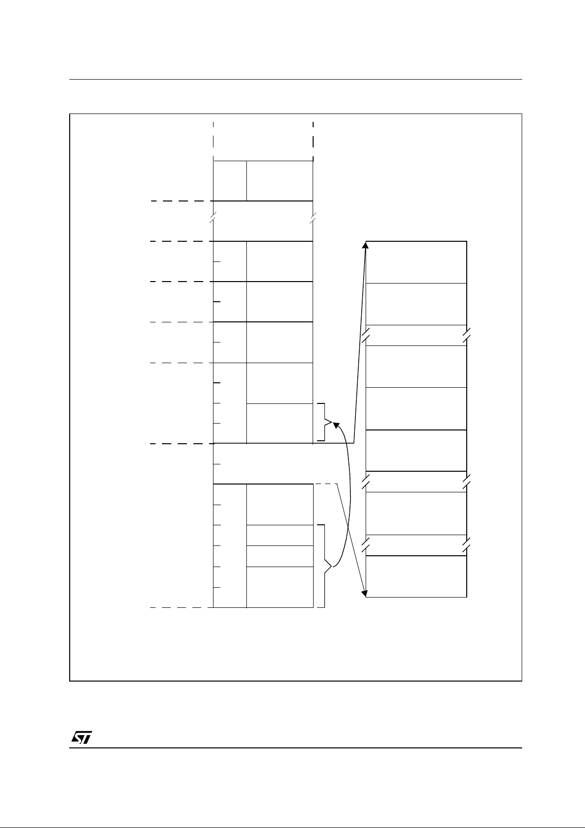
4 - MEMOR Y ORGA NI ZA T IO N
The memory space of the ST10F280 is configured
in a unified memory architecture. Code memory,
data memory, registers and I/O ports are organized within the same linear address space of
16M Bytes. The entire memory space can be
accessed bytewise or wordwise. Particular portions of the on-chip memory have additionally
been made directly bit addressable.
FLASH: 512K Bytes of on-chip single voltage
FLASH memory.
IRAM: 2K Bytes of on-chip internal RAM
(dual-port) is provided as a storage for data, system stack, general purpose register banks and
code. The register bank can con sist of up to 16
wordwide (R0 to R15) and/or bytewide (RL0, RH0,
…, RL7, RH7) general purpose registers. Base
address is 00’F600h, upper address is 00’FDFFh.
XRAM: 16K Bytes of on-chip extension RAM (single port XRA M) is provided as a storage for data,
user stack and cod e. The X RA M is a s ingle bank,
connected to the internal XBUS and are accessed
like an external memory in 16-bit demultiplexed
bus-mode without waitstate or read/write delay
(50ns access at 40MHz CPU clock). Byte and
word access is allowed.
The XRAM address range is 00’8000h - 00’BFFFh
if enabled (XPEN set bit 2 of SYSCON register-,
and XRAMEN set bit 2 of XPERCON register-). If
bit XRAMEN or XPEN is cleared, then any access
in the address range 00 ’8000h 00’BFFFh will be
directed to external memory interface, using the
BUSCONx register corresponding to address
matching ADDRSELx register
As the XRAM appears like external memory, it
cannot be used for the ST10F280’s system stack
or register banks. The XRAM is not provided for
single bit storage and therefore is not bit addressable.
SFR/ESFR: 1024 bytes (2 * 512 bytes) of address
space is reserved for the special func tion register
areas. SFRs are wordwide registers which are
used for controlling and monitoring functions of
the different on-chip units.
CAN1: Address range 00’EF00h 00’EFFFh is
reserved for the CAN1 Module access. The CAN1
is enabled by setting XPEN bit 2 of the SYSCON
register and bit 0 of the new XPERCON register.
Accesses to the CAN Module use demultiplexed
addresses and a 16-bi t data bus (byte accesses
are possible). Two waitstates give an access time
of 100 ns at 40MHz CPU clock. No tristate waitstate is used.
CAN2: Address range 00’EE00h 00’EEFFh is
reserved for the CAN2 Module access. The CAN2
is enabled by setting XPEN bit 2 of the SYSCON
register and bit 1 of the new XPERCON register.
Accesses to the CAN Module use demultiplexed
addresses and a 16-bi t data bus (byte accesses
are possible). Two waitstates give an access time
of 100 ns at 40MHz CPU clock. No tristate waitstate is used.
In order to meet the needs of designs where more
memory is required than is provided on chip, up to
16M Bytes of external RAM and/or ROM can be
connected to the microc ontroller. If one or the two
CAN modules are used, Port 4 can not be programmed to output all 8 segment address lines.
Thus, only 4 segment address li nes can be used,
reducing the external mem or y space to 5M Bytes
(1M Byte per CS
line).
XPWM: Address range 00’EC00h 00’ECFFh is
reserved for the XPWM Module access. The
XPWM is enabled by setting XPEN bit 2 of the
SYSCON register and bit 4 of the new XPERCON
register. Accesses to the XPWM Module use
demultiplexed addresses and a 16-bit data bus
(byte accesses are possible). Two waitstates give
an access time of 100 ns at 40MHz CPU clock. No
tristate waitstate is used.
XPORT9, XTIMER, XPORT10, XADCMUX :
Address range 00’C000h 00’C3FFh is reserved
for the XPORT9, XPORT10, XTIMER and
XADCMUX peripherals access. The XPORT9,
XTIMER, XPORT10, XADCMUX are enabled by
setting XPEN bit 2 of the SYSCON register and
the bit 3 of the new XPERCON register. Accesses
to the XPORT9, XTIMER, XPORT10 and
XADCMUX modules use a 16-bit demultiplexed
bus mode without waitstate or read/write delay
(50ns access at 40MHz CPU clock). Byte and
word access is allowed.
Visibi lity of X B U S Periphera ls
The XBUS peripherals can be separately selected
for being visible to the user by means of corresponding selection bits in the XP E RCON re gister.
If not selected (not activated with XPERCON bit)
before the global enabling with XPEN-bit in
SYSCON register, the corresponding address
space, port pins and interrupts are not occupied
by the peripheral, thus the peripheral is not visible
and not available. SYSCON register is described
in Section 19.2 - System Configuration Registers.
ST10F280
19/186
Figure 4 : ST10F280 On-chip Memo ry Mapping
14
07
06
05
04
00’4000
01
00
00’0000
02
00’C000
00’FFFF
SFR : 512 Bytes
00’FE00
00’FDFF
IRAM : 2K Bytes
00’F600
* Blocks 0, 1 and 2 may be remapped from segment 0 to segment 1 by setting SYSCON-ROMS1 (before EINIT)
RAM, SFR and X-pheripherals are
mapped into the address space.
Segment 4Segment 3Segment 2Segment 1Segment 0
Data
Page
Number
Absolute
Memory
Address
00’6000
00’F1FF
ESFR : 512 Bytes
00’F000
00’EFFF
CAN1 : 256 Byte s
00’EF00
00’EEFF
CAN2 : 256 Byte s
00’EE00
00’C3FF
XPORT9 XTIMER
00’C000
03
00’ECFF
XPWM
00’EC00
Block2 = 8K Bytes
Internal
Flash
Memory
Block1 = 8K Bytes
Block0 = 16K Bytes
01’0000
01’8000
02’0000
03’0000
0C
04’0000
10
05’0000
Block6 = 64K Bytes
Block5 = 64K Bytes
Block4 = 64K Bytes
Block3 = 32K Bytes
Block2*
Block1*
Block0*
Data Page Number and A bsolute Memory Address are hexadecim al values.
08
08’0000
20
Block10 = 64K Bytes
Segment 8
09’0000
00’8000
00’BFFF
XRAM = 16K Bytes
XPORT10
XADCMUX

ST10F280
20/186
XPERCON (F024h / 12h) ESFR Reset Value: - - 05h
Note: - When both CAN and XPWM are disabled via XPERCON setting, then any access in the address
range 00’EC00h 00’EF FFh will be directed to external mem ory interface, using the BUSCONx
register corresponding to address matching ADDRSELx register. P4.4 and P4.7 can be used as
General Purpo se I/O when CAN2 is no t enabled, and P4.5 and P4. 6 can be used as G eneral
Purpose I/O when CAN1 is not enabled.
- The default XPER selection after Reset is : XCAN1 is enabled, XCAN2 is disabled, XRAM is
enabled, XPORT9, XTIMER, XPORT10, XPWM, XADCMUX are disabled.
- Register XPERCON cannot be changed after the global enabling of XPeripherals, i.e. after
setting of bit XPEN in SYSCON register.
15141312111098765 4 3 2 1 0
-----------XPWMENXPERCONEN3XRAMENCAN2ENCAN1EN
RW RW RW RW RW
Bit Function
CAN1EN
0
1
CAN1 Enable Bit
Accesses to the on- chip CAN 1 XPeripheral a nd its fu nctions are disabled. P4.5 a nd P4.6 pins
can be used as gen eral purpose I/Os. Addre ss range 00’EF00h-00’EF FFh is only directed to
external memory if CAN2EN and XPWM bits are cleared also.
The on-chip CAN1 XPeripheral is enabled and can be accessed.
CAN2EN
0
1
CAN2 Enable Bit
Accesses to the on- chip CAN 2 XPeripheral a nd its fu nctions are disabled. P4.4 a nd P4.7 pins
can be us ed as gene ral purpos e I/Os. Addres s range 00’E E00h-00’EEFFh is only di rected to
external memory if CAN1EN and XPWM bits are cleared also.
The on-chip CAN2 XPeripheral is enabled and can be accessed.
XRAMEN
0
1
XRAM Enable Bit
Accesses to the on-chip 16K Byte XRAM are disabled, external access performed.
The on-chip 16K Byte XRAM is enabled and can be accessed.
XPERCONEN3
0
1
XPORT9, XTIMER, XPORT10, XADCMUX Enable Bit
Accesses to the XPORT9, XTIMER, X PORT10, XADCMUX p eripherals are d isabled, external
access performed.
The on-chip XPORT9, XTIMER, XPORT10, XADCMUX peripherals are enabled and can be
accessed.
XPWMEN
0
1
XPWM Enable Bit
Accesses to the on-chip XPWM are disabled, external access performed. Address range
00’EC00h-00’ECFFh is only directed to external memory if CAN1EN and CAN2EN are ‘0’ also
The on-chip XPWM is enabled and can be accessed.

ST10F280
21/186
5 - INTERNAL FLASH MEMORY
5.1 - Overview
– 512K Byte on-chip Flash memory
– Two possibilities of Flash mapping into the CPU
address space
– Flash memory can be used for code and data
storage
– 32-bit, zero waitstate read ac cess (50ns cycle
time at f
CPU
= 40MHz)
– Erase-Program Controller (EPC) similar to
M29F400B STM’s stand-alone Flash memo ry
• Word-by-Word Programmable (16µs t ypic a l)
• Data polling and Toggle Protocol for EPC
Status
• Internal Power-On detection circuit
– Memory Erase in blocks
• One 16K Byte, two 8K Byte, one 32K Byte,
seven 64K Byte blocks
• Each block can be erased separately
(1.5 second typical)
• Chip erase (8.5 second typical)
• Each block can be separately protected
against programming and erasing
• Each protected block can be temporary unprotected
• When enabled, the read protection prevents
access to data in Flash memory using a program running out of the Flash memory space.
Access to data of internal Flash can only be performed with an inner protected program
– Erase Suspend and Res um e Modes
• Read and Program another Block during erase
suspend
– Single Voltage operat ion , no need of dedicat ed
supply pin
– Low Power Consumption:
• 45mA max. Read current
• 60mA max. Program or Erase current
• Automatic Stand-by-mode (50µA maximum)
– 100,000 Erase-Program Cycles per block,
20 y ea r data reten tion time
– Operating tempe rature: -40 to +125
o
C
5.2 - Operational Overview
Read M ode
In standard mode (the normal operating mode)
the Flash ap pears like an on-chip ROM with the
same timing and functiona lity. The Flash modul e
offers a fast access time, allowing zero waitstate
access with CPU frequency up to 40MHz.
Instruction fetches and data operand reads are
performed with all addressing modes of the
ST10F280 instruction set.
In order to optimize the programming tim e of the
internal Flash, blocks of 8K Bytes, 16K Bytes,
32K Bytes, 64K Bytes can be used. But the size of
the blocks does not apply to the whole memory
space, see details in Table 2.
Table 2 : 512K Byte Flash Memory Block Organisation
Block Addresses (Segment 0) Addresses (Segment 1) Size (K Byte)
0
1
2
3
4
5
6
7
8
9
10
00’0000h to 00’3FFFh
00’4000h to 00’5FFFh
00’6000h to 00’7FFFh
01’8000h to 01’FFFFh
02’0000h to 02’FFFFh
03’0000h to 03’FFFFh
04’0000h to 04’FFFFh
05’0000h to 05’FFFFh
06’0000h to 06’FFFFh
07’0000h to 07’FFFFh
08’0000h to 08’FFFFh
01’0000h to 01’3FFFh
01’4000h to 01’5FFFh
01’6000h to 01’7FFFh
01’8000h to 01’FFFFh
02’0000h to 02’FFFFh
03’0000h to 03’FFFFh
04’0000h to 04’FFFFh
05’0000h to 05’FFFFh
06’0000h to 06’FFFFh
07’0000h to 07’FFFFh
08’0000h to 08’FFFFh
16
8
8
32
64
64
64
64
64
64
64

ST10F280
22/186
Instructions and Commands
All operations besides normal read operations are
initiated and controlled by command sequences
wri tte n to the Fla sh C om ma n d I nter fac e ( CI) . T h e
Command Interface (CI) interprets words written
to the Flash memory and enables one of the
following operations:
– Read memory array
– Program Word
– Block Erase
– Chip Erase
– Erase Suspend
– Erase Resume
– Block Protection
– Block Temporary Unprotection
– Code Protection
Commands are composed o f several write cycles
at specific addresses of the Flash memory. The
different write cycles of such command
sequences offer a fail-safe feature to protect
against an inadvertent write.
A command only starts when the Command
Interface has decoded the last write cycle of an
operation. Until that last write is performed, Flas h
memory rema ins in Read Mo de
Notes: 1. As it is not possible to perform write
operations in the Flash while fetching code
from Flash, the Flash commands must be
written by instructions executed from
internal RAM or ex ternal memo ry.
2. Command write c ycles do not need to
be consecutively received, pauses are
allowed, save for Block Erase command.
During this operation all Erase Confirm
commands mus t be sent to co mplete any
block erase operation before time-out
period expires (typically 96µs). Command
sequencing must be followed exactly. Any
invalid combination of commands will reset
the Command Interface to Read Mode.
Status R egister
This register is used to flag the status of the
memory and the result of an operation. This
register can be accessed by read cycles during
the Erase-Program Controller (EPC) operation.
Erase Operation
This Flash memory features a block erase
architecture with a chip erase capabi lity too. Erase
is accomplished by exec uting the six cycle erase
command sequence. Additional command write
cycles can then be performed to erase more than
one block in parallel . When a time-out period elaps
(96
µ
s) after the last cycle, the Erase-Program
Controller (EPC) automatically starts and times the
erase pulse and executes the erase operation.
There is no need to program the block to be
erased with ‘0000h’ before an erase operation.
Term ination of operation is indicated in the Flash
status register. After erase operation, the Flash
memory locations are read as 'FFFFh’ value.
Erase Suspend
A block erase operation is typically executed
within 1.5 second for a 64K Byte block. Erasure of
a memory block may be suspended, in order to
read data from another block or to program data in
another block, and then resumed.
In-System Programming
In-system programming is fully supported. No
special programming voltage is required. Because
of the automatic execution of erase and
programming algorithms, write operations are
reduced to transferring commands and data to the
Flash and reading the status. Any code that
programs or erases Flash memory lo cations (that
writes data to the Flash) must be executed from
memory out side the on-chip Flash memory its elf
(on-chip RAM or external memory).
A boot mechanism is provided to support
in-system programming. It wor ks using seria l link
via USART interface and a PC compatible or
other programming host.
Read/Write Protection
The Flash module supports read and write
protection in a very comfortable and advanced
protection functionality. If Read Protection is
installed, the whole Flash memory is protected
against any "external" read access; read
accesses are only possible with instructions
fetched directly from program Flash memory. For
update of the Flas h memor y a temporar y disable
of Flash Read Protection is supported.
The device also features a block write protection.
Software locking of selectable memory blocks is
provided to protect code and data. This feature
will disable both program and erase operations in
the selected block(s) of the memory. Block
Protection is accomplished by block specific
lock-bit which are programmed by executing a
four cycle command sequence. The locked state
of blocks is indicated by specific flags in the
according block status registers. A block may only
be temporarily unlocked for update (write)
operations.

ST10F280
23/186
With the two possibilities for write protection whole
memory or block specific a flexible installation of
write protection is suppor ted to protect the Flash
memory or parts of it from unauthorized
programming or erase accesses and to provide
virus-proof protection for all system code blocks.
All write protection also is enabled during boot
operation.
Power Supply, Reset
The Flash modul e uses a si ngle power supply for
both read and write functions. Internally generated and regulated voltages are provided for the
program and erase operations from 5V supply.
Once a program or erase cycle has been completed, the device resets to the standard read
mode. At power-on, the Flash memory has a
setup phase of some microseconds (dependent
on the power supply ramp-up). During this phase,
Flash can not be read. Thus, if EA
pin is high (execution will start from F lash m em or y ), the CP U will
remains in reset state until the Flash can be
accessed.
5.3 - Architectural Description
The Flash module distinguishes two basic
operating modes, the standard read mode and the
command mo de. The initial state after power-on
and after reset is the standard read mode.
5.3.1 - Read Mode
The Flash modul e enters the standard operating
mode, the read mode:
– After Reset command
– After every completed erase operation
– After every completed programming operation
– After every other completed command
execution
– Few microseconds after a CPU-reset has
started
– After incorrect address and data values of
command sequences or writing them in an
improper sequence
– After incorrect write access to a read protected
Flash memory
The read mode remains active until the last
command of a command sequence is decoded
which starts directly a Flash array operation, such
as:
– erase one or several blocks
– program a word into Flash array
– protect / temporary unprotect a block.
In the standard read mode read accesses are
directly controlled by the Flash memory array,
delivering a 32-bit double Word from the
addressed position. Read accesses are always
aligned to double Word boundaries. Thus, both
low order address bit A1 and A 0 are not used in
the Flash array for read accesses. The high order
address bit A18/A17/A16 define the physical
64K Bytes segment being accessed within the
Flash array.
5.3.2 - Command Mode
Every operation besides standard read operations
is initiated by commands written to the Flash
command register. The addresses used for
command cycles define in conjunction with the
actual state the specific step within command
sequences. With the last command of a command
sequence, the Erase-Program Controller (EPC)
starts the execution of the command. The EPC
status is indicated during comman d execution by:
– The Status Register,
– The Ready/Bu sy signal.
5.3.3 - Flash Status Register
The Flash Status register is used to flag the status
of the Flash memory and the result of an
operation. This register can be accessed by Read
cycles during the program-Erase Controller
operations. The program or erase operation can
be controlled by data polling on bit FSB.7 of
Status Register, detection of Toggle on FSB.6 and
FSB.2, or Error on FSB.5 and Erase Timeout on
FSB.3 bit. Any read attempt i n Flash during E PC
operation will a utomatic ally ou tput thes e five bits.
The EPC sets bit FSB.2, FSB.3, FSB.5, FSB.6
and FSB.7. Other bit are reserved for future use
and should be masked.

ST10F280
24/186
Flash Status (see note for address)
Note: The Address of Flash Status Register is the address of the word being programmed when
Programming operation is in progress, or an address w ithin block being erased when Erasing
operation is in progress.
15 14 13 12 11 10 9 8 7 6 5 4 3 2 1 0
-------- FSB.7 FSB.6 FSB.5 - FSB.3 FSB.2 - RRR R R
FSB.7 Flash Status bit 7: Data Polling Bit
Programming Operation: this bit outputs the complement of the bit 7 of the word being
programm ed , and after com ple t ion , w ill ou t pu t the b it 7 of the wo rd progr ammed.
Erasing Operation: outputs a ‘0’ during erasing, and ‘1’ after erasing completion.
If the block selected f or erasure is (are) protected, FSB.7 will be set to ‘0’ for about 100 µs, and
then return to the previous addressed memory data value.
FSB.7 will also flag t he Erase Suspend Mode by switching from ‘0’ to ‘1’ at the star t of the
Erase Suspend.
During Program operation in Erase Suspend Mode, FSB.7 will have the same behaviour as in
normal Program execution outside the Suspend mode.
FSB.6 Fl ash S t at us bit 6: Toggle Bit
Programming or Erasing Operations: successive read operations of Flash Status register will
deliver complementary values. FSB.6 will togg le each time the Flash Status register is read.
The Program operation is completed wh en two successive reads yield the same value. The
next read will output the bit last programmed, or a ‘1’ after Erase operation
FSB.6 will be set to‘1’ if a read operation is attempted on an Erase Suspended block. In
addition, an Erase Suspend/Resume command will cause FSB.6 to toggle.
FSB.5 Flash Status bit 5: Error Bit
This bit is set to ‘1’ when there is a failure of Program, block or chip erase operations.This bit
will also be set if a user tries to program a bit to ‘1’ to a Flash location that is currently
programmed with ‘0’.
The error bit resets after Read/Reset instruction.
In case of success, the Error bit w il l be set to ‘0’ during Program or Erase and then w ill o utpu t
the bit last programmed or a ‘1’ after erasing
FSB.3 Flash Status bit 3: Erase Time-out Bit
This bit is cleared by the EPC when the las t Block Erase command has been en tered to the
Command Interface and it is awaiting the Erase start. When the time-out period is finished,
after 96 µs, FSB.3 returns back to ‘1’.
FSB.2 Fl ash S t at us bit 2: Toggle Bit
This toggle bit, together with FSB.6, can be used to determine the chip status during the Erase
Mode or Erase Suspend Mode. It can be used also to identify the block being Erased
Suspended. A Read operation will cause FS B.2 to Toggle during the Erase Mode. If the Flash
is in Erase Suspend Mode, a Read operation from the Erase suspen ded block or a Program
operation into the Erase suspended block will cause FSB.2 to toggle.
When the Flash is in Program Mode during Erase Suspend, FSB.2 will be read as ‘1’ if address
used is the address of the word being programmed.
After Erase completion with an Error status, FSB.2 will toggle when reading the faulty sector.

ST10F280
25/186
5.3.4 - Flash Protection Register
The Flash Protection register is a non-volatile register that contains the protection status. This register
can be read by using the Read Protection St atus (RP) command, and programmed by using the de dicated Set Protection command.
Flash Protection Register (PR)
5.3.5 - Instructions Description
Twelve instructions dedicated to Flash memory
accesses are defined as follow:
Read/Reset (RD). The Read/Reset instruction
consist of one write cycle with data XXF0h . it can
be optionally preceded by two CI enable
coded
cycles (data xxA8h at address 1554h + data
xx54h at address 2AA8h). Any successive read
cycle following a Read/Reset instruction will read
the memory array. A Wait cycle of 10µs is
necessary after a Read/Reset command if the
memory was in program or Erase mode.
Program Word (PW). This instruction uses four
write cycles. After the two Cl enable coded cycles ,
the Program Word command xxA 0h is written at
address 1554h. The following write cycle will latch
the address and data of the word to be
programmed. Memor y p rogramming can be do ne
only by writing 0's instead of 1's, otherwise an
error occurs. During programming, the Flash
Status is checked by reading the Flash Status bit
FSB.2, FSB.5, FSB.6 and FSB.7 which show the
status of the EPC. FSB.2, FSB.6 and FSB.7
determine if programming is on going or has
completed, and FSB.5 allows a check to be made
for any possible error .
Block Erase (BE). This instruction uses a
minimum of six command cycles. The erase
enable command xx80h is written at address
1554h after the two-cycle CI enable sequence.
The erase confirm code xx30h must be written at
an address related to the block to be erased
preceded by the execution of a second CI enable
sequence. Additional erase confirm codes must
be given to erase m ore than on e block in parallel.
Additional erase confirm commands must be
written within a defined time-ou t perio d. The input
of a new Block Erase command will restart the
time -out period.
When this time-out period has elapsed, the erase
starts. The status of the internal timer can be
monitored through the level of FSB.3, if FSB.3 is
‘0’, the Block Erase command has been given and
the timeout is running ; if FSB.3 is ‘1’, the timeout
has expired and the EPC is erasing the block(s).
If the second command given is not an erase confirm or if the coded cycles are wrong, the instruction aborts, and the device is reset to Read Mode.
1514131211109876543 210
CP ----BP10 BP9 BP8 BP7 BP6 BP5 BP4 BP3 BP2 BP1 BP0
RW RW RW RW RW RW RW RW RW RW RW RW
BPx Block x Protection bit (x = 0...10)
‘0’: the Block Protection is enabled for block x. Programming or erasing the block is not
possible, unless a Block Temporary Unprotection command is issued.
1’: the Block Protection is disabled for block x.
Bit is ‘1’ by default, and can be programmed permanently to ‘0’ using the Set Protection
command but then cannot be set to ‘1’ again. It is therefore possible to temporally disable the
Block Protection using the Block Temporary Unprotection instruction.
CP Code Protection Bit
‘0’: the Flash Code Protection is enabled. Read accesses to the Flash for execution not
performed in the Flash itself are not allowed, the returned value will be 009Bh, whatever the
content of the Flash is.
1’: the Flash Code Protection is disabled: read accesses to the Flash from external or internal
RAM are allowed
Bit is ‘1’ by default, and can be programmed permanently to ‘0’ using the Set Protection
command but then cannot be set to ‘1’ again. It is therefore possible to temporarily disable the
Code Protection using the Code Temporary Unprotection instruction.

ST10F280
26/186
It is not necessary to program the block with
0000h as the EPC will do this automatically before
the erasing to FFFFh. Read operations after the
EPC has sta rted, output the Flash Status Register. During the execution of the erase by the EPC,
the device accepts only the Erase Suspend a nd
Read/Reset instructions. Data Polling bit FSB.7
returns ‘0’ while the erasure is in progress, and ‘1’
when it has completed. The To ggle bit FSB.2 and
FSB.6 toggle during the erase operation. They
stop when erase is completed. After completion,
the Error bit FSB.5 returns ‘1’ if there has been an
erase failure because erasure has not comp leted
even after the maximum number of erase cycles
have been executed by the EPC, in this case, it
will be necessary to input a Read/Reset to the
Command Interface in order to reset the EPC.
Chip Erase (CE). This instruction uses six write
cycles. The Erase Enable command xx80h, must
be written at address 1554h after CI-Enable
cycles. The Chip Erase command xx10h must be
given on the sixth cycle after a second C I-Enable
sequence. An error in command sequence will
reset the CI to Read mode. It is NOT necessary to
program the block with 0000h as the E PC will do
this automatically before the erasing to FFFFh.
Read operations after the EPC has star ted out put
the Flash Status Register. During the execution of
the erase by the EPC, Data Polling bit FSB.7
returns ‘0’ while the erasure is in progress, and ‘1’
when it has completed. The FSB.2 and FSB.6 bit
toggle during the erase operation. They stop when
erase is finished. The FSB.5 error bit returns "1" in
case of failure of the erase operation. The error
flag is set after the maximum number of erase
cycles have been executed by the EPC. In this
case, it will be necessary to input a Read/Reset to
the Command Interface in order to reset the EPC.
Erase Suspend (ES). This instruction can be
used to suspend a Block Erase operation by
giving the command xxB0h without any specific
address. No CI-Enable cycles is required. Erase
Suspend operation allows reading of data from
another block and/or the programming in another
block while erase is in progress. If this com mand
is given during the time-out period, it will terminate
the time-out period in addition to erase Suspend.
The Toggle Bit FSB.6, when monitored at an
address that belongs to the block being erased,
stops toggling when Erase Suspend Command is
effective, It happens between 0.1µs and 15µs
after the Erase Suspend Command has been
written. The Flash will then go in normal Read
Mode, and read from blocks not being erased is
valid, while read from block being erased will
output FSB.2 toggling. Dur ing a Suspend phase
the only instructions valid are Erase Resum e and
Program Word. A Read / Reset instruction d uring
Erase suspend wi ll definitely abor t th e Erase a nd
result in invalid data in the block being erased.
Erase Resume (ER). This instruction can be
given when the memory is in Erase Suspend
State. Erase can be resumed by writing the
command xx30h at any address without any
Cl-enable sequence.
Program during Erase Sus pend. The Program
Word instruction during Erase Suspend is allowed
only on blocks that are not Erase-suspended. This
instruction is the same than the Program Word
instruction.
Set Prote c t io n (SP). This instruction can be used
to enable both Block Protection (t o protect each
block independently from accidental Erasing-Programming Operation) and Code Protection (to
avoid code dump). The Set Protection Com mand
must be given after a s pecial CI-Prot ection Enab le
cycles (see instruction table). The following Write
cycle, will p rogr am the Prote cti on Register. T o pro tect the block x (x = 0 to 10), the data bit x must be
at ‘0’. To protect the code, bit 15 of the data must
be ‘0’. Enabling Block or Code Protecti on is per-
manent and can be cleared only by STM. Block
Temporary Unprotection and Code Temporary
Unprotection instructions are available to allow the
customer to update the code.
Note: 1. The new value programmed in
protect ion regis ter will onl y becom e active
after a reset.
2. Bit that are already at ’0’ in protec tion
register must be confirmed at ’0’ also in
data latched during the 4th cycle of set
protection command, otherwise an error
may occur.
Read Protection Status (RP). This instru ction is
used to read the Block Protection status and the
Code Protection status. To read the protection
register (see Table 3), the CI-Protection Enable
cycles must be executed followed by the
command xx90h at address x2A54h. The
following Read Cycles at any odd word address
will output the Block Protection Status. The Read/
Reset command xxF0h must be written to reset
the protection interface.
Note: After a modification of protection register
(using Set Protection command), the Read
Protection Status will return the new PR
value only after a reset.

ST10F280
27/186
Block Temporary Unprotection (BTU). This Instruction can be used to temporar y unprotect all the
blocks from Program / Erase protection. The Unprotection is disabled after a Reset cycle. The Block
Tem porary Unprotection command xxC1h must be given to enable Block Temporar y Unprotection. The
Command must be preceded by the CI-Protection Enable cycles and followed by the Read/Reset
command xxF0h.
Set Code Protection (SCP). This kind of protection allows the customer to protect the proprietar y code
written in Flash. If installed and active, Flash Code Protection prevents data operand accesses and
program branches into the on-chip Flash area from any location outside the Flash memory itself. Data
operand accesses and branches to Flash locations are only and exclusively allowed for instructions
executed from the Flash memory itself. Every read or jump to Flash performed from another memory (like
internal RAM, external me mory) while Code Protection is enabled, will give the opcode 009Bh related to
TRAP #00 illegal instruction. The CI-Protection Enable cycles must be sent to set the Code Protection. By
writing data 7FFFh at any odd word addre ss, the Code Protec ted status is stored in the Flash Pr otec tion
Register (PR). Protection is permanent and cannot be cleared by the user. It is possible to temporarily
disable the Code Protection using Code Te mpo rar y Unprot ection instr uc tion.
Note: Bits that are already at ’0’ in protection register must be confirmed at ’0’ also in data latched during
the 4th cycle of set protection command, otherwise an error may occur.
Code Temporary Unprotection (CTU). This instruction must be used to temporary disable Code
Protection. This instruction is effective only if executed from Flash memory space. To restore the
protection status, without using a reset, it i s necessar y to use a Code Temporary Protection instruction.
System reset will reset also the Code Tem porary Unprotected status. The Code Temporary Unprotection
command consists of the following write cycle:
MOV MEM, Rn ; This instruction MUST be executed from Flash memory space
Where MEM is an absolute address inside memor y space, Rn is a register loaded with data 0FFFFh.
Code Temporary Protection ( C TP). This instruction allows to restore Code Protection. This operation is
effective only if executed from Flash memory and is necessar y to restore the protection status after the
use of a Code Temporary Unprotection instruction.
The Code Tem porary Protection command consist s of the following write cycle:
MOV MEM, Rn ; This instruction MUST be executed from Flash memory space
Where MEM is an absolute address inside memor y space, Rn is a register loaded with data 0FFFBh.
Note that Code Temporary Unprotection instruc tion must be used when it is necessary to modify the
Flash with protected code (SCP), since the write/erase routines must be executed from a memory
external to Flash space. Usually, the write/erase routines, executed in RAM, ends w ith a retur n to Flash
space where a CTP instruction restore the protection.
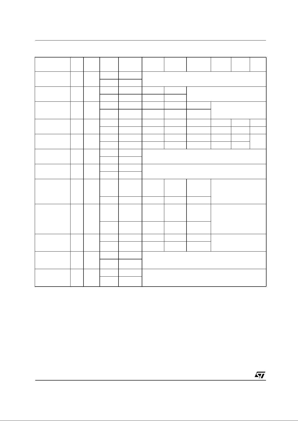
ST10F280
28/186
Table 3 : Instructions
Notes 1. Address bit A14, A15 and above are don’t care for coded add ress inputs.
2. X = Don’t Care.
3. WA = Write Address: addre ss of memory l ocation to be programmed.
4. WD = Write D ata: 16-bit data to be programmed
5. Optional , additi onal blocks addresses m ust be entered wi thin a ti m e-out delay (96 µs) after la st write entry, timeout st atus can be
verified th rough FSB.3 valu e. W hen full command is entered, read Dat a Poll i ng or Toggle bit unt i l Erase is compl et ed or suspended.
6. Read Data Polling or Tog gle bit until Erase completes.
7. WPR = W rite pro t ection regi ster. To protect code, bit 15 of WPR m ust be ‘0’. To protect blo ck N (N=0,1,.. .), bit N o f WPR must be
‘0’. Bit that are already at ‘0’ in protection register must also be ‘0’ in WPR, else a writing error will occurs (it is not possible to write a
‘1’ in a bit already programmed at ‘0’).
8. MEM = any add ress insid e the Fl ash m emor y s pace. Absolu te add ress ing m ode m ust be used (M OV MEM, Rn) , and ins tru cti on
must be executed from F l ash memory space.
9. Odd word address = 4n-2 w here n = 0, 1, 2, 3..., ex. 0002h, 0006h. ..
Instruction Mne Cycle
1
st
Cycle
2
nd
Cycle
3rd
Cycle
4th Cycle
5th
Cycle
6th
Cycle
7th
Cycle
Read/Reset RD 1+
Addr.
1
X
2
Read Memory Array until a new write cycle is initiated
Data xxF0h
Read/Reset RD 3+
Addr.
1
x1554h x2AA8h xxxxxh
Read Memory Array until a new write
cycle is initiated
Data xxA8h xx54h xxF0h
Program Word PW 4
Addr.
1
x1554h x2AA8h x1554h WA
3
Read Data Polling or
Toggle Bit until Program
completes.
Data xxA8h xx54h xxA0h WD
4
Block Erase BE 6
Addr.
1
x1554h x2AA8h x1554h x1554h x2AA8h BA BA’
5
Data xxA8h xx54h xx80h xxA8h xx54h xx30h xx30h
Chip Erase CE 6
Addr.
1
x1554h x2AA8h x1554h x1554h x2AA8h x1554h
Note
6
Data xxA8h xx54h xx80h xxA8h xx54h xx10h
Erase Suspend ES 1
Addr.
1
X
2
Read until Toggle stops, then read or program all data needed
from block(s) not being erased then Resume Erase.
Data xxB0h
Erase Resume ER 1
Addr.
1
X
2
Read Data Polling or Toggle bit until Erase completes or Erase
is supended another time.
Data xx30h
Set Block/Code
Protection
SP 4
Addr.
1
x2A54h x15A8h x2A54h Any odd
word
address
9
Data xxA8h xx54h xxC0h WPR
7
Read
Protection
Status
RP 4
Addr.
1
x2A54h x15A8h x2A54h Any odd
word
address
9
Read Protection Register
until a new write cycle is
initiated.
Data xxA8h xx54h xx90h Read
PR
Block
Temporary
Unprotection
BTU 4
Addr.
1
x2A54h x15A8h x2A54h X
2
Data xxA8h xx54h xxC1h xxF0h
Code
Temporary
Unprotection
CTU 1
Addr.
1
MEM
8
Write cycles must be executed from Flash.
Data FFFFh
Code
Temporary
Protection
CTP 1
Addr.
1
MEM
8
Write cycles must be executed from Flash.
Data FFFBh

ST10F280
29/186
– Generally, command sequences cannot be
written to Flash by instructions fetched from the
Flash itself. Thus, the Flash commands must be
written by instructions, executed from internal
RAM or external memory.
– Command cycles on the CPU interface need not
to be consecutively recei ved (pauses allowed).
The CPU interface delivers dummy read data for
not used cycles within command sequences.
– All addresses of command cycles shall be
defined only with Register-indirect addressing
mode in the according move instructi o ns. Di re ct
addressing is not allowed for command
sequences. Address segment or data page
pointer are taken into account for the com mand
address value.
5.3.6 - Reset Processing and Initial State
The Flash module distinguishes two kinds of CPU
reset types
The lengthening of CPU reset:
– Is not reported to external devices by
bidirectional pin
– Is not enabled in case of external start of CPU
after reset.
5.4 - Flash Memory Configuration
The default memory configuration of the
ST10F280 Memor y is determined by the state of
the EA
pin at reset. This value is stored in the
Internal ROM Enable bit (named ROMEN) of the
SYSCON register.
When ROMEN = 0, the interna l Flash is disabled
and external ROM is used for startup control.
Flash memor y can la ter be enabled by setting the
ROMEN bit of SYSCON to 1. The code
performing this setting must not run from a
segment of the extern al ROM to be replaced by a
segment of the Flash memory, otherwise
unexpected behaviour may occur.
For example, if external ROM code is located in
the first 32K Bytes of segment 0, the first
32K Bytes of the Flash must then be enabled in
segment 1. This is done by setting the ROMS1 bit
of SYSCON to 0 before or simultaneously with
setting of ROMEN bit. This must be done in the
externally supplied program before the execution
of th e EINI T inst ruction.
If program execution starts from external memory,
but access to the Flash memory mapped in
segment 0 is later required, then the code that
performs the setting of ROMEN bit must be
executed either in the segment 0 but above
address 00’8000h, or from the internal RAM.
Bit ROMS1 only affects the mapping of the first
32K Bytes of t he Flash memor y. All other par t s of
the Flash memory (addresses 01’8000h
08’FFFFh) remain unaffected.
The SGTDIS Segmentation Disable / Enable must
also be set to 0 to allow the use of the full
512K Bytes of on-c hip memory i n addition to the
external boot memor y. The correct procedure on
changing the segmentation registers must also be
observed to prevent an unwanted trap condition:
– Instructions that configure the internal mem ory
must only be executed from external memory or
from the internal RAM.
– An Absolute Inter-Segment Jump (JMPS)
instruction must be executed after Flash
enabling, to the next instruction, even if this next
instruction is located in the consecutive address.
– Whenever the internal Memory is disabled,
enabled or remapped, the DPPs must be
explicitly (re)loaded to enable correct data
accesses to the internal memory and/or external
memory.
5.5 - Application Examples
5.5.1 - Handling of Flash Addresses
All command, Block, Data and register addresses
to the Flash have to be located w ithin the active
Flash memory space. The active space is that
address range to which the physical Flash
addresses are mapped as defined by the user.
When using data page pointer (DPP) for block
addresses make sure that address bit A15 and
A14 of the block address are reflected in both
LSBs of the selected DPPS.
Note: - For Command Instructions, address bit
A14, A15, A16, A17 and A18 are don’t
care. This simplify a lot the application
software, because it minimize the use of
DPP registers when using Command in
the Command Interface.
- Direct addressing is not allowed for
Command sequence operations to the
Flash. Only Register-indirect addressing
can be used for command, block or
write-data accesses.

ST10F280
30/186
5.5.2 - Basic Flash Access Control
When accessing the Flash all command write addresses have to be located within the active Flash
memory s pace. The active Flash memor y space is that logical address range which is covered by the
Flash after mapping. When using data page pointer (DPP) for addressing the Flash, make sure that
address bit A15 and A14 of the command addresses are reflected in both LSBs of the selected data page
pointer (A15 DPPx.1 and A14 DPPx.0).
In case of the command write addresses, address bit A14, A15 and above are don’t care. Thus, command
writes can be performed by only using one DPP register. This allow to have a more simple and com pact
application software.
Another advantageous possibility is to use the extended segment instruction for addressing.
Note: The direct addressing mode is not allowed for write access to the Flash address/command
register. Be aware that the C compiler may use this kind of addressing. For write accesses to
Flash module always the indirect addressing mode has to be selected.
The following basic instruction sequences show examples for different addressing possibilities.
Principle example of address generation for Flash commands and registers:
When using data page pointer (DPP0 is this example)
MOV DPP0,#08h ;adjust data page pointers according to the
;addresses: DPP0 is used in this example, thus
;ADDRESS must have A14 and A15 bit set to ‘0’.
MOV Rw
m
,#ADDRESS ;ADDRESS could be a dedicated command sequence
;address 2AA8h, 1554h ... ) or the Flash write
;address
MOV Rw
n
,#DATA ;DATA could be a dedicated command sequence data
;(xxA0h,xx80h ... ) or data to be programmed
MOV [Rw
m
],Rw
n
;indirect addressing
When using the extended segment instruction:
MOV Rw
m
,#ADDRESS ;ADDRESS could be a dedicated command sequence
;address (2AA8h, 1554h ... ) or the Flash write
;address
MOV Rw
o
,#DATA ;DATA could be a dedicated command sequence data
;(xxA0h,xx80h ... ) or data to be programmed
MOV Rw
n
,#SEGMENT ;the value of SEGMENT represents the segment
;number and could be 0, 1, 2, 3 or 4 (depending
;on sector mapping) for 256KByte Flash.
EXTS Rw
n
,#LENGTH ;the value of Rwn determines the 8-bit segment
;valid for the corresponding data access for any
;long or indirect address in the following(s)
;instruction(s). LENGTH defines the number of
;the effected instruction(s) and has to be a value
;between 1...4
MOV [Rw
m
],Rw
o
;indirect addressing with segment number from
;EXTS
 Loading...