

13.56 MHz Short Range Contactless Memory Chip
176 bit USER EEPROM and 64-bit Unique ID
FEATURES SUMMARY
■ ISO 14443 - 2 Type B Air Interface Compliant
■ ISO 14443 - 3 Type B Frame Format Compliant
■ 13.56MHz Carrier Frequency
■ 847kHz Subcarrier Frequency
■ 106kbit/s Data Transfer
■ Data Transfer
– ASK Modulation from Reader to Tag
– BPSK Coding from Tag to Reader
■ 176-bit EEPROM with Write Protect Feature
■ 64-bit Unique Identifier
■ READ BLOCK & WRITE BLOCK (16 Bit s )
■ Internal Tuning Capacitor
■ Self-Tim e d P rogramming Cycle
■ 5ms Programming Time (typical)
■ More than 100,000 Erase/Write Cycles
■ More than 10 Year Data Retention
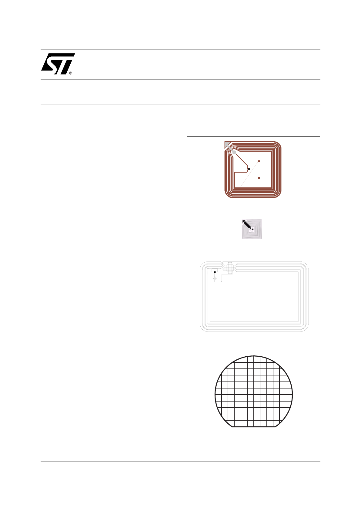
Figure 1. Delivery Forms
Antenna (
Antenna (A4)
SR176
DATA BRIEFING
A3)
2003
Complete data available under NDA.
Antenna (A5)
Wafer
1/5
SR176
SUMMARY DESCRIPTION
The SR176 is a contactless memory, powered by
an externally transm itted radio wave. It contains
176 bits of user EEPROM, fabricated with STMicroelectronics CMOS technology. The memo ry is
organized as 16 blocks of 16 bits, of which 11
blocks are user accessible.
The SR176 is accessed via the 13.56MHz carrier.
Incoming data are demodulated and decoded
from the received Amplitude Shift Keying modulation signal (ASK). The modula tion index of t his signal is 10%. Outgo ing data are generated by load
variation using Bit Phase Shift Keying (BPSK) of a
847kHz subcarrier. The Data transfer rate between the SR176 and the reader is 106kbit/s in
both reception and emission modes.
The SR176 follows the ISO 14443 pa rt 2 type B
recommendation for radio frequency power and
signal interface.
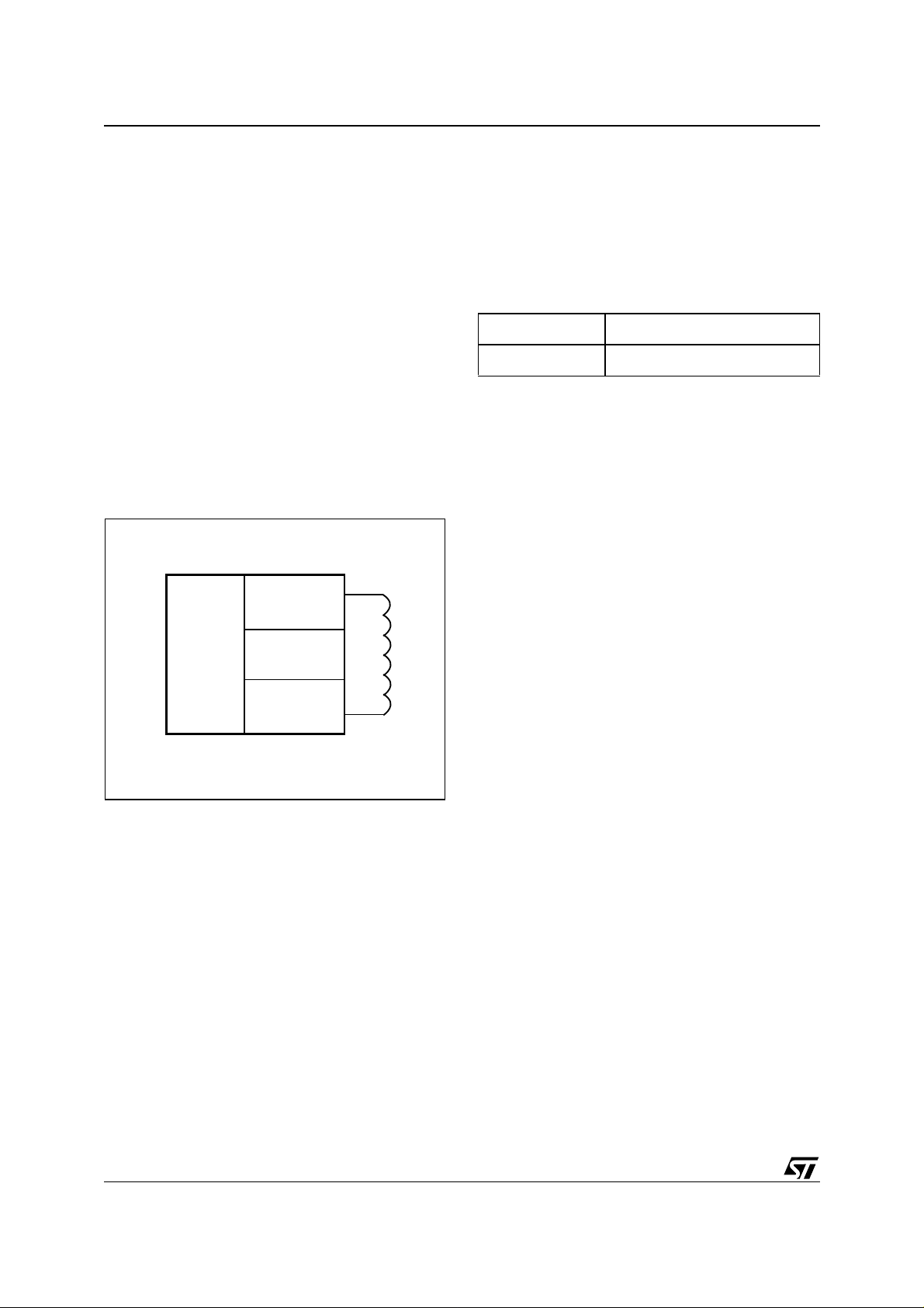
Figure 2. Logic Diagram
SR176
Power
Supply
Regulator
176 bit
User
EEPROM
ASK
Demodulator
BPSK
Load
Modulator
The SR176 is principally desi gned for s hort range
applications, such as in object identification, that
AC1
AC0
AI04995
need a low cost and non-reusable product. The
SR176 does not include any ant i-collis ion mec hanism, but does include a simple selection mechanism to cope with cases where more than one tag
is present, within the range of the Rea der, at the
any one time.
Table 1. Signal Names
AC1 Antenna Coil
AC0 Antenna Coil
The SR176 contactless EEPROM offers read and
write random access in block mode. One block is
composed by 16 bits . The device has an instruction set containing seven commands:
■ READ_BLOCK
■ WRITE_BLOCK
■ INITIATE
■ SELECT
■ COMPLETION
■ PROTECT_BLOCK
■ GET_PROTECTION.
The SR176 is divided into two major areas: the
unique identifier (UID) and the User EEPROM.
The UID is a 64 -bit uniq ue identifier written by ST
during product manufacturing. The User EEPROM
is divided into areas which c an be write-protected
so that they behave as ROM. The write protection
is activated using an OTP lo ck bits register. It is
possible to program the SR176 4-bit chip_ID used
by the SELECT command. Its default value is fixed
at the value 0 (0000
) by ST. When correctly s et,
b
up to sixteen SRIX4Ks can be selected individually.
2/5

MEMORY MAPP I N G
The SR176 is organized as 16 blocks of 16 bits, as
shown in Figure 3.
The firs t four blocks, from location 0 to 3, are u se d
to store read-only data. They store the 64-bit UID.
This value cannot be modified.
Blocks from locations 4 t o 14 offer a 176-bit EEPROM user area in which the application can store
Figure 3. SR176 Memory Mapp ing
SR176
its data values. Block 15 contains the OTP
LOCK_REG and the programmed Chip_ID.
The PROTECT_BLOCK comm and is used to lock
write access to blocks 4 to 15 by a group of 2
blocks.
The GET_PROTECTION command gives the status of the protection of blocks 4 to 15.
Block
Address
0
1
2
3
4
5
6
7
8
9
10
11
12
13
14
15
MSb LSb
b15
16-bit block
b7 b0b8
UID0
UID1
UID2
UID3
User Area
User Area
User Area
User Area
User Area
User Area
User Area
User Area
User Area
User Area
User Area
Chip_IDReservedOTP LOCK_REG
Description
64-bit UID
ROM
Lockable EEPROM
Lockable EEPROM
Lockable EEPROM
Lockable EEPROM
Lockable EEPROM
Lockable EEPROM
ai07699
3/5

SR176
PART NUMBERING
For a list of available options (speed, package,
etc.) or for further information on any aspect of this
Table 2. Ordering Information Scheme
Example: SR176 –W4/XXX
Device Type
SR176
Package
W4 =180µm ± 15µm Unsawn Wafer
SBN18= 180µm ± 15 µm Bumped and Sawn Wafer on 8-inch Frame
A3T= 38mm x 38mm Copper Antenna on Continuous Tape
A3S= 38mm x 38mm Copper Singulated Adhesive Antenna on Tape
A4T= 15mm x 15mm Copper Antenna on Continuous Tape
A4S= 15mm x 15mm Copper Singulated Adhesive Antenna on Tape
A5T= 42mm x 65mm Copper Antenna on Continuous Tape
A5S= 42mm x 65mm Copper Singulated Adhesive Antenna on Tape
Customer Code
XXX = Given by STMicroelectronics
device, please contact your nearest ST Sales O ffice.
4/5

SR176
Information furnished is believed to be accurate and reliable. However, STMicroelec tronics as sumes no responsibility for the consequences
of use of such information nor for any infringement of patents or other rights of third parties which may result from its use. No license is granted
by implic ation or o th erwise u nder any pat ent or pat ent righ ts of STMicroelectronics. Spec i fications m entioned i n this publication are subject
to change without notice. This publication supersedes and replaces all information previously supplied. STMicroelectronics products are not
authorized for use as c ritical components in li f e support dev i ces or systems without express writ ten approv al of STMicro el ectronics.
The ST log o i s registered trademark of STMic roelectronics
All other nam es are the property of th ei r respect ive owners
© July 2003 S T Microele ct ronics - All Rights Reserved
STMicroelectronics group of companies
Austra lia - Brazil - Canada - Chin a - Finland - Fr ance - Germa ny - Hong Kong -
India - Israel - Italy - Japan - Malaysia - Malta - Morocco - Singap ore - Spain - Sweden - Switz erland - Un ited Kingdo m - United St ates.
www.st.com
5/5
 Loading...