

SGS Thomson Microelectronics SMP50-100, SMP50-120, SMP50-130, SMP50-180, SMP50-200 Datasheet
...
®
TELECOM EQUIPMENT PROTECTION: TRISIL™
FEATURES
Bidirectional crowbar protection
■
Voltage range from 62V to 270V
■
Low capacitance from 15pF to 30pF typ.@ 50V
■
Low leakage current: IR= 2µA max.
■
Holding current: IH= 150 mA min.
■
Repetitive peak pulse current:
■
= 50 A (10/1000 µs)
I
PP
MAIN APPLICATIONS
Telecommunication equipment such as
Analog and digital line cards (xDSL, T1/E1,
■
ISDN...).
Terminals (phone, fax, modem...) and central
■
office equipment.
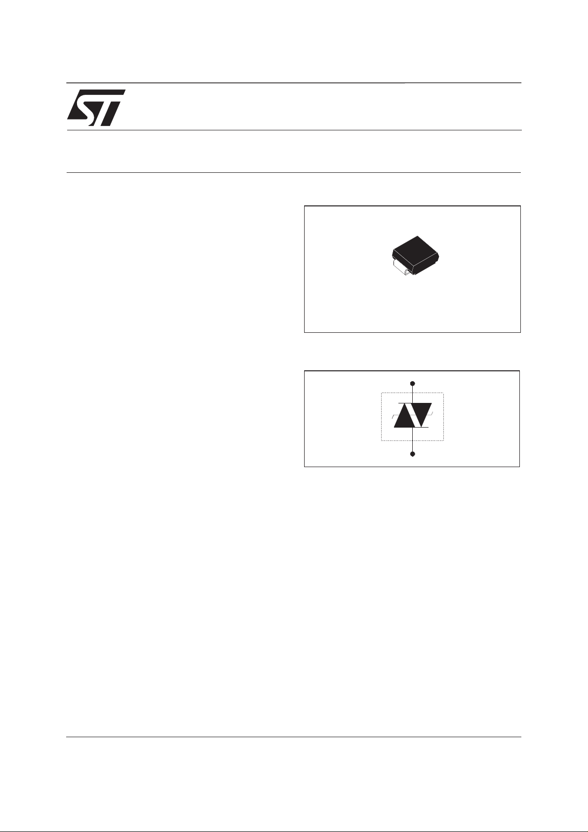
SMP50-xxx
SMA
(JEDEC DO-214AC)
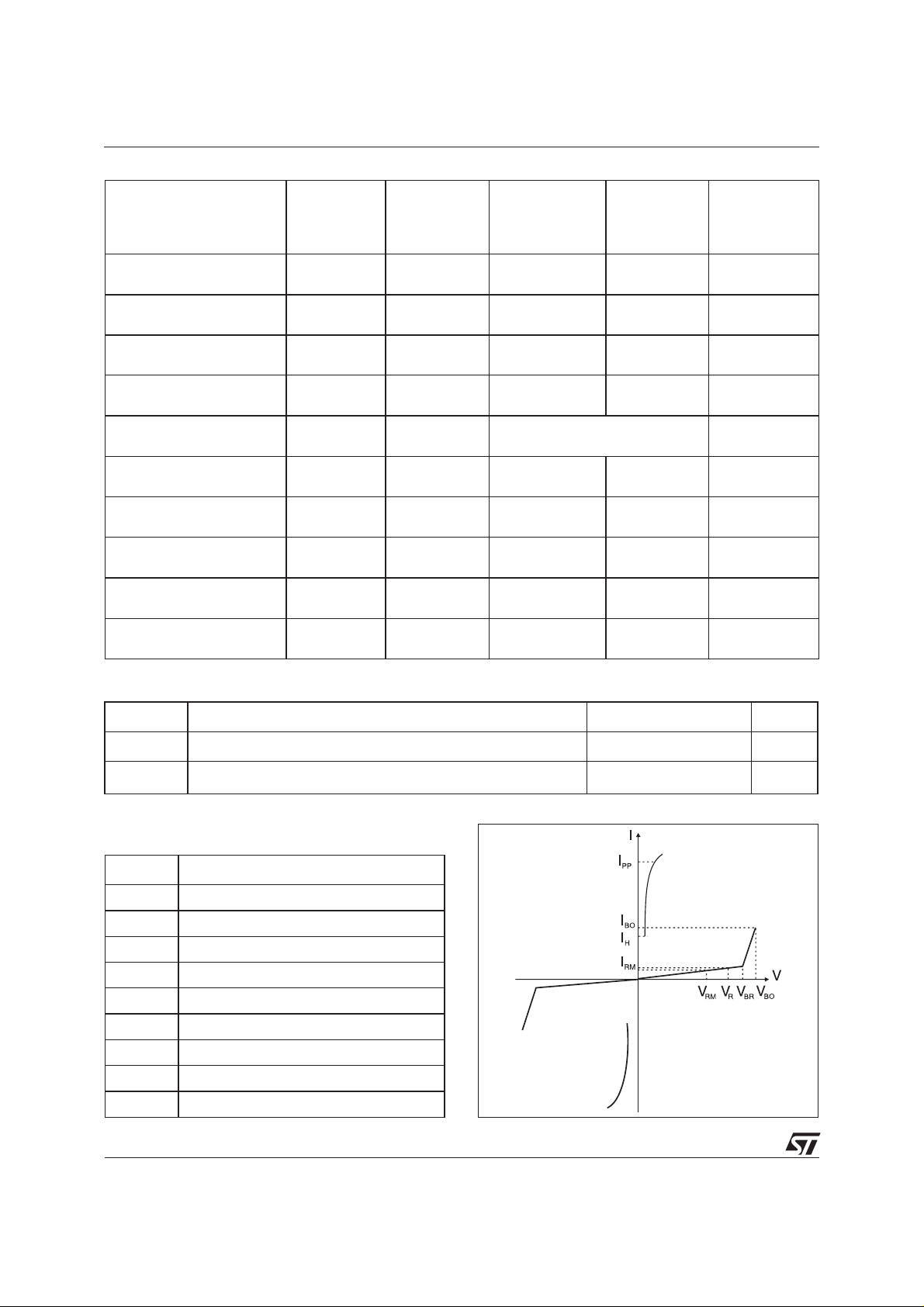
SCHEMATIC DIAGRAM
DESCRIPTION
The SMP50-xxx series has been designed to
protect telecommunication equipment against
lightningandtransientinduced byACpower lines.
The package/ die sizeratio has been optimizedby
using the SMA package.
BENEFITS
Trisils are not subject to ageing and provide a fail safe mode in short circuit for a better protection. Trisils
are used to help equipment to meet various standards such as UL1950, IEC950 / CSA C22.2, UL1459
and FCC part 68. Trisils have UL94 V0resinapproved.SMA package is JEDEC registred. (Trisils are UL
497B approved - file: E136224).
November 2002- Ed: 3B
1/8
SMP50-xxx
IN COMPLIANCES WITH THE FOLLOWING STANDARDS
Standard
GR-1089 Core
First level
GR-1089 Core
Second level
GR-1089 Core
Intra-building
ITU-T-K20 / K21
ITU-T-K20
(IEC61000-4-2)
VDE0433
VDE0878
IEC61000-4-5
FCC Part 68, lightning
surge type A
FCC Part 68, lightning
surge type B
Peak Surge
Voltage
(V)
2500
1000
Voltage
Waveform
(µs)
2/10
10/1000
Required peak
current (A)
500
100
Current
Waveform
(µs)
2/10
10/1000
5000 2/10 500 2/10 24
1500 2/10 100 2/10 0
6000
1500
6000
8000
4000
2000
4000
2000
4000
4000
1500
800
10/700
1/60 ns
10/700
1.2/50
10/700
1.2/50
10/160
10/560
150
37.5
5/310
ESD contact discharge
ESD air discharge
100
50
100
50
100
100
200
100
5/310
1/20
5/310
8/20
10/160
10/560
1000 9/720 25 5/320 0
Minimum
serial resistor
to meet
standard (Ω)
12
10
53
0
0
0
21.5
0
0
0
21.5
0
12.5
6.5
THERMAL RESISTANCES
Symbol Parameter Value Unit
R
(j-a)
th
(j-l)
R
th
Junction to ambient with recommended footprint
Junction to leads
120 °C/W
30 °C/W
ELECTRICAL CHARACTERISTICS
= 25°C)
(T
amb
Symbol Parameter
V
RM
I
RM
V
R
V
BR
V
BO
I
H
I
BO
I
PP
C
Stand-off voltage
Leakage current at V
RM
Continuous reverse voltage
Breakdown voltage
Breakover voltage
Holding current
Breakover current
Peak pulse current
Capacitance
2/8
SMP50-xxx
ABSOLUTE RATINGS (T
amb
= 25°C)
Symbol Parameter Value Unit
Repetitive peak pulse current:
I
I
I
TSM
I²t
T
T
T
PP
FS
stg
10/1000 µs
8/20 µs
10/560 µs
5/310 µs
10/160 µs
1/20 µs
2/10 µs
Fail safe mode: maximum current (note 1)
Non repetitive surge peak on-state current
(Sinusoidal)
8/20 µs 2.5 kA
t = 20ms
t = 16.6ms
t = 0.2s
t=2s
I²t value for fusing
t = 16.6ms
t = 20ms
L
Maximum lead temperature for soldering during 10 s.
Storage temperature range
j
Maximum junction temperature
50
100
55
65
75
100
150
25
28
16
8.5
6.5
6.3
260 °C
-55to+150
150
A
A
A²s
°C
°C
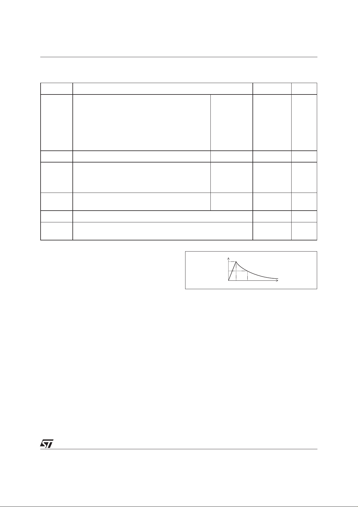
Repetitive peak pulse current
tr: rise time (µs)
tp: pulse duration time (µs)
ex: Pulse waveform 10/1000µs
tr = 10µs tp = 1000µs
100
%I
PP
50
0
t
t
p
r
t
3/8
 Loading...