

TRISIL
FEATURES
n Bidirectional crowbarprotection
n Low capacitance : C = 30 PF TYP @ 50V
n Low leakage current : I
n Repetitive peak pulse current :
IPP= 100 A (10/1000µS)
n Holding current: I
MAIN APPLICATIONS
Any sensitive equipment requiring protection
against lightning strikes and power crossing:
n Analog and digital line cards
(xDSL, T1/ E1, ISDN...)
n Gas tube replacement
n Terminals and transmission equipment
R
= 150 mA
H
=2µA MAX
SMP100LC-xxx
TM
FOR HIGH DEBIT RATE
TELECOM LINES PROTECTION
PRELIMINARY DATASHEET
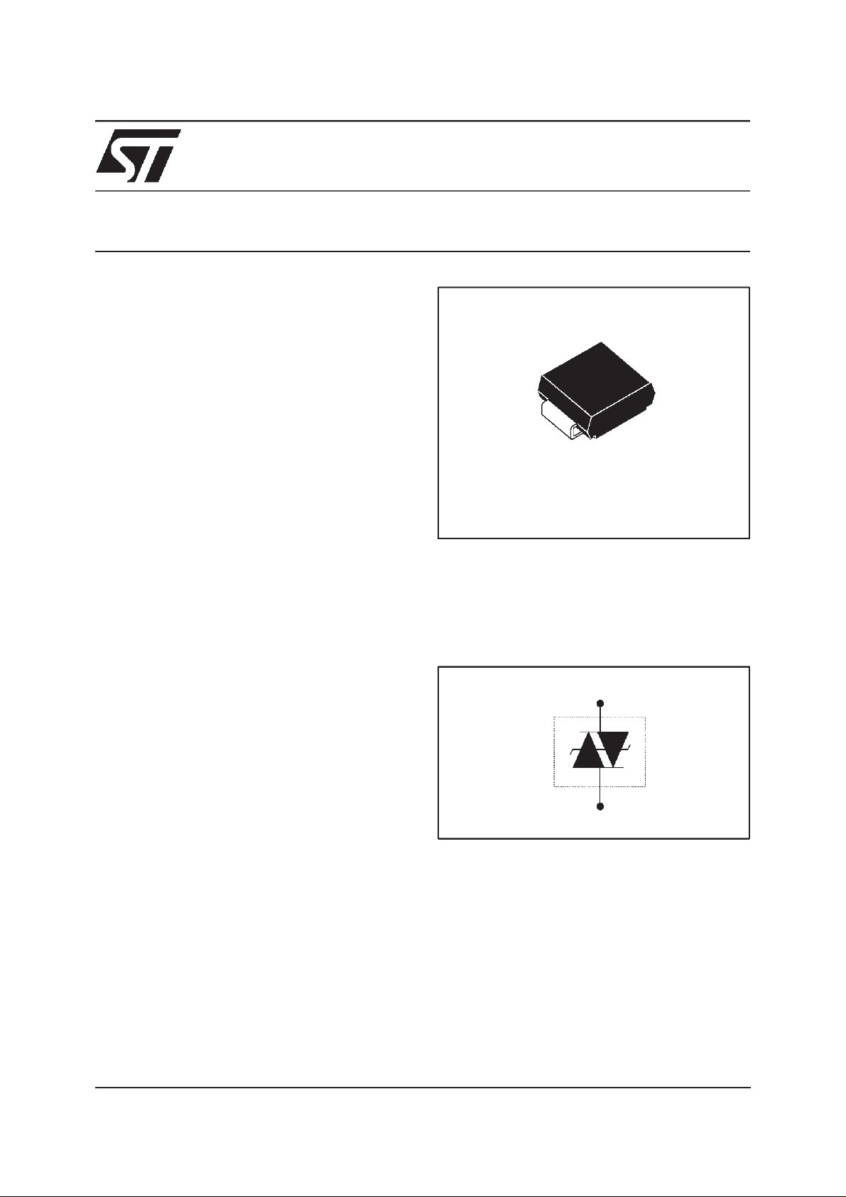
SMB
DESCRIPTION
The SMP100LC-x x x seri es is a very low
capac itance transient surge arrest or designed
for the protec tion of high debit rate
commun i c at ion equipment. It s low capac i t ance
avoid any dist orsion of t he signal. It can also
BENEFITS
n No ageing and no noise
n Short circuit in failure mode, thus still ensuring
protection
n Board space saving
SCHEMATIC DIAGRAM
March 2000 - Ed: 3B
1/8

SMP100LC-xxx
Necessary
Resistor
(note 1)
COMPLIES WITH THE
FOLLOWING STANDARDS:
Peak Surge
Voltage
(V)
Voltage
Waveform
(µs)
Current
Waveform
(µs)
Admissible
Ipp
(A)
ITU-T- K20 4000 10/700 5/310 100 VDE0433 4000 10/700 5/310 100 VDE0878 4000 1.2/50 1/20 100 IEC-1000-4-5 level 4
level 4
FCC Part 68,lightningsurge
type A
FCC Part 68,lightningsurge
1500
800
1000 5/320 5/320 25 -
10/700
1.2/50
10/160
10/560
5/310
8/20
10/160
10/560
100
100
200
100
type B
BELLCORE TR-NWT-001089
First level
BELLCORE TR-NWT-001089
2500
1000
2/10
10/1000
2/10
10/1000
500
100
5000 2/10 2/10 500 -
Second level
CNET I31-24
Note 1: minimum series resistanceto insert on the module line to withstandthe standard.
4000 0.5/700 0.8/310 100 -
THERMAL RESISTANCES
(Ω)
-
-
-
-
-
-
Symbol Parameter Value Unit
R
R
th(j-I)
th(j-a)
Junction to leads
Junction to ambient on printed circuit
20 °C/W
100 °C/W
(with standard footprint dimensions)
ABSOLUTE MAXIMUM RATINGS (T
= 25°C, unless otherwisespecified)
amb
Symbol Parameter Value Unit
I
pp
I
FS
I
TSM
T
L
T
stg
Tj
Note 2: infail safe mode, thedevice acts as a short circuit.
Repetitive peak pulse current:
10/1000 µs (open circuit voltage wave shape 1 kV 10/1000 µs)
8/20 µs (open circuit voltage wave shape 4 kV 1.2/50 µs)
5/310 µs (open circuit voltage wave shape 5 kV 10/700 µs)
2/10 µs (open circuit voltage wave shape 2.5 kV 2/10 µs)
100
250
150
500
Fail-safe mode : maximum current (note 2) 8/20 µs5kA
Non repetitive surgepeak on-statecurrent
One cycle
Non repetitive surgepeak on-statecurrent
F = 50Hz
50Hz
60Hz
0.2s
2s
50
53
23
10
Maximum lead temperature for soldering during 10s 260 °C
Storage temperature range
Maximum junction temperature
- 55 to + 150
150
A
A
A
A
A
A
A
A
°C
°C
2/8
SMP100LC-xxx
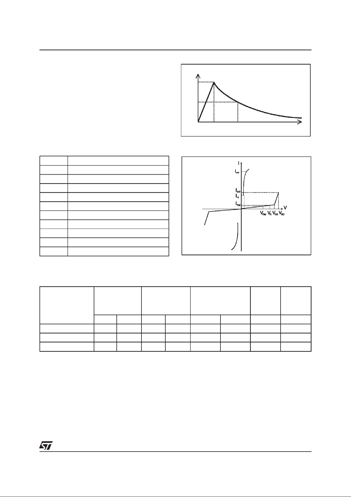
Pulse waveform:
10 / 1000 µstr=10µs tp = 1000 µs
8/20µstr=8µstp=20µs
5 / 310 µstr=5µs tp = 310 µs
1/20µstr=1µstp=20µs
2/10µstr=2µstp=10µs
ELECTRICALCHARACTERISTICS(T
Symbol Parameter
V
RM
I
RM
V
R
I
R
V
BR
V
BO
I
H
I
BO
I
PP
Stand-off voltage
Leakage current at V
RM
Continuous reverse voltage
Leakage current
Breakdown voltage
Breakover voltage
Holding current
Breakover current
Peak pulse current
C Capacitance
amb
=25°C)
%I
100
50
0
PP
t
rp
t
t
DYNAMIC PARAMETERS
Type
IRM@V
max.
RM
IR@V
max.
Note 1
R
VBO@I
BO
max.
Note 2
I
H
min.
Note 3
µAVµAV V mA mA pF
SMP100LC-140 2 120 50 140 185 800 150 30
SMP100LC-200 2 170 50 200 265 800 150 30
SMP100LC-270
Note 1: IRmeasured at VRguarantee VBR>V
Note 2: V
Note 3: See functional holding current testcircuit 1
Note 4: VR=50V bias, V
= 100V/µS, di/dt <10 A/µs, IPP= 100A
RISE
V
= 1kV/µS, di/dt < 10A/µs, IPP= 10A
RISE
VBOparameters are given by a KeyTek ”System2” generator withPN2461 module.
See test circuits 3for VBOdynamic parameters
2 230 50 262 350 800 150 30
R
=1V, F=1MHz.
RMS
C
typ.
Note 4
3/8
 Loading...