

Page 1
®
SMLVT3V3
FEATURES
UNIDIRECTIONAL TRANSIL DIODE
■
PEAK PULSE POWER : 600 W (10/1000µs)
■
REVERSE STAND-OFF VOLTAGE = 3.3 V
■
LOW CLAMPING FACTOR
■
FAST RESPONSE TIME
■
UL RECOGNIZED
■
DESCRIPTION
The SMLVT3V3 is a Transil diode designed
specifically for protecting 3.3V supplied sensitive
equipment against transient overvoltages.
Transil diodes provide high overvoltage protection
by clamping action. Their instantaneous response
to transient overvoltages makes then particularly
suited to protect voltage sensitive devices surb as
MOS technology and low voltage supply IC’s.
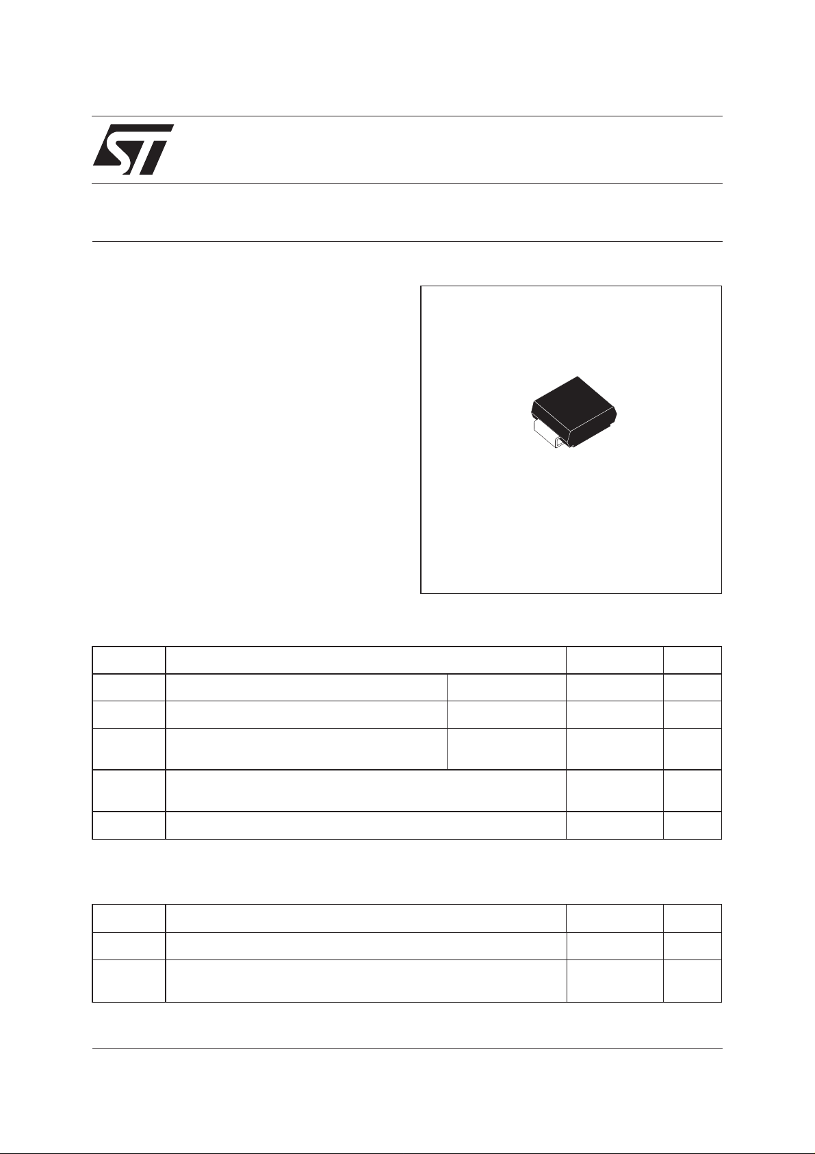
LOW VOLTAGE TRANSIL
SMB
(JEDEC DO-214AA)
TM
ABSOLUTE MAXIMUM RATINGS (T
amb
= 25°C)
Symbol Parameter Value Unit
P
PP
P
I
FSM
T
stg
T
j
T
L
Note 1 : For a surge greater than the maximum values, the diode will fail in short-circuit.
Peak pulse power dissipation (see note 1) Tj initial = T
Power dissipation on infinite heatsink T
amb
= 75°C
Non repetitive surge peak forward current tp=10ms
Tj initial = T
Storage temperature range
Maximum junction temperature
Maximum lead temperature for soldering during 10 s
amb
amb
600 W
5W
50 A
-65to+175
175
260 °C
THERMAL RESISTANCE
Symbol Parameter Value Unit
R
R
th (j-l)
th (j-a)
Junction to leads
Junction to ambient on printed circuit on recommended pad
20 °C/W
100 °C/W
layout
°C
°C
August 2001 - Ed : 2
1/4
Page 2
SMLVT3V3
ELECTRICAL CHARACTERISTICS (T
Symbol Parameter
V
V
V
I
I
αT
RM
BR
RM
PP
V
CL
F
Stand-off voltage.
Breakdown voltage.
Clamping voltage.
Leakage current @ VRM.
Peak pulse current.
Voltage temperature coefficient
Forward voltage drop
I
RM
@V
RM
VBR@I
max min max max max max
Type
AVVmAVAVA10
= 25°C)
amb
I
I
F
VV
CLVBR
R
VCL@I
PP
V
RM
VCL@I
I
I
PP
RM
PP
V
F
αTC
V
note 2 10/1000 µs 8/20 µs note 3 note 4
-4
/°C pF
SMLVT3V3 200 3.3 4.1 1 7.3 50 10.3 200 -5.3 5200
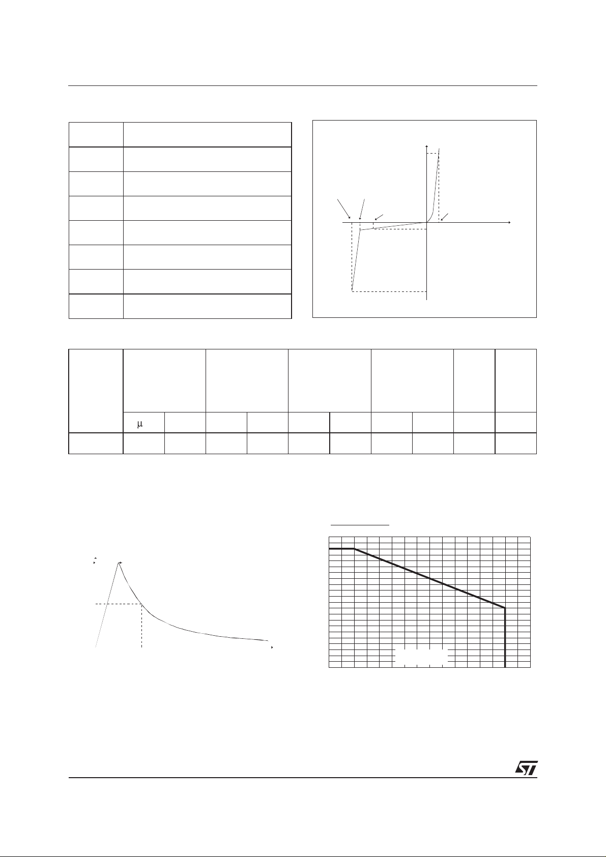
Fig. 1 : Peak pulse power dissipation versus initial
junction temperature (printed circuit board).
P [Tj initial]
PP
P [Tj initial = 25°C]PP
%I
PP
100
50
0
Note 2 : Pulse test : tp<50ms
Note 3 : ∆VBR= αT*(T
Note 4 : VR= 0V,F=1MHz.
10 µS
PLU SE WAVEFORM 10/1000 µS
1000 µS
amb
- 25)*VBR(25°C).
1.1
1.0
0.9
0.8
0.7
0.6
0.5
0.4
0.3
0.2
T
0.1
0.0
0 25 50 75 100 125 150 175 200
Tj initial (°C)
2/4
Page 3

SMLVT3V3
Fig. 2 : Peak pulse power versus exponential
pulse duration (Tj initial = 25°C).
Ppp(kW)
10.00
1.00
0.10
tp(ms)
0.01
0.01 0.10 1.00 10.00
Fig. 4 : Capacitance versus reverse applied
voltage (typical values).
C(PF)
5000
4000
3000
F=1MHZ
TJ=25°C
Fig. 3 : Clamping voltage versus peak pulse
current (Tj initial = 25°C).
Exponential waveform t
CL(V)
V
10
8
6
4
0.1 1.0 10.0 100.0
=20µs and tp= 1 ms.
p
TP=20 µS
TP=1MS
IPP(A)
Fig. 5 : Peak forward voltage drop versus peak
forward current (typical values).
2000
V
R(V )
1000
12345
Fig. 6 : Transient thermal impedance junction
ambient versus pulse duration.
Fig. 7 : Relative variation of leakage current
versus junction temperature.
Mounting on FR4 PC Board with Recommended
pad layout.
3/4
Page 4

SMLVT3V3
ORDER CODE
SM LVT 3V3
SURFACE MOUNT
PACKAGE MECHANICAL DATA
SMB (Plastic) - Jedec DO-214AA
E1
D
E
A1
c
A2
L
LOWVOLTAGETRANSIL
REF.
A1 1.90 2.15 2.45 0.075 0.085 0.096
A2 0.05 0.15 0.20 0.002 0.006 0.008
b 1.95 2.20 0.077 0.087
c 0.15 0.41 0.006 0.016
E 5.10 5.40 5.60 0.201 0.213 0.220
E1 4.05 4.30 4.60 0.159 0.169 0.181
D 3.30 3.60 3.95 0.130 0.142 0.156
b
L 0.75 1.15 1.60 0.030 0.045 0.063
STAND-OFF-VOLTAGE
DIMENSIONS
Millimeters Inches
Min. Typ. Max. Min. Typ. Max.
FOOTPRINT DIMENSIONS (Millimeter)
SMB Plastic.
Marking: Logo, data code, type code and cathod band
Weight = 0.12 g
2.3
Packaging : standard packaging is in tape and reel.
1.52 2.75
Informationfurnishedis believed tobeaccurate and reliable.However,STMicroelectronics assumes noresponsibilityfor the consequencesof
useofsuch information nor forany infringement of patentsorother rights ofthirdparties which may resultfrom its use. Nolicenseis granted by
implication or otherwise under any patent or patent rights of STMicroelectronics. Specifications mentioned in this publication are subject to
change without notice. This publication supersedes and replaces all information previously supplied.
STMicroelectronics products are not authorized for use as critical components in life support devices or systems without express written approval of STMicroelectronics.
Australia - Brazil - China - Finland - France - Germany - Hong Kong - India - Italy - Japan - Malaysia
Malta - Morocco - Singapore - Spain - Sweden - Switzerland - United Kingdom - U.S.A.
4/4
1.52
The ST logo is a registered trademark of STMicroelectronics
© 2001 STMicroelectronics - Printed in Italy - All rights reserved.
STMicroelectronics GROUP OF COMPANIES
http://www.st.com
 Loading...