


• HIGH GAIN LOW NOISE AMPLIFIERS
G
= 19 dB at 1.8 GHz
ms
• CURRENT EASY ADJUSTABLE BY AN
EXTERNAL RESIS TOR
• OPEN COLLECTOR OUTPUT
• TYPICAL SUPPLY VOLTAGE: 1.4-3.3 V
• TRANSITI ON FR E QU E N CY 4 2 GH z
• ULTRA MINIATURE SOT323-4L PACKAGE
(LEAD FREE)
APPLICATIONS
• WIDEBAND APPLICATIONS
• CELLULAR AND CORDLESS TELEPHONES
• HIGH FREQUENCY OSCILLATORS
DESCRIPTION
The SMA540B is a NPN Transistor integrating a current mirror as biasing. In this way the IC (collector
current) can be controlled setting the current at Bias
pin according to IC = 10 * IBIAS. The IBIAS current
is easy adjustable using an external resistor.
SMA540B is housed in ultra miniature SOT323-4L
package(LEAD FREE), the rel ative dimensions a re
1.15mmx1.8mm with 0.8mm thickness.
SMA540B
Active Biased RF Transistor
PRELIMINARY DATA
SOT323-4L (SC70)
ORDER CODE
SMA540BTR
Bias
Bias
Bias
Bias, 4
Bias, 4
Bias, 4
B, 1 E, 2
B, 1 E, 2
B, 1 E, 2
BRANDING
TBD
C, 3
C, 3
C, 3
ABSOLUTE MAXIMUM RATINGS
Symbol Parameter Value Unit
V
V
I
BIAS
P
T
T
T
ceo
ebo
I
c
I
b
tot
op
stg
j
Collector emitter voltage 4.5 V
Emitter base voltage 1.5 V
Collector current 40 mA
Base current 4 mA
BIAS Current 4 mA
Total dissipation, Ts = 107 oC
Operating temperature -40 to +85
Storage temperature -65 to +150
Max. operating junction temperature 150
120 mW
THERMAL RESISTANCE
R
thjs
January, 15 2003
Thermal Resistance Junction soldering point < 270
o
C/W
o
C
o
C
o
C
1/4

SMA540B
w
ELECTRICAL CHARACTERISTICS
(T
=25 oC,Z
A
Symbol Parameter Test Conditions Min. Typ. Max. Unit
(1)
Gms
2
|S21|
F
50Ω
P
-1dB
OIP3 Ouput third order intercept point Vd = 2V, Ic = 20mA
C
CB
CR Current Ratio (Ic/I
Note(1): Gms = | S21 / S12 |
PIN CONNECTION
= 50Ω, tested in circuit shown in fig.1, unless otherwise specified )
L/S
Maximum stable gain Vd = 2V, Ic = 20mA f = 1.8GHz 19 dB
Insertion power gain Vd = 2V, Ic = 20mA f = 1.8GHz 17.5 dB
Noise Figure
Output Power at 1dB
Compression Point
Vd = 2V, Ic = 5mA,
Zs = 50Ω
Vd = 2V, Ic = 20mA,
f = 1.8GHz 1.3 dB
f = 1.8GHz
f = 1.8GHz
9 dBm
19 dBm
Collector-base capacitance Vcb = 2V, f = 1MHz 0.13 pF
)I
Bias
= 0.5mA, Vd = 2V
Bias
10
4
12
SOT343
Typical co nf ig uration (Fig. 1)
SOT343
Bias
Bias
Bias
3
R
I
Bias, 4
Bias, 4
Bias, 4
Bias
Bias
Top vie
I
C
C, 3
C, 3
C, 3
Pin No. Description
1 BASE
2 EMITTER
3 COLLECTOR
4BIAS
V
D
I
D
RF Out
Bias-T
2/4
RF In
N.C.
Bias-T
B, 1 E, 2
B, 1 E, 2
B, 1 E, 2
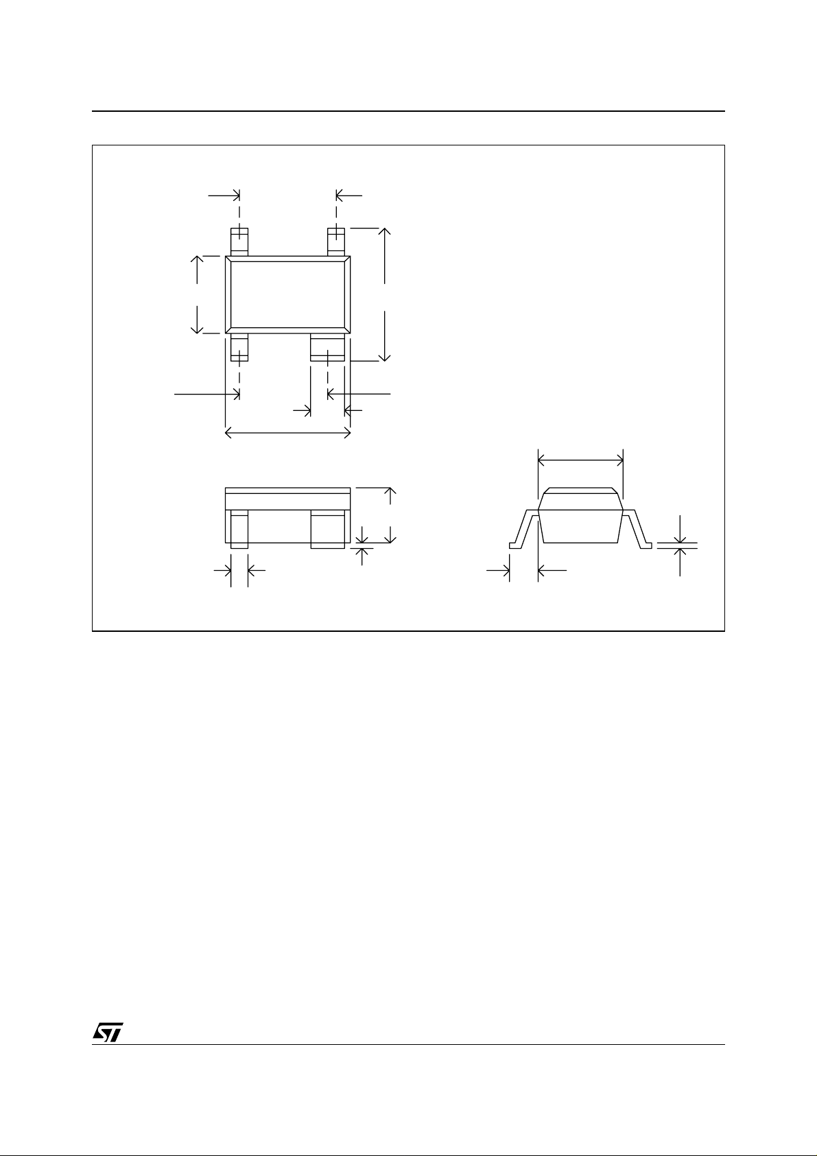
PACKAGE DIMENSIONS SOT323-4L (SC-70 4 leads)
1.30
SMA540B
1.15-1.35
2.00-2.20
1.90-2.10
0.80-1.00
0.25-0.35 0.00-0.10
1.15
0.55-0.65
1.15-1.35
0.45
0.10-0.20
3/4

SMA540B
p
Information furnished is believed to be ac curate and reli able. Howev er, STMicroel ectronics assumes no responsibilit y for the consequ ences
of use of such information nor for any infringement of patents or other rights of third parties which may result from its use. No license is granted
by implic ation or otherwise under any patent or patent rights of STMi croelectr onics. Specifications mentioned in thi s publicati on are sub j ect
to change without notice. This publication supersedes and replaces all information previously supplied. STMicroelectronics products are not
authorized for use as cri tical comp onents in life support dev i ces or systems wi t hout express written ap proval of STMi croelect roni cs .
The ST log o i s registered trademark of STMicro el ectronics
2003 STMicroelectroni cs - All Rig hts Reserved
All other names are the property of their respective owners.
Australi a - Brazil - Canada - China - Fi nland - France - Germa ny - Hong Kong - India - Israel - Italy - Jap an -
Malaysia - Malta - Morocco - Singapore - Spain - Sweden - Switzerland - United Kingdom - U.S.A.
STMicroelectron ics GROUP OF COMPANIES
htt
://www.st.com
4/4
 Loading...