

SGS Thomson Microelectronics SM4T33CA, SM4T36A, SM4T36CA, SM4T39A, SM4T39CA Datasheet
...
November 1992
SM4T6V8,A /220,A
SM4T6V8C, CA/220C,C A
TRANSI L
.PEAK PULS E POWER= 400 W @ 1ms.
.BREAKDOWN V OLT AGE RANGE :
From 6V8 to 220 V.
.UNI AND BIDIRECTIONAL TYPES.
.LOW CLAMPING FACTOR.
.FAST RESPONSE TIME:
T
clamping
: 1ps (0 V to VBR).
.JEDEC REGISTRED.
FEATURES
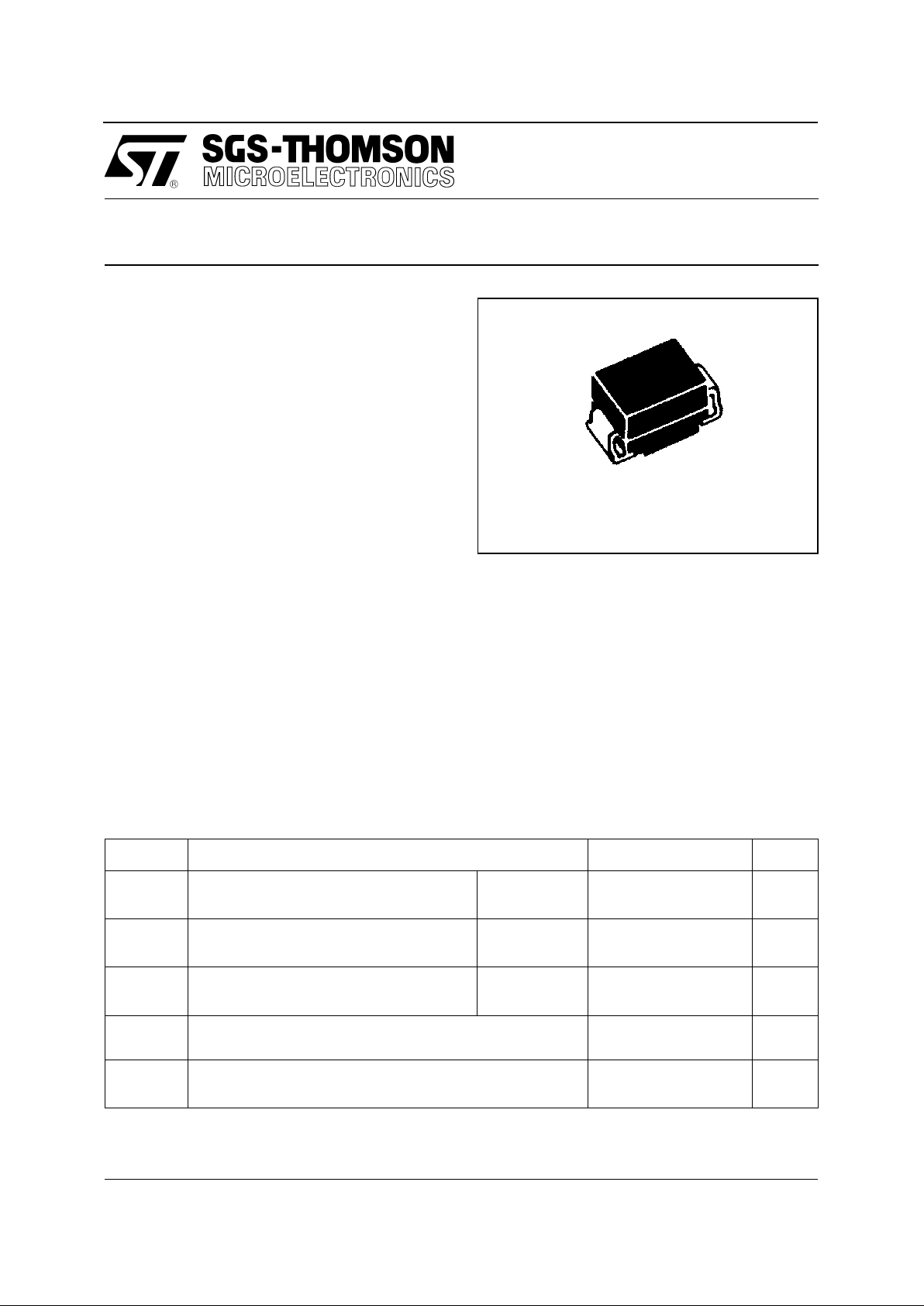
SOD 6
(Plastic)
Symbol Parameter Value Unit
P
p
Peak pulse power dissipation
See note 1 and derating curve Fig 1.
Tamb = 25°C 400 W
P Power dissipation on infinite heatsink
See note 1 and derating curve Fig 1.
Tlead = 50°C5 W
I
FSM
Non repetitive surge peak forward current.
For unidirectional types.
Tamb = 25°C
t =10 ms
50 A
T
stg
T
j
Storage and junction temperature range - 65 to + 175
150
°C
°C
T
L
Maximum lead temperature for soldering
during 10 s.
260 °C
ABSOLUTE RATINGS (limiting values)
DESCRIPTION
Transil diodes provide high overvoltage
protection by clamping action. Their
instantaneous reponse to transients makes them
praticularly suited to protect voltage sensitive
devices such as MOS Technology and low
voltage supplied IC’s.
MECHANICAL CHARACTERISTICS
.Body marked with : Logo, Date Code, Type
Code and Cathode Band (for unidirectional
types only).
.Full compatibility with both gluing and paste
soldering technologies.
.Excellent on board stability.
.Tinned copper leads.
.High temperature resistant resin.
1/7

ELECTRICAL CHARACTERISTICS
I
I
F
V
F
VV
CLVBR
V
RM
I
PP
I
RM
V
Symbol Parameter
V
RM
Stand-off voltage.
V
BR
Breakdown voltage.
V
CL
Clamping voltage.
I
RM
Leakage current @ VRM.
I
PP
Surge current.
αT
Voltage temperature coefficient.
V
F
Forward Voltage drop
VF < 3.5V @ IF = 25 A.
Symbol Parameter Value Unit
Rth (j-l) Junction-leads on infinite heatsink 20 °C/W
Rth (j-a) Junction to ambiant. on printed circuit.
With standard footprint dimensions.
100 °C/W
THERMAL RESISTANCES
TYPES
IRM @ V
RM
VBR @ IRVCL @ IPPVCL @ I
PP
αTC
max min nom max max max max typ
note2 10/1000µs8/20µs note3 note4
Uni
directional *Bidirectional *
µA VVVVmAVAVA10-4/°C(PF)
SM4T6V8
SM4T6V8A
SM4T7V5
SM4T7V5A
SM4T10
SM4T10A
SM4T12
SM4T12A
SM4T15
SM4T15A
SM4T18
SM4T18A
SM4T22
SM4T22A
SM4T24
SM4T24A
SM4T27
SM4T27A
SM4T30
SM4T30A
SM4T33
SM4T33A
SM4T36
SM4T36A
SM4T39
SM4T39
QD
QE
QF
QG
QN
QP
QS
QT
QW
QX
RD
RE
RH
RK
RL
RM
RN
RP
RQ
RR
RS
RT
RU
RV
RW
RX
SM4T6V8C
SM4T6V8CA
SM4T7V5C
SM4T7V5CA
SM4T10C
SM4T10CA
SM4T12C
SM4T12CA
SM4T15C
SM4T15CA
SM4T18C
SM4T18CA
SM4T22C
SM4T22CA
SM4T24C
SM4T24CA
SM4T27C
SM4T27CA
SM4T30C
SM4T30C4
SM4T33C
SM4T33CA
SM4T36C
SM4T36CA
SM4T39C
SM4T39
VD
VE
VF
VG
VN
VP
VS
VT
VW
VX
UD
UE
UH
UK
UL
UM
UN
UP
UQ
UR
US
UT
UU
UV
UW
UX
1000
1000
500
500
10
10
5
5
5
5
5
5
5
5
5
5
5
5
5
5
5
5
5
5
5
5
5.8
5.8
6.4
6.4
8.55
8.55
10.2
10.2
12.8
12.8
15.3
15.3
18.8
18.8
20.5
20.5
23.1
23.1
25.6
25.6
28.2
28.2
30.8
30.8
33.3
33.3
6.45
6.45
7.13
7.13
9.5
9.5
11.4
11.4
14.3
14.3
17.1
17.1
20.9
20.9
22.8
22.8
25.7
25.7
28.5
28.5
31.4
31.4
34.2
34.2
37.1
37.1
6.8
6.8
7.5
7.5
10
10
12
12
15
15
18
18
22
22
24
24
27
27
30
30
33
33
36
36
39
39
7.48
7.14
8.25
7.88
11
10.5
13.2
12.6
16.5
15.8
19.8
18.9
24.2
23.1
26.4
25.2
29.7
28.4
33
31.5
36.3
34.7
39.6
37.8
42.9
41.0
10
10
10
10
1
1
1
1
1
1
1
1
1
1
1
1
1
1
1
1
1
1
1
1
1
1
10.5
10.5
11.3
11.3
14.5
14.5
16.7
16.7
21.2
21.2
25.2
25.2
30.6
30.6
33.2
33.2
37.5
37.5
41.5
41.5
45.7
45.7
49.9
49.9
53.9
53.9
38
38
35.4
35.4
27.6
27.6
24
24
19
19
16
16
13
13
12
12
10.7
10.7
9.6
9.6
8.8
8.8
8
8
7.4
7.4
13.4
13.4
14.5
14.5
18.6
18.6
21.7
21.7
27.2
27.2
32.5
32.5
39.3
39.3
42.8
42.8
48.3
48.3
53.5
53.5
59.0
59.0
64.3
64.3
69.7
69.7
174
174
160
160
124
124
106
106
85
85
71
71
59
59
54
54
48
48
43
43
39
39
36
36
33
33
5.7
5.7
6.1
6.1
7.3
7.3
7.8
7.8
8.4
8.4
8.8
8.8
9.2
9.2
9.4
9.4
9.6
9.6
9.7
9.7
9.8
9.8
9.9
9.9
10.0
10.0
3500
3500
3100
3100
2000
2000
1550
1550
1200
1200
975
975
800
800
725
725
625
625
575
575
510
510
480
480
450
450
142
SM4Txx
2/7
143
Note 1 :
Note 2 :
Note 3 :
Note 4 :
For surges greater than the maximum values,
the diod e wi ll pr e sen t a sh ort - c ircu it An od e - Ca th od e.
Pulse test: TP < 50 ms.
∆VBR = αT * (Ta - 25) * V
BR(25°C)
.
VR = 0 V, F = 1 MHz. For bidirectional types,
capacit an c e va lue is divided by 2.
All parameters tested at 25 °C, except where indicated.
* = Marking
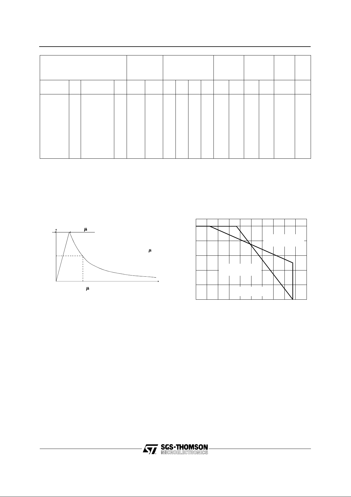
0
0%
20
40
60
80
100%
%
%
%
%
20
40 60 80 100 120 140 160 180 200
Tamb (˚c)
Peak Power
(on printed circuit).
Average Power
(on infinite heatsink).
Figure 1: Power dissipation derating versus
ambient temperature
10 s
1000 s
%I
PP
50
0
t
PULSE WAVEFORM 10/1000 s
100
TYPES IRM @ V
RM
VBR @ IRVCL @ IPPVCL @ I
PP
αTC
max min nom max max max max typ
note2 10/1000µs8/20µs note3 note4
Uni
directional *Bidirectional *
µA VVVVmAVAVA10-4/°C(PF)
SM4T68
SM4T68A
SM4T100
SM4T100A
SM4T150
SM4T150A
SM4T200
SM4T200A
SM4T220
SM4T220A
SN
SP
SW
SX
TH
TK
TS
TT
TU
TV
SM4T68C
SM4T68CA
SM4T100C
SM4T100CA
SM4T150C
SM4T150CA
SM4T200C
SM4T200CA
SM4T220C
SM4T220CA
WN
WP
WW
WX
XH
XK
XS
XT
XU
XV
5
5
5
5
5
5
5
5
5
5
58.1
58.1
85.5
85.5
128
128
171
171
188
188
64.6
64.6
95.0
95.0
143
143
190
190
209
209
68
68
100
100
150
150
200
200
220
220
74.8
71.4
110
105
165
158
220
210
242
231
1
1
1
1
1
1
1
1
1
1
92
92
137
137
207
207
274
274
328
328
4.3
4.3
2.9
2.9
2.0
2.0
1.5
1.5
1.4
1.4
121
121
178
178
265
265
353
353
388
388
19
19
13
13
9
9
6.5
6.5
6
6
10.4
10.4
10.6
10.6
10.8
10.8
10.8
10.8
10.8
10.8
270
270
200
200
145
145
120
120
110
110
SM4Txx
3/7
 Loading...