


MK5027
SS7 SIGNALLING
LINK CONTROLLER
August 1989
CMOS
FULLY COMPATIBLE WITH BOTH 8 OR 16
BITSYSTEMS
SYSTEM CLOCK RATE TO 10MHz. DATA
RATE UP TO 2.5Mbps FOR SS7 PROTOCOL
PROCESSING,7Mbps FOR TRANSPARENT
HDLCMODE
COMPLETELEVEL 2 IMPLEMENTATION
COMPATIBLE WITH 1988 CCITT, AT&T,
ANSI, AND BELLCORE SIGNALLING SYSTEMNUMBER 7 LINK LEVELPROTOCOLS
52 PIN PLCC AND 48-PIN DIP PIN-FOR-PIN
COMPATIBLE WITH THE SGS-THOMSON
X.25 CHIP (MK5025)AND NEARLY PIN-FORPIN COMPATIBLE WITH THE SGS-THOMSON VLANCE CHIP (MK5032)
BUFFER MANAGEMENTINCLUDES:
- InitializationBlock
- SeparateReceive and TransmitRings
- VariableDescriptor Ring and Window Sizes.
ON CHIP DMA CONTROL WITH PROGRAM-
MABLEBURST LENGTH
SELECTABLE BEC OR PCR RETRANSMIS-
SION METHODS, INCLUDING FORCED RETRANSMISSIONFOR PCR
HANDLESALL 7 SS7 TIMERS
HANDLESALL SS7 FRAME FORMATTING:
- Zerobit insertand delete
- FCSgeneration and detection
- Framedelimiting with flags
PROGRAMMABLE MINIMUM SIGNAL UNIT
SPACING(number of flags between SU’s)
HANDLES ALL SEQUENCING AND LINK
CONTROL
SELECTABLEFCS OF 16 OR 32 BITS.
TESTINGFACILITIES:
- InternalLoopback
- Silent Loopback
- OptionalInternal Data Clock Generation
- SelfTest
ALL INPUTS AND OUTPUTS ARE TTL COM-
PATIBLE
PROGRAMMABLE FOR FULL OR HALF DU-
PLEX OPERATION
DESCRIPTION
The SGS-THOMSON Signalling System #7 Signalling Link Controller (MK5027) is a VLSI semi-
conductor device which provides a complete link
control function conforming to the 1988 CCITT
version of SS7. This includes frame formatting,
transparency(so called ”bit-stufling”),error recovery by two types of retransmission, error monitoring, sequence number control, link status control, and FISU generation. One of the outstanding
features of the MK5027 is its buffer management
which includes on-chip DMA. Thisfeature allows
users to handlq multiple packets of receive and
transmit data at a time. (A conventional data linkcontrol chip plus a separate DMA chip wouldhandle data for only a single block at a time.) The
MK5027 maybe used with any of severalpopular
16 and 8 bit microprocessors, such as 68000,
6800, Z8000, Z80, LSI-11, 8086, 8088,8080, etc.
DIP48 PLCC52
VSS-GND
DAL07
DAL06
DAL05
DAL04
DAL03
DAL02
DAL01
DAL00
READ
INTR
DALI
DALO
DAS
BMO, BYTE, BUSREL
BMI, BUSAKO
HOLD, BUSRQ
ALE, AS
CS
ADR
READY
RESET
VSS-GND
24
HLDA
1
2
3
4
5
6
7
8
9
10
11
12
13
14
48
47
46
45
44
43
42
41
40
39
38
37
36
23
22
21
20
19
18
17
16
15
35
34
33
32
31
30
29
28
27
26
25
TCLK
A18
A19
A20
A21
A22
A23
RD
DSR, CTS
TD
SYSCLK
RCLK
DTR, RTS
VCC (+5V)
DAL08
DAL09
DAL10
DAL11
DAL12
DAL13
DAL14
DAL15
A16
A17
M
K
5
0
H
2
5
Figure 1: Pin Connection.
1/19
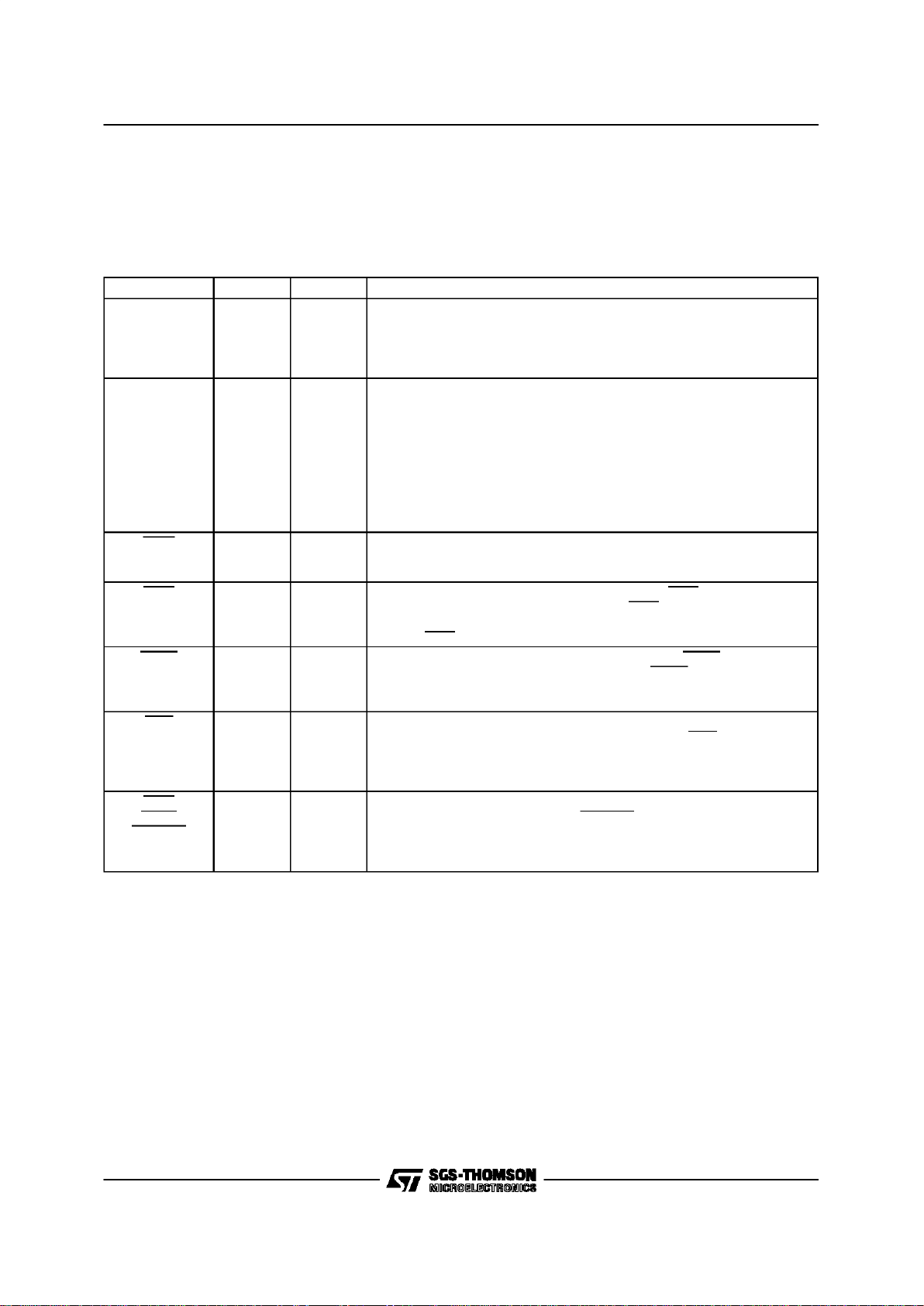
Table 1: PinDescription.
LEGEND:
I Input only O Output only
IO Input/Output 3S 3-State
OD Open Drain(no internal pull-up)
Signal Name Pin(s) Type Descriplion
DAL<15:00> 2-9
40-47
IO/3S The time multiplexedData Address bus.During the address portion of a
memory transfer, DALe15:00 contains the lower 16 bits ofthe memory
address.
Duringthe data portion of a memory transfer, DAL<15:00> contains the
read or write data, depending on thetype of transfer.
READ 10 IO/3S READ indicates the type of operationthat the bus controlleris performing
during a bus transaction. READ is driven by the MK5027 only while it is
the BUS MASTER. READ isvalid during the entire bus transactionand is
tristatedat all othertimes.
MK5027 as a Bus Slave:
READ = HIGH - Data is placed on the DAL lines by the chip.
READ = LOW- Data is taken off theDAL lines by the chip.
MK5027 as a Bus Master:
READ = HIGH- Data is taken off the DAL lines by the chip.
READ = LOW - Data is placed on the DAL lines by the chip.
INTR 11 O/OD INTERRUPT is an attention interruptline that indicates that one or moreof
the following CSR0 status flags isset: MISS, MERR,RINT, TINT or PINT.
INTERRUPT is enabled by CSR0<0.9>, INEA = 1.
DALI 12 O/3S DAL IN is an external bus transceiver control line. DALIis driven by the
MK5027 only whileit is the BUS MASTER. DALIis assertedby the
MK5027 when | ads from the DAL lines during the data portion of a READ
transfer. DALIis not asserted during a WRITE transfer.
DALO 13 O/3S DAL OUT isan external bus transceiver control line. DALOis driven by
the MK5027 onlywhile it is the BUS MASTER. DALOis asserted by the
MK5027 when itdrives the DAL linesduring theaddress portion of a
READ transfer orfor the duration of a WRITE transfer.
DAS 14 IO/3S DATA STROBE defines the dataportio,n ofa transaction. By definition,
data is stable and valid at the low to hightransition of DAS.This signal is
drivenby the MK5027 while it is the BUS MASTER.During the BUS
SLAVE operation, this pin is used as an input.At all other times the signal
is tristated.
BMO
BYTE
BUSREL
15 IO/3S I/O pins 15and 16 are programmable through CSR4. If bit 06 of CSR4 is
set to a one, pin 15 becomes inputBUSRELand is used by the hostto
signalthe MK5027 toterminate a DMA burst after thecurrent bus transfer
has completed. If bit 06 is clear the pin 15 is an output and behaves as
described below for pin16.
Note: Pin out shown is for 48 pin dip.
MK5027
2/19

Table 1: PinDescription (continued)
Signal Name Pin(s) Type Descriplion
BM1
BUSAKO
16 O/3S Pins 15 and 16 are programmable though bit 00 ofCSR4 (BCON).
If CSR4<00> BCON = 0,
I/O PIN 15 = BMO (O/3S)
I/O PIN 16 = BM1 (O/3S)
BYTE MASK<1:0> indicates the byte(s) on the DAL to be read or written
during this bus transaction. MK5027 drives these lines only as a Bus
Master. MK5027 ignores the BM lines whenit is a Bus Slave.
Byte selection is done as outlined inthe following table.
BM1 BM0 TYPE OF TRANSFER
LOW LOW ENTIRE WORD
LOW HIGH UPPER BYTE (DAL<15:08>)
HIGH LOW LOWER BYTE(DAL<07:00>)
HIGH HIGH NONE
If CSR4<00>BCON = 1,
I/O PIN 15 = BYTE (O/3S)
I/O PIN 16 = BUSAKO(O)
Byte selection is done using the BYTE line and DAL<00> latched during
the address portion of the bus transaction. MK5027drives BYTE only a
Bus Master and ignores it whena Bus Slave. Byte selectionis done as
outlined in the followingtable.
BYTE DAL<00> TYPE OF TRANSFER
LOW LOW ENTIRE WORD
LOW HIGH ILLEGAL CONDITION
HIGH LOW LOWER BYTE
HIGH HIGH UPPER BYTE
BUSAKOis a bus request daisy chain output. If MK5027 is notrequesting
the bus andit receives HLDA, BUSAKOwill bedriven low. If MK5027 is
requesting the bus when it receives HLDA, BUSAKOwill remain high.
Note: All transfers are entire word unlessthe MK5027 is configuredfor 8
bit operation.
HOLD
BUSRQ
17 IO/OD Pins 17is configuredthrough bit 0of CSR4.
If CSR4<00> BCON = 0,
I/O PIN 17 = HOLD
HOLD request is asserted by MK5027 when it requires a DMA cycle, if
HLDA is inactive, regardless of the previous state of the HOLD pin.
HOLD is heldlow for the entire ensuing bus transaction.
If CSR4<00> BCON = 1,
I/O PIN 17 = BUSRQ
BUSRQ is asserted by MK5027 when it requires a DMA cycleif the prior
state of theBUSRQpin was high and HLDA is inactive. BUSRQis held
low for the entire ensuing bus transaction.
ALE
AS
18 O/3S The active level of ADDRESS STROBE is programmable throughCSR4.
The address portion of a bustransfer occurs while this signal is at its
asserted level. This signal is driven by MK5027 while itis the BUS
MASTER. At all other times, the signal is tristated.
If CSR4<01> ACON = 0,
I/O PIN 18 = ALE
ADDRESSLATCHENABLE isused to demultiplex the DALlines and define
theaddress portion of thetransferand remains low during the data portion.
If CSR4<01> ACON = 1,
I/O PIN 18 = AS
As AS,the signalpulses lowduring the address portion of the bus
transfer. The low to hightransition of AScan be used by a slavedevice to
strobe the address into a register.
AS is effectively the inversion of ALE.
HLDA 19 I HOLD AKNOWLEDGE is theresponse to HOLD. Whe nHLDAis low inresponse
to MK5027’s assertion of HOLD, theMK5027 isthe BusMaster . HLDA should be
desasse rted ONLY a fter HOLDhas been re leased by the MK 5027.
MK5027
3/19

Table 1: PinDescription (continued)
Signal Name Pin(s) Type Descriplion
CS 20 I CHIP SELECT indicates, when low, that the MK5027 is the slave device
for the data transfer.CS must be valid througoutthe enture transaction.
ADR 21 I ADDRESS selects the Register Address Port or the Register Data Port. It
must be validthroughout thedata portion of thetransfer and is onlyused
by the chipwhen CS is low.
ADR PORT
LOW REGISTER DATA PORT
HIGH REGISTER ADDRESS PORT
READY 22 IO/OD When the MK5027 is a Bus Master, READYis an asynchronous
acknowledgement from the bus memory that memory will accept data in a
WRITE cycle or that memory has put data on the DAL lines in a READ
cycle.
As a bus Slave, the MK5027 asserts READYwhen it hasput data on the
DAL lines during a READcycle oris about to take datafrom the DAL lines
during WRITE cycle.READY is a response to DAS and it will be released
after DASor CS is negated.
RESET 23 I RESET isthe Bus signal that will cause MK5027 to cease operation, clear
its internal logic and enter an idle state with the Power Off bit of CSR0 set.
TCLK 25 I TRANSMIT CLOCK. A 1xclock input for transmitter timing. TD changes
on the falling edge of TCLK. The frequency of TCLKmay not be greater
than the frequency of SYSCLK.
DTR
RTS
26 IO DATA TERMINAL READY, REQUEST TO SEND. Modem controlpin. Pin
26 is configurablethrough CSR5. This pin can be programmed to behave
as output RTS or as programmable IO pin DTR. If configured as RTS, the
MK5027 will assert this pin if it has data to send and throughout the
transmission of a signal unit.
RCLK 27 I RECEIVE CLOCK. A 1x clock input for receiver timing. RD is sampled on
the rising edge of RCLK. The frequency of RCLK may not be greater than
the frequency of SYSCLK.
SYSCLK 28 I SYSTEM CLOCK. System clock used for internaltiming of the MK5027.
SYSCLK should be a square wave, of frequency up to 10MHz.
TD 29 O TRANSMIT DATA. Transmit serial dataoutput.
DSR
CTS
30 IO DATA SET READY, CLEAR TOSEND. Modem Control Pin. Pin 30 is
configurablethrough CSR5. This pin can beprogrammed to behave as
input CTS or as programmable IO pin DSR. If configured asCTS, the
MK5027 will transmit allones while CTS is high.
RD 31 I RECEIVE DATA. Received serialdata input.
A<23:16> 32-39 O/3S Address bits <23:16> used in conjunctionwith DAL <15:00> to produce a
24 bit address. MK5027 drives these lines only as a Bus Master.
A23-A20may be driven continuouslyas described in the CSR4<7>BAEN
bit.
VSS-GND 1, 24 GroundPins
VCC 48 Power Supply Pin
+5.0 VDC ± 5%
MK5027
4/19
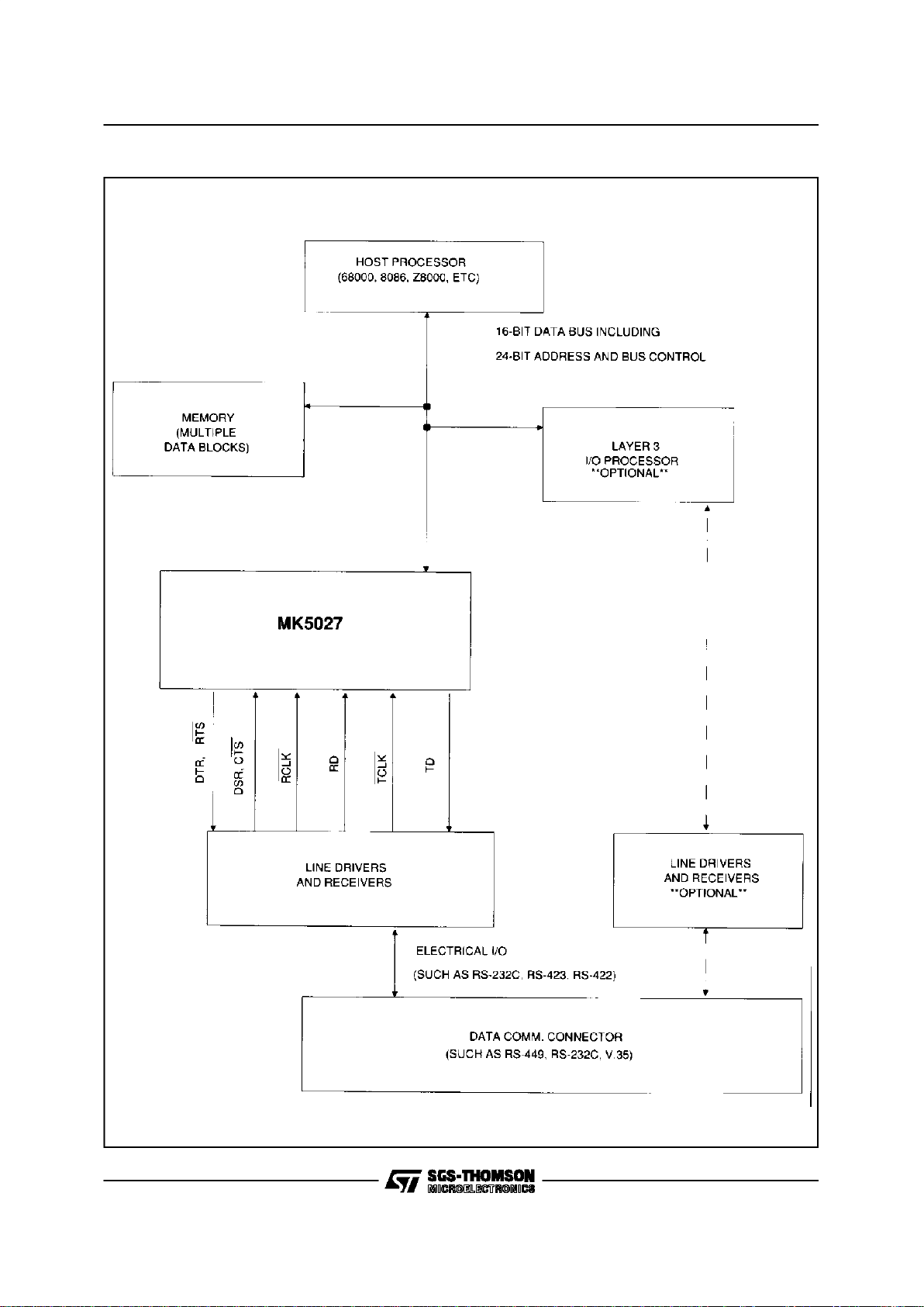
Figure2: PossibleSystem Configurationfor the MK5027.
MK5027
5/19
OPERATIONALDECRIPTION
The SGS-THOMSON Signalling System #7 Signalling Link Controller (MK5027) device is a VLSI
product intended for data communicationapplicationsrequiring SS7link level control. The MK5027
will perform all frame formatting, such as: frame
delimiting with flags, FCS generation and detection. It will also perform all error recovery and link
control. The MK5027 also includes a buffer management mechanism that allow the user to transmit and/or receive multiple MSU’s. Contained in
the buffer management is an on-chip dual chan-
nel DMA: one channel for receive and one channel for transmit. The MK5027handles error recovery andlink statussignalling.
The MK5027 is intended to be used with any
popular 16 or 8 bit microprocessor. Possible system configurationfor the MK5027 is shown in Figure 2. The MK5027 will move multiple blocks of
receive and transmit data directly into and out of
memory through the host’s bus. An I/O acceleration processor in Figure 2 is recommended, but
not required.
DALI
DALO
HLDA
HOLD
ALE, AS
BM0
BM1
DAS
READ
INTR
ADR
READY
DTR, RTS
DSR, CTS
CS
FIRMWARE
ROM
MICRO
CONTROLLER
TIMERS
DMA
CONTROLLER
CONTROL / STATUS
REGISTERS 0 - 5
SYSCLK
INTERNAL BUS
RECEIVER
FIFO
TRANSMITTER
FIFO
RECEIVER TRANSMITTER
LOOPBACK
TEST
RD
RCLK
TCLK
TD
VSS - GND
RESET
VCC
DAL<15:00>
A <23:16>
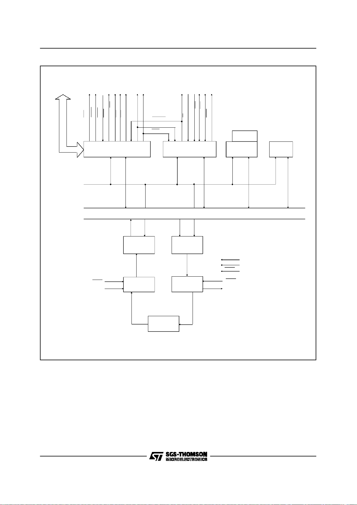
Figure3: MK5027 SimplifiedBlockDiagram.
MK5027
6/19

All signal pins on the MK5027 are TTL compatible. This has the advantage of making the
MK5027 in- dependent of the physical interface.
As shown in Figure 2. Iine drivers and receivers
are used for electrical- connectionto the physical
layer.
SERIALINTERFACE
The MK5027 provides two separate serial channels: one for received data and one for transmitted data. These serial channels are completely
separate and may be run at different clock frequenciesThe receiver is responsible for recognizing frame boundries. removal of inserted zeroes
(for transparency) and checking the incoming
FCS. Signal units with in correct FCS values are
discarded. The receiver also parallelizes the incoming data which is placed into the receive data
buffers within the receive descriptor ring The
transmitteris responsiblefor framing and serializing the data frames placed in the transmit descriptor ring. The transmitter calculates the FCS
of the outgoing data and appends it to the data
The transmitter generates flag sequences for inter-signal unit fill, at least two flags are transmitted between adjacent signal units. The FCS calculations for both directions of serial data
optionally follow either the 16 bit CRC CCITT or
the 32-bit CRC32 algorithmsFCS generationand
checkingcan also be optionallydisabled if necessary.
MICROPROCESSOR INTERFACE
The MK5027 contains a dual channel DMA on
chip to handle data transfers to and from the host
mem-ory. Allaccess to the initializationblock and
descriptor rings is handled in this way The address bus is 24 bits wide and does not use any
segmentation or paging methods. Data transfers
can optionally be 8 and 16 bit operations. this allows easy interfacingwith both 8 and 16 bit processors DMA transfers can be up to 1. 8 or an unlimited number of words per transfer under
program control During bus slave operation the
MK5027 allows access to its 6 control/status registers which are used to monitor and control the
chip. These registers are used to control link procedures, configure interface options, control and
monitor interrupt status. and more. Bus slave
mode also allows both 8 and 16 bit accesses.
BUFFERMANAGEMENT
The basic organization of the buffer management
is a circular queue of tasks in memory called descriptor rings. There are separate rings to describe the transmit and receive operations. Up to
128 buffers may be queued-up on a descriptor
ring awaiting execution by the MK5027 The descriptor ring has a segment assigned to each
buffer. Each segmentholds a pointer for the starting address of the buffer. and holds a value for
the lengthof the bufferin bytes.
Each segment also contains two control bits
called OWNA and OWNB, which denote whether
the MK5027. the HOST. or the l/O ACCELERATION PROCESSOR (if present) ”owns” the buffer. For transmit. when the MK5027owns the buffer. the MK5027 is allowed and commanded to
transmit the buffer When the MK5027 does not
own the buffer, it will not transmit that buffer. For
receive. when the MK5027 owns a buffer. it may
place received data into that buffer. Conversely.
when the MK5027 does not own a receive buffer, it will not place received data in that buffer.
The MK5027 buffer managementmechanism will
handly signal units which are longer than the
length of an individual buffer. This is done by a
chaining method which utilizes multiple buffers.
The MK5027 tests the next segment in the descriptor ring in a ”look ahead” manner. If the
packet is too long for one buffer, the next bufferwill be used after filling the first buffer: that is,
”chained”. The MK5027 will then ”look ahead” to
the next buffer, and chain that buffer if necessary,
and so on The operational parameters for the
buffer management are defined by the user
in the initialization block The parameters defined
include the basic mode of operation. the number
of entries for the transmitter and receiver descriptor rings.etc.
MK5027
7/19

RECEIVERDESCRIPTOR RINGS
DESCRIPTOR 0
BUFFERSTATUS
BUFFERADDRESS
BUFFER SIZE
BUFFER MSGCOUNT
DESCRIPTOR 1
DESCRIPTOR M
TRANSMITDESCRIPTOR RINGS
DESCRIPTOR 0
BUFFER STATUS
BUFFER ADDRESS
BUFFER SIZE
BUFFER MSG COUNT
DESCRIPTOR 1
DESCRIPTOR N
BUFFER
N
BUFFER
1
BUFFER
0
TRANSMIT BUFFER
BUFFER
M
BUFFER
1
BUFFER
0
RECEIVE BUFFER
CSR 2, CSR3
POINTER TO
INITIALIZATI ON BLOCK
INITIALIZATI ON BLOCK
MODE
TIMER VALUES
RX DESCRIPTOR
TX DESCRIPTOR
POINTER
POINTER
FRAME ADDRESS
FIELDS
STATUS
BUFFER ADDRESS
STATUS BUFFER
ERROR COUNTERS
XID/TEST TRANSMIT
DESCRIPTOR POINTER
XID/TEST RECEIVE
DESCRIPTORPOINTER
RECEIVE BUFFER
TRANSMIT BUFFER
XID/TEST
XID/TEST
Figure4: MK5027 Buffer Management.
MK5027
8/19

SIGNALLING UNIT REPERTOIRE
Thesignal unitrepertoire of theMK5027 is shown
in Table 1. This set conforms to the 1988 CCITT
specificationfor level2 of SignallingSystem #7.
The definitions for the symbols for the frame
types are:
Name Definition
F
FSN
BSN
FIB
BIB
LI
X
SIO
SIF
SF
FCS
Flag Sequence
Forward Sequence Number
Backward Sequences Number
Forward Indicator Bit
Backward Indicator Bit
Lenght Indicator
Programmed As Zeroes
Signalling Information Octet
Service Information Field
Satus Field
Frame Check Sequence
Table 1: MK5027Signal Unit Repertoire.
MK5027
9/19

MK5027ELECTRICAL SPECIFICATIONS
ABSOLUTE MAXIMUM RATINGS
Temperature under Bias –25°Cto +100°C
Storage Temperature –65°Cto +150°C
Voltage on AnyPin with Respect to Ground –0.5V to VCC +0.5V
Power Dissipation 0.50W
Stresses above those listed under ”Absolute Maximum Ratings” may cause permanent damage to the above device. This isa stress rating only
and functional operation of the device atthese or any other condition above those indicated in the operationalsections of this specification is
not implied. Exposure to absolutemaximum rating conditions for extended periods may affectdevice reliability.
DC CHARACTERISTICS
T
A
=0 °Cto70°C, VCC= +5V±5 percentunlessotherwise specified.
Symbol Parameter Min. Typ. Max. Units
V
IL
-0.5 +0.8 V
V
IH
+2.0 VCC+0.5 V
V
OL
@ IOL = 3.2 mA +0.5 V
V
OH
@ IOH= -0.4 mA +2.4 V
I
IL
@ VIN = 0.4 to V
CC
+10 mA
I
CC
@ TSCT = 100 ns 50 µA
CAPACITANCE
f = 1MHz
Symbol Parameter Min. Typ. Max. Units
C
IN
Capacitance on Input pins 10 pF
C
OUT
Capacitance on Output Pins 10 pF
C
IO
Capacitance on I/O pins 20 pF
AC TIMING SPECIFICATIONS
T
A
=0°Cto70°C, VCC= +5V ±5 percent,unless otherwisespecified.
No Signal Symbol Parameter
Test
Condition
Min. Typ. Max. Units
1 SYSCLK T
SCT
SYSCLK period 100 20000 ns
2 SYSCLK T
SCL
SYSCLK low time 45 ns
3 SYSCLK T
SCH
SYSCLK hightime 45 ns
4 SYSCLK T
SCR
Rise time of SYSCLK 0 8 ns
5 SYSCLK T
SCF
Fall time of SYSCLK 0 8 ns
6 TCLK T
TCT
TCLKperiod 140 ns
7 TCLK T
TCL
TCLK low time 63 ns
8 TCLK T
TCH
TCLKhigh time 63 ns
9 TCLK T
TCR
Rise time of TCLK CL = 50 pF 0 8 ns
10 TCLK T
TCF
Fall time of TCLK 0 8 ns
11 TD T
TDP
TD datapropagation delay after the
falling edge of TCLK
CL = 50 pF 40 ns
12 TD T
TDH
TD datahold time after the falling edge
of TCLK
5ns
MK5027
10/19

AC TIMING SPECIFICATIONS (Continued)
T
A
=0°Cto70°C, VCC= +5V ±5 percent,unless otherwisespecified.
No Signal Symbol Parameter
Test
Conditions
Min. Typ. Max. Units
13 RCLK T
RCT
RCLK period 140 ns
14 RCLK T
RCH
RCLK high time 63 ns
15 RCLK T
RCL
RCLK low time 63 ns
16 RCLK T
RCR
Rise time of RCLK 0 8 ns
17 RCLK T
RCF
Fall time of RCLK 0 8 ns
18 RD T
RDR
RD datarise time 0 8 ns
19 RD T
RDF
RD datafall time 0 8 ns
20 RD T
RDH
RD holdtime after rising edge of
RCLK
5ns
21 RD T
RDS
RD setuptime prior to rising edge of
RCLK
30 ns
22 A/DAL T
DOFF
Bus Master driver disable after rising
edge of HOLD
050ns
23 A/DAL T
DON
Bus Master driver enable after falling
edge of HLDA
TSCT =100ns 0 200 ns
24 HLDA T
HHA
Delay to fallingedge of HLDAfrom
falling edge of HOLD (Bus Master)
0ns
25 RESET T
RW
RESET pulse width 30 ns
26 A/DAL T
CYCLE
Read/write, address/data Cycle Time TSCT =100ns 600 ns
27 A T
XAS
Address setup time to falling edge
of ALE
100 ns
28 A T
XAH
Address hold time after the rising
edge of DAS
50 ns
29 DAL T
AS
Address setup time to falling edge
of ALE
75 ns
30 DAL T
AH
Address hold time after the falling
edge ofALE
20 ns
31 DAL T
RDAS
Data setup time to thefalling edge
of DAS(Bus Master read)
55 ns
32 DAL T
RDAH
Data holdtime afterthe risingedge
of DAS(bus master read)
0ns
33 DAL T
DDAS
Data setup time to the falling edgeof
DAS (bus master write)
0ns
34 DAL T
WDS
Data setup time to the rising edgeof
DAS (bus master write)
250 ns
35 DAL T
WDH
Data holdtime tothe rising edge of
DAS (bus slave write)
35 ns
36 DAL T
SRDH
Data holdtime afterthe risingedge
of DAS (bus slave read)
TSCT =100ns 0 35 ns
37 DAL T
SWDH
Data holdtime afterthe risingedge
of DAS (bus slave write)
0ns
38 DAL T
SWDS
Data setup time to the falling edgeof
DAS (bus slave write)
0ns
39 ALE T
ALEW
ALE width high 110 ns
40 ALE T
DSW
Delay from rising edge od DASto
the rising edge of ALE
70 ns
41 DAS T
DSW
DAS width low 200 ns
MK5027
11/19

AC TIMING SPECIFICATIONS (Continued)
T
A
=0°Cto70°C, VCC= +5V ±5 percent,unless otherwisespecified.
No Signal Symbol Parameter
Test
Conditions
Min. Typ. Max. Units
42 DAS T
ADAS
Delay from the falling edge ofALE to
the falling edge of DAS
80 ns
43 DAS T
RIDF
Delay from the rising edge of DALO
to the fallingedge of DAS(bus
master read)
35 ns
44 DAS T
RDYS
Delay from the falling edge of
READYto the fallingedge of DAS
T
ARYD
= 300ns
T
SCT
= 100ns
120 200 ns
45 DALI T
ROIF
Delay from the rising edge of DALO
to the fallingedge of DALI(bus
master read)
70 ns
46 DALI T
RIS
DALIsetup time to the rising edge of
DAS (bus master read)
150 ns
47 DALI T
RIH
DALIhold time afterthe risingedge
of DAS(bus master read)
0ns
48 DALI T
RIOF
Delay from the rising edge of DALI
to the fallingedge of DALO(bus
master read)
70 ns
49 DALO T
OS
DALOsetup time to the falling edge
of ALE (bus master read)
110 ns
50 DALO T
ROH
DALOhold time afterthe falling
edge ofALE (busmasterread)
35 ns
51 DALO T
WDSI
Delay from the rising edge of DAS to
the rising edge of DALO(bus master
write)
50 ns
52 CS T
CSH
CS hold time after the risingedge of
DAS (bus slave)
0ns
53 CS T
CSS
CS setup time to the fallingedge of
DAS (bus slave)
0ns
54 ADR T
SAH
ADR hold time after the rising edge
of DAS (bus slave)
0ns
55 ADR T
SAS
ADR setup time to the falling edge of
DAS (bus slave)
0ns
56 READY T
ARYD
Delay from the falling edge ofALE to
the falling edge of READYto Insure
a Minimum Bus Cycle Time (600ns)
T
SCT
= 100ns 150 ns
57 READY T
SRDS
Data setup time to the falling edgeof
READY(bus slave read)
75 ns
58 READY T
RDYH
READYhold time after the rising
edge of DAS (bus master)
0ns
59 READY T
SRYH
READYhold time after the rising
edge of DAS (bus slave)
T
SCT
= 100ns 0 35 ns
60 READY T
RSH
READ holdtime afterrhe rising edge
of DAS(bus slave)
0ns
61 READ T
SRS
READ setup time after rhe rising
edge of DAS (bus slave)
0ns
62 READY T
RDYD
Delay from falling edge of DASto
falling edge of READY(bus slave)
T
SCT
= 100ns 200 ns
MK5027
12/19

C
L
0.4 mA
CR
CR
CR
CR
1
2
3
4
R1 = 1.2K
CR1 - CR4 = 1N914 or EQUIV
TEST
POINT
FROM
OUTPUT
UNDER
TEST
R1 = 1.4K
C
L
VccVcc
C =50pF min @ 1 MHz
L
FROM
OUTPUT
UNDER
TEST
NOTE: This load is used on all outputs except INTR, HOLD, READY.
NOTE: This load is used on open
drain outputs INTR, HOLD,READY.
RCLK
13
15
14
16 17
21
20
19
18
RD
12
6
87
10
11
9
TD
TCLK
”0”
O.8 V
O.8 V
90 %
”1”
2.0 V
2.0 V
10 %
OUTPUT
INPUT
FLOAT
TIMING MEASUREMENTS ARE MADE AT THE FOLLOWING VOLTAGES,
UNLESS OTHERWISE SPECIFIED:
Figure 6: MK5027Serial Link Timing Diagram
Figure5A: TTL Output Load Diagram. Figure5B: Open Drain OutputLoad Diagram.
MK5027
13/19

Figure7: MK5027 Bus Master Timing Diagram (read).
Note: The BusMaster cycle time willincrease from a minimum of 600ns in 100ns steps until the slave device return READY.
MK5027
14/19

Figure8: MK5027 Bus Master Timing Diagram (write).
Note: The BusMaster cycle time willincrease from a minimum of 600ns in 100ns steps until the slave device return READY.
MK5027
15/19

Figure9: MK5027 Bus Slave Timing Diagram (read)
Figure10: MK5027Bus Slave Timing Diagram (write)
MK5027
16/19

DIP48PACKAGE MECHANICAL DATA
DIM.
mm inch
MIN. TYP. MAX. MIN. TYP. MAX.
a1 0.63 0.025
b 0.45 0.018
b1 0.23 0.31 0.009 0.012
b2 1.27 0.050
D 62.74 2.470
E 15.2 16.68 0.598 0.657
e 2.54 0.100
e3 58.42 2.300
F 14.1 0.555
I 4.445 0.175
L 3.3 0.130
MK5027
17/19

PLCC52PACKAGE MECHANICAL DATA
DIM.
mm inch
MIN. TYP. MAX. MIN. TYP. MAX.
A 4.20 5.08 0.165 0.20
A1 0.51 0.020
A3 2.29 3.30 0.090 0.13
B 0.33 0.53 0.013 0.021
B1 0.66 0.81 0.026 0.032
C 0.25 0.01
D 19.94 20.19 0.785 0.795
D1 19.05 19.20 0.750 0.756
D2 17.53 18.54 0.690 0.730
D3 15.24 0.60
E 19.94 20.19 0.785 0.795
E1 19.05 19.20 0.750 0.756
E2 17.53 18.54 0.690 0.730
E3 15.24 0.60
e 1.27 0.05
L 0.64 0.025
L1 1.53 0.060
M 1.07 1.22 0.042 0.048
M1 1.07 1.42 0.042 0.056
MK5027
18/19

Information furnished is believed to be accurate and reliable. However,SGS-THOMSON Microelectronics assumes no responsibility for the
consequences of use ofsuch information nor for any infringement of patents or other rights of third parties which may result from its use. No
license is granted by implication or otherwiseunder any patent or patent rightsof SGS-THOMSONMicroelectronics. Specification mentioned
in this publication are subject to change without notice. This publication supersedes and replaces all information previously supplied.
SGS-THOMSON Microelectronics products arenotauthorizedfor use as critical components in life support devices orsystems without express
written approval of SGS-THOMSON Microelectronics.
1996 SGS-THOMSON Microelectronics – Printed in Italy– All RightsReserved
SGS-THOMSON Microelectronics GROUP OFCOMPANIES
Australia - Brazil - Canada- China - France - Germany - Hong Kong - Italy - Japan - Korea- Malaysia - Malta - Morocco - The Netherlands -
Singapore- Spain- Sweden - Switzerland - Taiwan - Thailand - United Kingdom - U.S.A.
MK5027
19/19
 Loading...