

Page 1
PRELIMINARY INFORMATION
Dual 1 to 8 Buffalo™ Clock Driver
MK74CB217
Description
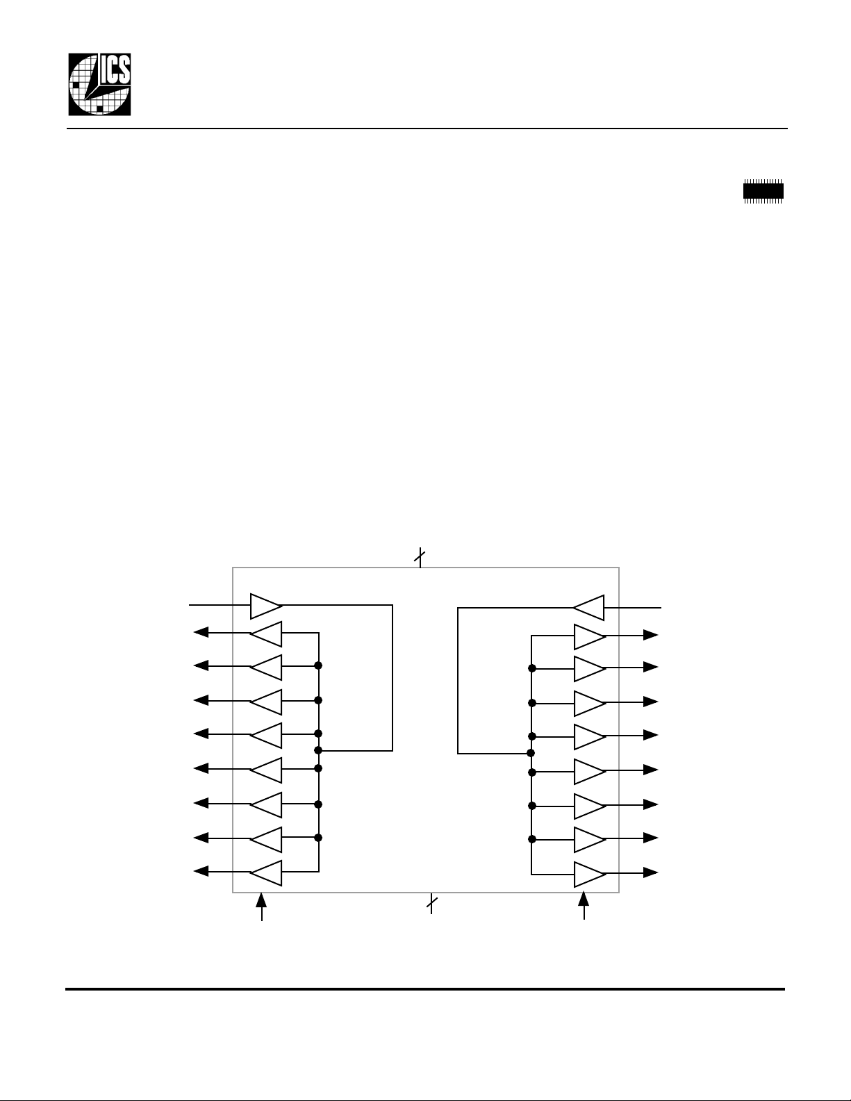
The MK74CB217 Buffalo™ is a monolithic
CMOS high speed clock driver. It consists of two
identical single input to eight low-skew output,
non-inverting clock drivers. This eliminates
concerns of part to part matching in many
systems. The MK74CB217 is packaged in the
tiny 28 pin SSOP, which uses the same board
space as the narrow 16 pin SOIC. The inputs can
be connected together for a 1 to 16 fanout buffer.
A quad 1 to 4, and PECL versions, are also
available. Consult us for more details.
Block Diagram
Features
• Tiny 28 pin SSOP (150 mil) package
• Dual one input to eight output clock drivers
• Outputs are skew matched to within 250 ps
• A outputs and B outputs matched to 250 ps
• 3.3 V or 5 V supply voltage
• Output Enable tri-states each bank of eight
• Clock speeds up to 200 MHz
Family of ICS Parts
The MK74CB217 Buffalo™ is designed to be used
with ICS’s clock synthesizer devices. The inputs of the
Buffalo are matched to the outputs of ICS clock
synthesizers. Consult ICS for applications support.
VDD
4
INA
QA0
QA1
QA2
QA3
QA4
QA5
QA6
QA7
4
OEA (all A outputs)
GND
MDS74CB217A 1 Revision 12299 Printed 2/22/00
IntegratedCircuit Systems, Inc. • 525 Race Street • San Jose •CA •95126•(408) 295-9800tel • www.icst.com
OEB (all B outputs)
INB
QB0
QB1
QB2
QB3
QB4
QB5
QB6
QB7
Page 2
PRELIMINARY INFORMATION
Dual 1 to 8 Buffalo™ Clock Driver
MK74CB217
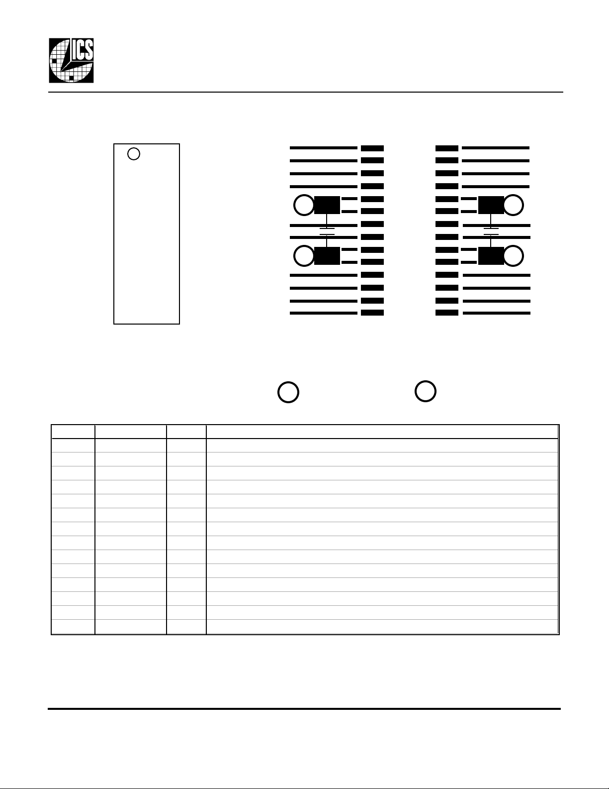
Pin Assignment
INA
1
QA0
2
QA1
3
QA2
4
QA3
QA4
QA5
QA6
QA7
OEA
5
6
7
8
9
10
11
12
13
14
VDD
VDD
GND
GND
28
27
26
25
24
23
22
21
20
19
18
17
16
15
INB
QB0
QB1
QB2
VDD
VDD
QB3
QB4
GND
GND
QB5
QB6
QB7
OEB
Suggested Layout
V
0.1µF
G
For simplicity, terminating resistors are not shown for the
outputs, but should be placed as close to the device as
possible. It is most critical to have the 0.1µF decoupling
capacitors closest.
= connect to VDD
V
= connect to GND
G
V
0.1µF
G
Pin Descriptions
Number Name Type Description
1 INA I Clock input for eight A outputs.
2, 3, 4 QA0, QA1, QA2 O Clock A outputs.
5, 6 VDD P Power supply. Connect to 3.3 V or +5 V. Must be same as pins 23, 24.
7, 8 QA3, QA4 O Clock A outputs.
9, 10 GND P Connect to ground.
11, 12, 13 QA5, QA6, QA7 O Clock A outputs.
14 OEA I Output Enable. Tri-states all A clock outputs when this input is low. Internal pull-up.
15 OEB I Output Enable. Tri-states all B clock outputs when this input is low. Internal pull-up.
16, 17, 18 QB7, QB6, QB5 O Clock B outputs.
19, 20 GND P Connect to ground.
21, 22 QB4, QB3 O Clock B outputs.
23, 24 VDD P Power supply. Connect to +3.3 V or +5 V. Must be same as pins 5, 6.
25, 26, 27 QB2, QB1, QB0 O Clock B outputs.
28 INB I Clock input for eight B outputs.
Type: I = Input, O = output, P = power supply connection
MDS74CB217A 2 Revision 12299 Printed 2/22/00
IntegratedCircuit Systems, Inc. • 525 Race Street • San Jose •CA •95126•(408) 295-9800tel • www.icst.com
Page 3
PRELIMINARY INFORMATION
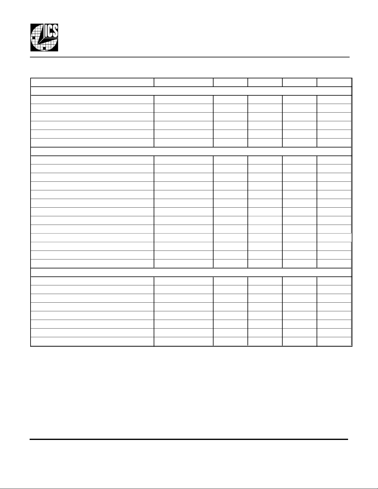
ABSOLUTE MAXIMUM RATINGS (Note 1)
DC CHARACTERISTICS (VDD = 3.3 V unless noted)
AC CHARACTERISTICS (VDD = 3.3 V unless noted)
MK74CB217
Dual 1 to 8 Buffalo™ Clock Driver
Electrical Specifications
Parameter Conditions Minimum Typical Maximum Units
Supply Voltage, VDD Referenced to GND 7 V
Inputs Referenced to GND 0.5 VDD+0.5 V
Clock Outputs Referenced to GND 0.5 VDD+0.5 V
Ambient Operating Temperature 0 70 °C
Soldering Temperature Max of 20 seconds 260 °C
Storage Temperature -65 150 °C
Operating Voltage, VDD 3.0 3.3 5.5 V
Input High Voltage, VIH (INA, INB pins) VDD-1.0 VDD/2 V
Input Low Voltage, VIL (INA, INB pins) VDD/2 1.0 V
Input High Voltage, VIH (OEA, OEB pins) 2.0 V
Input Low Voltage, VIL (OEA, OEB pins) 0.8 V
Output High Voltage, 3.3V and 5V IOH=-12mA VDD-0.4 V
Output High Voltage, 3.3V and 5V IOH=-25mA 2.4 V
Output Low Voltage, 3.3V and 5V IOL=25mA 0.8 V
Operating Supply Current, IDD, at 100 MHz No Load 55 mA
Output Impedance
Short Circuit Current Each output 100 mA
On-Chip Pull-up Resistor OEA, OEB 250 kΩ
Input Capacitance 7 pF
14 Ω
Input Clock Frequency Note 4 0 200 MHz
Propagation Delay with load=15pF 1.4 3 ns
Output Clock Rise Time 0.8 to 2.0V 2 ns
Output Clock Fall Time 2.0 to 0.8V 2 ns
Output Clock Rising Edge Skew At VDD/2. Note 2 100 250 ps
Output Clock A to B Skew At VDD/2. Note 3 100 250 ps
Output Enable Time, OE high to output on 20 ns
Output Disable Time, OE low to tri-state 20 ns
Notes:
1. Stresses beyond those listed under Absolute Maximum Ratings could cause permanent damage to the device. Prolonged exposure
to levels above the operating limits but below the Absolute Maximums may affect device reliability.
2. Between any two A outputs, or any two B outputs, with equal loading.
3. Between any clock A output and any clock B output with INA connected to INB, and equal loading.
4. See discussion and graph of speed versus load.
MDS74CB217A 3 Revision 12299 Printed 2/22/00
IntegratedCircuit Systems, Inc. • 525 Race Street • San Jose •CA •95126•(408) 295-9800tel • www.icst.com
Page 4
PRELIMINARY INFORMATION
MK74CB217
Dual 1 to 8 Buffalo™ Clock Driver
Maximum Speed
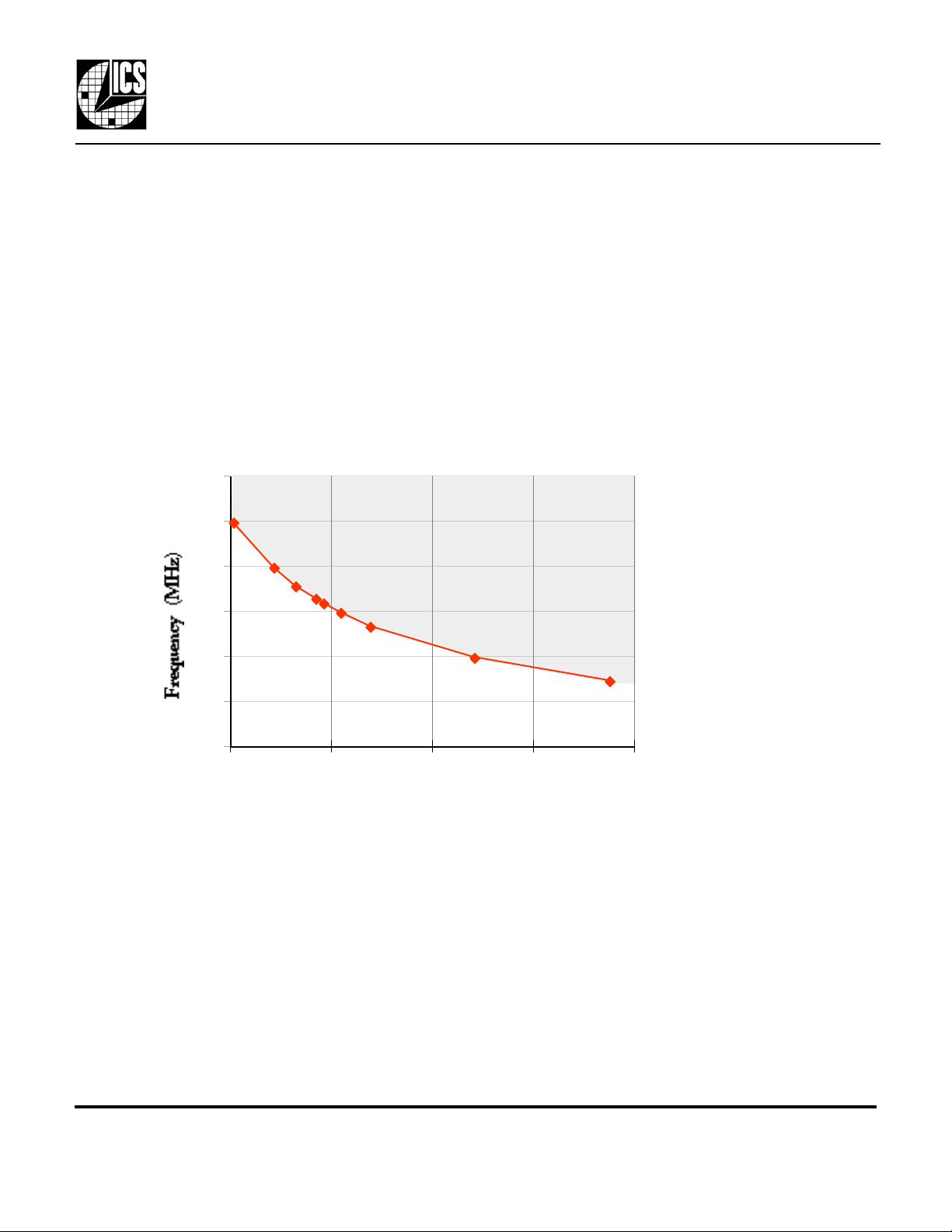
The maximum speed at which the chip can operate is limited by power dissipation in the package. Graph 1
shows the operating frequency plotted against load capacitance per pin for a die temperature of 125°C. This is
at VDD = 3.3 V, 70°C and with 33 Ω series termination resistors. The termination resistors are essential
because they allow a large proportion of the total power to be dissipated outside the package. Reducing or
eliminating the series termination will cause an increase in die temperature. It is not recommended to operate
the chip at die temperatures greater than 125°C. Also note that the load capacitance per pin must include PC
board parasitics such as trace capacitance.
If not all outputs of the chip are used, it is possible to operate the chip faster with larger loads. Consult ICS for
your specific requirement.
300
250
200
150
100
Do not operate in this area.
50
0
806040200
Load Capacitance/per pin (pF)
Graph 1
MK74CB217
Maximum Speed
MDS74CB217A 4 Revision 12299 Printed 2/22/00
IntegratedCircuit Systems, Inc. • 525 Race Street • San Jose •CA •95126•(408) 295-9800tel • www.icst.com
Page 5
PRELIMINARY INFORMATION
Inches
Millimeters
Dual 1 to 8 Buffalo™ Clock Driver
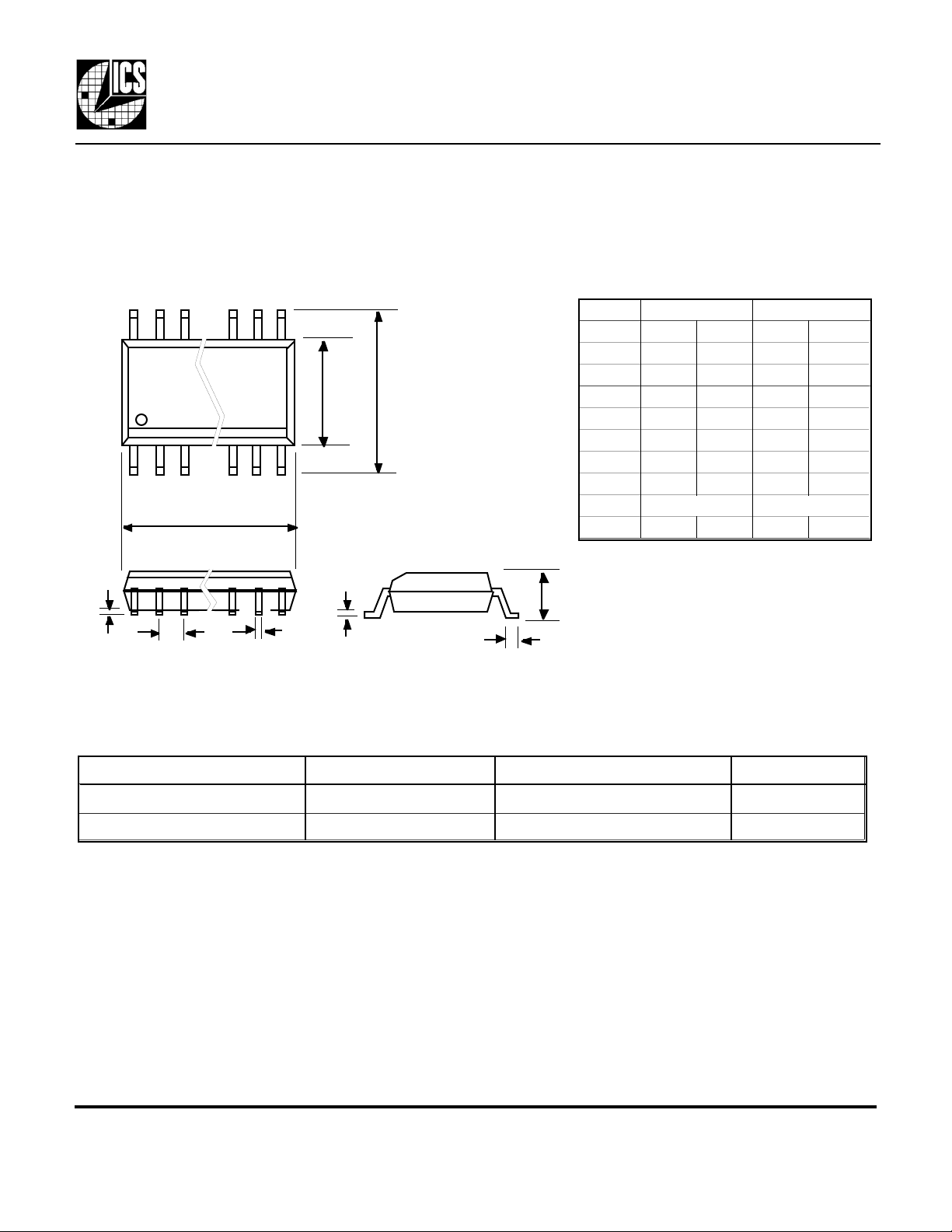
Package Outline and Package Dimensions
(For current dimensional specifications, see JEDEC publication no. 95.)
28 pin SSOP
Symbol Min Max Min Max
A 0.053 0.069 1.35 1.75
E1 E
D
A1 0.004 0.01 0.10 0.25
b 0.008 0.012 0.20 0.30
c 0.007 0.010 0.19 0.25
D 0.386 0.394 9.80 10.01
E1 0.150 0.157 3.81 3.99
E 0.228 0.244 5.79 6.20
e
L 0.016 0.05 0.41 1.27
MK74CB217
A1
A
c
e
b
L
Ordering Information
Part/Order Number Marking Package Temperature
MK74CB217R MK74CB217R 28 pin SSOP 0-70 °C
MK74CB217RTR MK74CB217R Add Tape & Reel 0-70 °C
While the information presented herein has been checked for both accuracy and reliability, ICS Incorporated assumes no responsibility for either its use or for the infringement of
any patents or other rights of third parties, which would result from its use. No other circuits, patents, or licenses are implied. This product is intended for use in normal
commercial applications. Any other applications such as those requiring extended temperature range, high reliability, or other extraordinary environmental requirements are not
recommended without additional processing by ICS. ICS reserves the right to change any circuitry or specifications without notice. ICS does not authorize or warrant any ICS
product for use in life support devices or critical medical instruments.
Buffalo is a trademark of ICS Incorporated
MDS74CB217A 5 Revision 12299 Printed 2/22/00
IntegratedCircuit Systems, Inc. • 525 Race Street • San Jose •CA •95126•(408) 295-9800tel • www.icst.com
 Loading...