

SGS Thomson Microelectronics MC3503, MC3403D, MC3403N, MC3303N, MC3303D Datasheet
...
MC3303
®
MC3403 - MC3503
LOW POWER QUAD BIPOLAR OPERATIONAL AMPLIFIERS
.SHORT-CIRCUIT PROTECTED OUTPUTS
.CLASS AB OUTPUT STAGE FOR MINIMAL
CROSSOVER DISTORTION
.SINGLE SUPPLY OPERATION : + 3 V TO + 36V
.DUAL SUPPLIES : ±1.5V TO ±18V
.LOW INPUT BIAS CU RRE N T : 500nA M A X
.INTERNALLY COMPENSATED
.SIMILAR PERFORMANCE TO POPULAR
UA741
DESCRIPTION
The MC3403 is a low-cos t, quad operation al amplifier with true differential inputs. The device has electrical characteristics similar to the popular UA741.
However the MC3403, has several distinct advantages over standard operational amplifier types in
single supply applications. The quad amplifier can
operate at sup ply v o l tages as low as 3. 0 v olt s or as
high as 36 volts with quiescent currents about one
third of those associated with the UA741 (on a per
amplifier basis ). The c ommon- mode inp ut range i ncludes the negative supply, thereby eliminating the
necessity for external biasing components in many
applications .
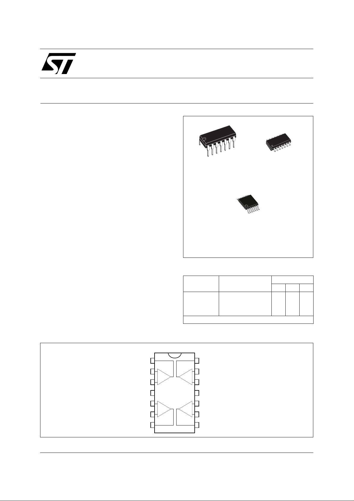
ORDER CODES
Part
Number
MC3303 –40
MC3403 0
MC3503 –55
Example : MC3403N
N
DIP14
(Plast ic Pac kag e)
(Thin Shrink Small Outline Package)
Temperature
o
(Plastic Micropackage)
P
TSSOP14
Range
o
C, +105oC •••
C, +70oC •••
o
C, +125oC •••
D
SO14
Package
NDP
PIN CONNECTIONS (top view)
Output 1
Inverting Input 1
Non-inverting Input 1
Non-inverting Input 2
Inverting Input 2
Output 2
August 1998
V
CC
1
2
-
+
3
+
4
5
+
-
6
7
14
Output 4
13
-
+
+
-
Inverting Input 4
12
Non-inverting Input 4
11
10
-
V
CC
Non-inverting Input 3
9
Inverting Input 3
8
Output 3
1/11
MC3303 - MC3 403 - MC35 03
SCHEMATIC DIAGRAM (each ampli fier)
Non-inverting
input
Inverting
input
(1 stage)
Q23
Q22 Q24
Q21
Q2
Q3
Output
Q19
Q20
C1
8pF
Q25
Q6
Q5
Q4
12k
Q7
Q14
R1
Ω
Q18
Q1
R6
Ω
0.7k
Q9
Q8
31k
37 k
Q17
Q16
R4
Ω
Q15
Q13
R2
Ω
Q12
Q11
Q10
Q27
Q28
R3
Ω
25
Q30
R5
8.2k
Ω
Q29
V
CC
(Ground)
V
CC
SINGL E SUP PLY
+3V to +30V
V
CC
V
CC
DUAL SUPPLIES
V
CC
1.5V to 18V
1.5V to 18V
V
CC
ABSOLUTE MAXIMUM RATINGS
Symbol Parameter MC3503 MC3403 MC3303 Unit
V
P
T
T
Notes : 1. For supply voltages less than ±15V , the abs ol ute maxi mum inpu t volt age is equal to the supply volt ag e.
Supply Voltage ±18 or 36 ±18 or 36 ±18 or 36 V
CC
Differential Input Voltage ±36 ±36 ±36 V
V
id
Input Voltage (note 1) ±18 ±18 ±18 V
V
i
– Output Short-circuit Duration (note 2) Infinite –
Power Dissipation 500 500 500 mW
tot
Operating Free-air Temperature Range –55 to +125 0 to +70 –40 to +105
oper
Storage Temperature Range –65 to +150 –65 to +150 –65 to +150
stg
2. Any of the amplifier outputs can be shorted to ground indefin itel y ; however more than one shou ld not be simultaneous ly short ed
as the maximum junc tio n te mpe rat ure wil l be excee d ed.
o
C
o
C
2/11
ELECTRICAL CHARACTERISTICS
V
= ±15V, T
CC
Symbol Parameter
V
IO
I
IO
I
ib
A
vd
SVR Supply Voltage Rejection Ratio (R
I
CC
V
icm
CMR Common Mode Rejection Ratio (R
I
OS
± V
opp
SR Slew Rate (V
, t
t
r
f
K
OV
Z
I
Z
O
B
om
B Unity Gain Bandwidth (V
GBP Gain Bandwidth Product (V
THD Total Harmonic Distortion (f = 1kHz, A
e
n
= +25oC, (unless otherwise specified)
amb
Input Offset Voltage (RS ≤ 10kΩ)
T
= 25oC
amb
T
≤ T
amb
≤ T
max.
min.
Input Offset Current
= 25oC
T
amb
T
≤ T
amb
≤ T
max.
min.
Input Bias Current
T
= 25oC
amb
≤ T
T
min.
amb
≤ T
max.
Large Signal Voltage Gain (VO = ±10V, RL = 2kΩ)
T
= 25oC
amb
T
≤ T
amb
= 25oC
≤ T
amb
≤ T
≤ T
max.
max.
min.
T
amb
T
min.
Supply Current, all Amp, no Load
T
= 25oC
amb
≤ T
T
min.
amb
≤ T
max.
Input Common Mode Voltage Range
T
= 25oC
amb
≤ T
T
min.
T
amb
T
min.
amb
= 25oC
≤ T
amb
≤ T
≤ T
max.
max.
Output Short-circuit Current 10 30 45 mA
Output Voltage Swing
= 25oCR
T
amb
T
≤ T
min.
T
= 25oC, unity gain) 0.35 0.5
amb
≤ T
amb
max.
= ±10V RL = 2kΩ, CL = 100pF,
I
Rise Time and Fall T ime (VO = ± 20mV, RL = 2kΩ, CL = 100pF
T
= 25oC, unity gain) 0.18
amb
Overshoot (VI = ± 20mV, RL = 2kΩ, CL = 100pF,
= 25oC, unity gain) 10
T
amb
Input Impedance 0.3 1 MΩ
Output Impedance 75 Ω
Power Bandwidth (RL = 2kΩ, CL = 100pF, Av = 1, T
VO = 2Vpp, THD ≤ 5%) 9
= 10mV, RL = 2kΩ, CL = 100pF,
T
= 25oC, unity gain) 1
amb
f = 100kHz, T
= 25oC) 0.7 1
amb
VO = 2Vpp, CL = 100pF, T
O
= 10mV, RL = 2kΩ, CL = 100pF,
O
= 25oC) 0.02
amb
Equivalent Input Noise Voltage (f = 1kHz, Rs = 100Ω)43
≤ 10kΩ)
S
≤ 10kΩ)
S
= 20dB, RL = 2kΩ,
v
MC3303 - MC3 403 - MC35 03
Min. Typ. Max.
50
25
77
77
MC3503
MC3503
– 15
– 15
70
70
= 10kΩ
L
RL = 2kΩ
RL = 2kΩ
= 10kΩ
R
L
= 25oC,
amb
12
10
10
12
MC3303 - MC3403
MC3503
15
250
200
40 500
800
200
90
2.8 7
+ 13
+ 13
90
13.5
13
Unit
mV
6
nA
nA
V/mV
dB
mA
4
8
5
V
dB
V
V/µs
µs
%
kHz
MHz
MHz
%
nV
√Hz
3/11
MC3303 - MC3 403 - MC35 03
ELECTRICAL CHARACTERISTICS (continued)
Symbol Parameter
∅m Phase Margin 60 Degrees
DV
DI
IO
V
O1/V02
ELECTRICAL CHARACTERISTICS
+
V
= 5V, V
CC
Input Offset Voltage Drift
IO
T
≤ T
amb
≤ T
max.
min.
Input Offset Current Drift
T
min
. ≤ T
≤ 25oC50
amb
Channel Separation 120 dB
–
= Ground, T
CC
= 25oC (unless otherwise specified)
amb
Symbol Parameter
V
IO
I
IO
I
ib
A
vd
SVR Supply Voltage Rejection Ratio (R
I
CC
V
opp
Input Offset Voltage (RS ≤ 10kΩ)
T
= 25 °C
amb
T
≤ T
amb
≤ T
max
min
Input Offset Current
T
= 25oC
amb
≤ T
T
min.
amb
≤ T
max.
Input Bias Current
T
= 25oC
amb
≤ T
T
min.
amb
≤ T
max.
Large Signal Voltage Gain (VO = 1.4 to 2.4V, RL = 2kΩ)
T
= 25oC
amb
T
≤ T
amb
= 25oC
≤ T
amb
≤ T
≤ T
max.
max.
≤ 10kΩ)
S
min.
T
amb
T
min.
Supply Current (All Amp)
MC3503
Output Voltage Range (RL = 10kΩ)
V
= +5V
CC
+5 < V
≤ +30V
CC
MC3303 - MC3403 - MC3503
Min. Typ. Max.
10
MC3303 - MC3403 - MC3503
Min. Typ. Max.
15
6
250
200
40 500
800
10
200
5
77
90
77
2.5 7
4
3.3
+
V
-2V
CC
3.5
+
V
-1.7V
CC
Unit
µV/oC
pA/oC
Unit
mV
nA
nA
V/mV
dB
mA
V
4/11
 Loading...