

SGS Thomson Microelectronics MC33079, MC33079D, MC33079N Datasheet
LOW NOISE QUAD OPERATIONAL AMPLIFIERS
.
LOW VOLTAGE NOISE: 4.5nV/√√Hz
.
HIGHGAIN BANDWIDTHPRODUCT: 15MHz
.
HIGHSLEW RATE : 7V/µµs
.
LOW DISTORTION : 0.002%
.
LARGE OUTPUT VOLTAGE SWING :
+14.3V/-14.6V
.
EXCELLENTFREQUENCY STABILITY
.
ESD INTERNALPROTECTION
.
MACROMODEL INCLUDED IN THIS
SPECIFICATION
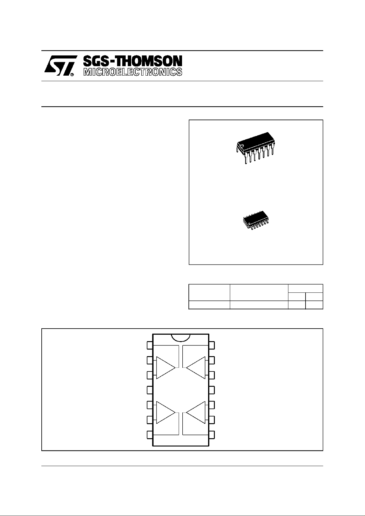
MC33079
N
DIP14
(Plastic Package)
DESCRIPTION
The MC33079 is a monolithic quad operational
amplifier particularly well suited for audio applications. It offerslow voltage noise (4.5nV/√Hz ) and
high frequencyperformances (15MHzGain Bandwidth product, 7V/µsslew rate).
In addition the MC33079has a verylow distortion
(0.002%)and excellentphase/gainmargins.
The output stage allows a large output voltage
swing andsymmetrical source and sink currents.
PIN CONNECTIONS (top view)
CC
1
2
3
+
4
5
-
+
+
Output 1
Inverting Input 1
Non-inverting Input 1
V
Non-inverting Input 2
D
SO14
(Plastic Micropackage)
ORDER CODES
Part Number Temperature Range
o
MC33079 -40, +105
14
Output 4
13
-
+
+
Inverting Input 4
12
Non-inverting Input 4
-
V
11
CC
10
Non-inverting Input 3
C ••
Package
ND
November 1997
Inverting Input 2
Output 2
6
7
-
-
9
Inverting Input 3
8
Output 3
1/9
MC33079
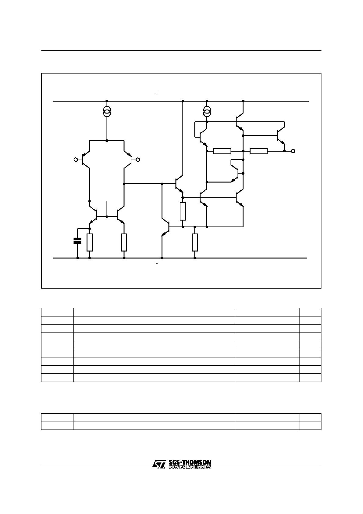
SCHEMATIC DIAGRAM (1/4MC33079)
V
CC
Inverting
Input
Non-inve rting
Input
V
CC
ABSOLUTEMAXIMUMRATINGS
Symbol Parameter Value Unit
Output
V
CC
V
id
V
T
oper
T
T
stg
P
tot
Notes : 1. Either or both input voltages mustnotexceed the magnitude of V
Supply Voltage ±18 or +36 V
Differential Input Voltage - (note 1) ±30 V
Input Voltage- (note 1) ±15 V
i
Output Short-Circuit Duration - (note 2) Infinite
Operating Free-air Temperature Range -40 to +105
Maximum Junction Temperature +150
j
Storage Temperature -65 to +150
Maximum Power Dissipation - (note 2) 500 mW
+
-
or V
CC
2. Power dissipation must be considered to ensure maximum junction temperature (Tj) is not exceeded
CC
o
C
o
C
o
C
OPERATINGCONDITIONS
Symbol Parameter Value Unit
Supply Voltage ±2.5 to ±15 V
2/9
V
CC
MC33079
ELECTRICAL CHARACTERISTICS
+
= +15V,V
V
CC
Symbol Parameter Min. Typ. Max. Unit
V
io
DV
io
I
io
I
ib
V
icm
A
vd
±V
opp
CMR Common Mode Rejection Ratio (V
SVR SupplyVoltage RejectionRatio
I
o
I
CC
SR Slew Rate
GBP Gain Bandwidth Product (f = 100kHz, R
B Unity Gain Bandwidth (Open loop) 9 MHz
A
m
∅m Phase Margin (R
e
n
i
n
THD Total Harmonic Distortion
V
O1/VO2
FPB Full Power Bandwidth (V
Z
o
R
i
C
i
-
= -15V,T
CC
Input Offset Voltage (Vo= 0V, Vic= 0V)
≤ T
T
min.
amb
=25oC (unlessotherwisespecified)
amb
≤ T
max.
2.5
3.5
Input Offset Voltage Drift
= 0V, Vo= 0V, T
V
ic
min.
≤ T
amb
≤ T
max.
2
Input Offset Current (Vic=0V,VO= 0V)
T
T
amb
min.
= +25oC
≤ T
amb
≤ T
max.
10 150
175
Input Bias Current (Vic= 0V, VO= 0V)
T
T
amb
min.
= +25oC
≤ T
amb
≤ T
max.
250 750
800
Common Mode Input Voltage Range (∆VIO= 5mV, VO= 0V) ±13 ±14 V
Large Signal Voltage Gain (RL=2kΩ,VO=±10V)
T
T
amb
min.
= +25oC
≤ T
amb
≤ T
max.
90
85
100
Output Voltage Swing (Vid= ±1V)
= 600Ω
R
L
= 600Ω
R
L
R
= 2.0kΩ
L
= 2.0kΩ
R
L
R
= 10kΩ
L
= 10kΩ
R
L
= ±13V) 80 100 dB
ic
+
-
/V
V
CC
= +15V / -15V to +5V / -5V 80 105
CC
13.2
13.5
12.2
-12.7
14
-14.2
14.3
-14.6
-13.2
-14
Output Short Circuit Current (Vid= ±1V, Output to Ground)
Source
Sink
15
20
29
37
Supply current (VO= 0V, All Amplifiers)
= +25oC
T
amb
≤ T
T
min.
= -10Vto +10V, RL=2kΩ,CL= 100pF, AV=+1 5 7
V
i
Gain Margin(RL=2kΩ)C
≤ T
amb
max.
=2kΩ,CL= 100pF) 10 15 MHz
L
L
C
L
=2kΩ)C
L
L
C
L
= 0pF
= 100pF
= 0pF
= 100pF
810
12
-11
-6
55
30
Equivalent Input Noise Voltage (RS= 100Ω, f = 1kHz) 4.5
Equivalent Input Noise current (f = 1kHz) 0.5
=2kΩ, f = 20Hz to 20kHz, VO=3V
R
L
= +1 0.002
rms,AV
Channel Separation (f = 20Hz to 20kHz) 120 dB
= 27Vpp,RL=2kΩ, THD ≤ 1%) 120 kHz
O
Output Impedance (VO= 0V, f = 9MHz) 37 Ω
Input Resistance (Vic= 0V) 175 kΩ
Input Capacitance (Vic= 0V) 12 pF
mV
o
µV/
C
nA
nA
dB
V
dB
mA
mA
V/µs
dB
Degrees
nV
Hz
√
pA
Hz
√
%
3/9
 Loading...