

SGS Thomson Microelectronics M95256-WMW1T, M95256-WMW1, M95256-WBN6, M95256-WBN5, M95256-VMW6 Datasheet
...
1/21
PRELIMINARY DATA
March 2000
This is preliminary information on a new product now in development or undergoing evaluation. Details are subject to change without notice.
M95256
M95128
256/128 Kbit Serial SPI Bus EEPROM
With High Speed Clock
■ SPI Bus Compatible Serial Interface
■ Supports Positive Clock SPI Modes
■ 5 MHz Clock Rate (maximum)
■ Single Supply Voltage:
– 4.5V to 5.5V for M95xxx
– 2.7V to 3.6V for M95xxx-V
– 2.5V to 5.5V for M95xxx-W
– 1.8V to 3.6V for M95xxx-R
■ Status Register
■ Hardware and Software Protection of the Status
Register
■ BYTE and PAGE WRITE (up to 64 Bytes)
■ Self-Tim ed P ro gr a m ming Cycle
■ Resizeable Read-Only EEPROM Area
■ Enhanced ESD Protection
■ 100,000 Erase/Write Cycles (minimum)
■ 40 Year Data Retention (minimum)
DESCRIPTION
These SPI-compatible electrically erasable
programmable memory (EEPROM) devices are
organized as 32K x 8 bits (M9525 6) and 16K x 8
bits (M95128), and operate down to 2.7 V (for the
Figure 1. Logic Diagram
AI01789C
S
V
CC
M95xxx
HOLD
V
SS
W
Q
C
D
Table 1. Signal Names
C Serial Clock
D Serial Data Input
Q Serial Data Output
S
Chip Select
W
Write Protect
HOLD
Hold
V
CC
Supply Voltage
V
SS
Ground
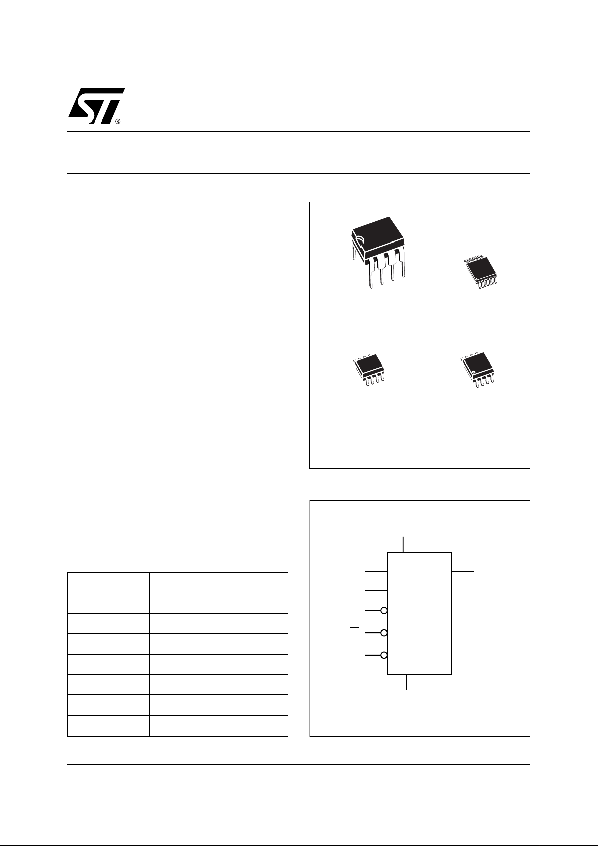
PSDIP8 (BN)
0.25 mm frame
SO8 (MN)
150 mil width
TSSOP14 (DL)
169 mil width
8
1
8
1
14
1
SO8 (MW)
200 mil width
8
1
M95256, M95128
2/21
-V version), 2.5 V (for the -W version), and down
to 1.8 V (for the -R version of each device).
The M95256 and M 95128 are available in Plastic
Dual-in-Line, Plastic Small Outline and Thin Shrink
Small Outline packages.
Each memory device is accessed by a simple
serial interface that is SPI bus compatible. The bus
signals are C, D and Q, as shown in Table 1 and
Figure 3.
The device is selected when t he chip select input
(S
) is held low. Communications with the chip can
be interrupted using the hold input (HOLD
).
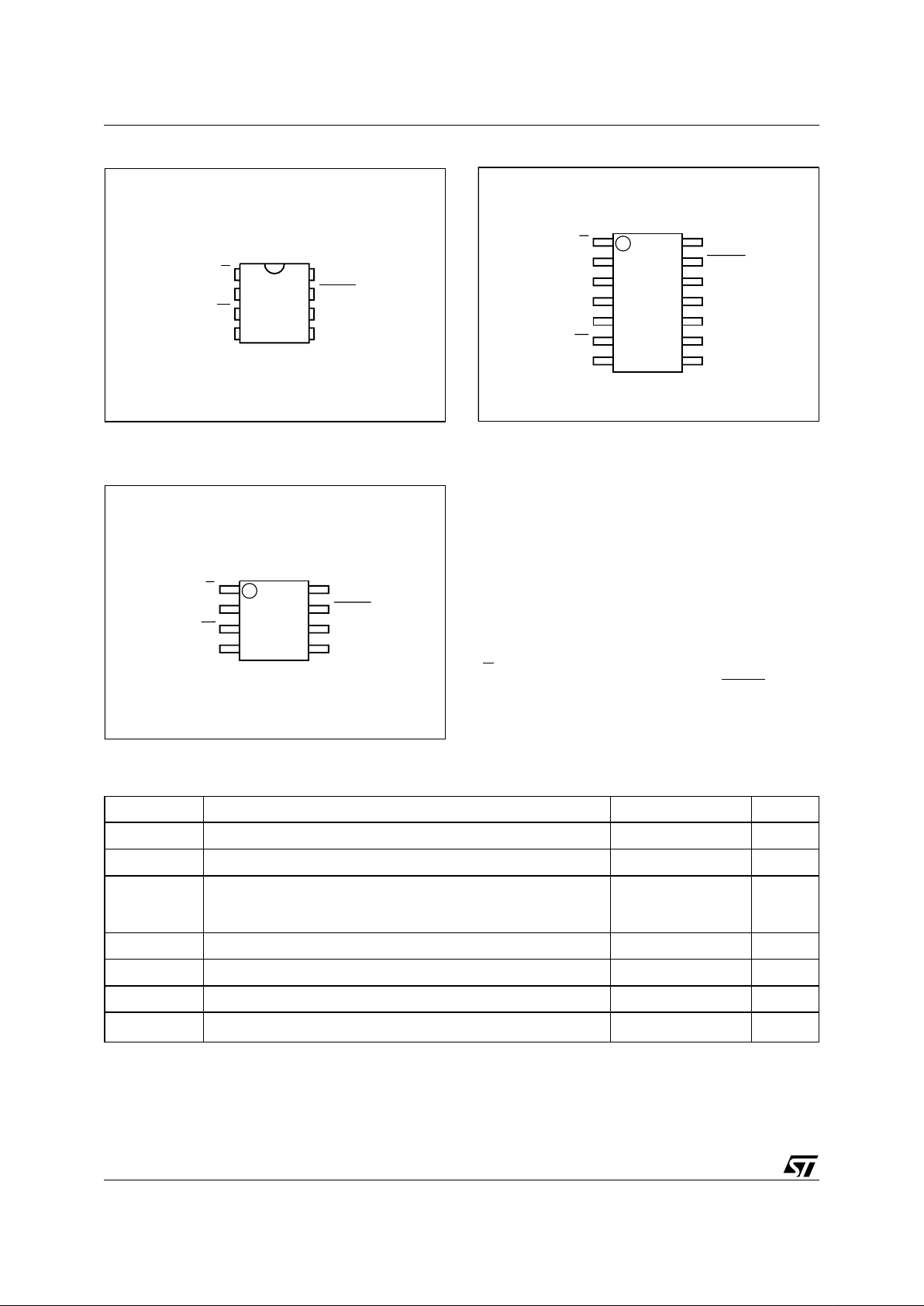
Figure 2A. DIP Connections
Figure 2B. SO C on ne ct i on s
DV
SS
C
HOLDQ
SV
CC
W
AI01790C
M95xxx
1
2
3
4
8
7
6
5
1
AI01791C
2
3
4
8
7
6
5
DV
SS
C
HOLDQ
SV
CC
W
M95xxx
Figure 2C. TSSOP Connections
Note: 1. NC = Not Connected
1
AI02346
2
3
4
14
9
10
8
DV
SS
WC
S
HOLD
M95128
NC
Q
NC
NC NC
NC
NC
5
6
7
12
13
11
V
CC
Table 2. Absolute Maximum Ratings
1
Note: 1. Except for the rating “Operating Tempera ture Range”, stres ses above th ose listed i n the Tabl e “Absolute Maxim um Ratings” may
cause permanent damage to the device. These are stress ratings only, and operation of the device at these or any other conditions
above those indicated in the Operating sections of this specification is not implied. Exposure to Absolute Maximum Rating
conditions for extended periods may affect device reliability. Refer also to the ST SURE Program and other relevant quality
document s.
2. M IL-STD-883C, 3015.7 (100 pF, 1500 Ω)
Symbol Parameter Value Unit
T
A
Ambient Operating Temperature -40 to 125 °C
T
STG
Storage Temperature -65 to 150 °C
T
LEAD
Lead Temperature during Soldering
PSDIP8: 10 sec
SO8: 40 sec
TSSOP14: t.b.c.
260
215
t.b.c.
°C
V
O
Output Voltage Range
-0.3 to V
CC
+0.6
V
V
I
Input Voltage Range -0.3 to 6.5 V
V
CC
Supply Voltage Range -0.3 to 6.5 V
V
ESD
Electrostatic Discharge Voltage (Human Body model)
2
4000 V
3/21
M95256, M95128
SIGNAL DESCRIPTION
Seria l O utput ( Q )
The output pin is used to transfer data serially out
of the Memory. Data is shifted out on the falling
edge of the serial clock.
Serial Inpu t ( D )
The input pin is used to transfer data serially into
the device. Instructions, addresses, and the data
to be written, are each received this way . Input is
latched on the rising edge of the serial clock.
Serial Clock (C)
The serial clock provides the timing for the serial
interface (as shown in Figure 4). Instructions,
addresses, or data are latched, from the input pin,
on the rising edge of the clock input. The output
data on the Q pin chang es state after the falling
edge of the clock input.
Chip Select (S
)
When S
is high, the memory device is deselected,
and the Q output pin is held in its high impe dance
state. Unless an internal write operation is
underway, the memory device is placed in its
stand-by power mode.
After power-on, a high-to-low transition on S
is
required prior to the start of any operation.
Write Protect (W
)
The protection features of t he m em ory device are
summarized in Table 3.
The hardware write protection, controlled by the W
pin, restricts write access to the Status Register
(though not to the WIP and WEL bits, which are
set or reset by the device internal logic).
Bit 7 of the status register (as shown in Table 5) is
the Status Register Write Disable bit (SRWD).
When this is set to 0 (its initial delivery state) it is
possible to write to the status register if the WEL
bit (Write Enable Latch) has been set by the
WREN instruction (irrespective of the l evel being
applied to the W
input).
When bit 7 (SRWD) of the st atus register is set to
1, the ability to write to the status register depends
on the logic level being presented at pin W
:
–If W
pin is high, it is possible to write to the
status register, after having set the WEL bit
using the WREN instruction (Write Enable
Latch).
–If W
pin is low, any attempt to modify the status
register is ignored by the device, even if the
WEL bit has been set. As a consequence, all the
data bytes in the EE PROM area, protected by
the BPn bits of the status register, are also
hardware protected against data corruption,
and appear as a Read Only EEPROM area for
the microcontroller. This mode is called the
Hardware Protected Mode (HPM).
It is possible to enter the Hardware Protected
Mode (HPM) either by s etting the SRWD bi t after
pulling low the W
pin, or by pulling low the W pin
after setting the SRWD bit.
The only way to abort the Hardware Protected
Mode, once entered, is to pull high the W
pin.
If W
pin is permanently t ied to the hi gh level, the
Hardware Protected Mode is never activated, and
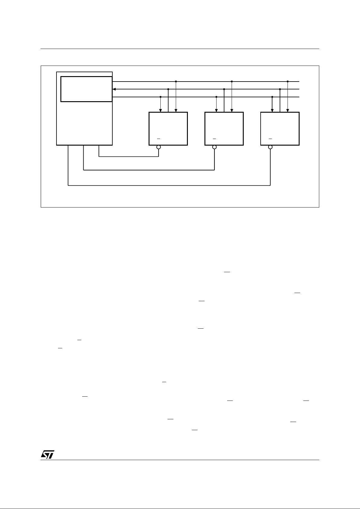
Figure 3. Microcontroller and Memor y Devices on the SPI Bus
AI01958C
Master
(ST6, ST7, ST9,
ST10, Others)
M95xxx
SDO
SDI
SCK
CQD
S
M95xxx
CQD
S
M95xxx
CQD
S
CS3 CS2 CS1
SPI Interface with
(CPOL, CPHA) =
('0', '0') or ('1', '1')
M95256, M95128
4/21
the memory device only allows the user to protect
a part of the memory, usi ng the BPn bits of the
status register, in the Software Protected Mode
(SPM).
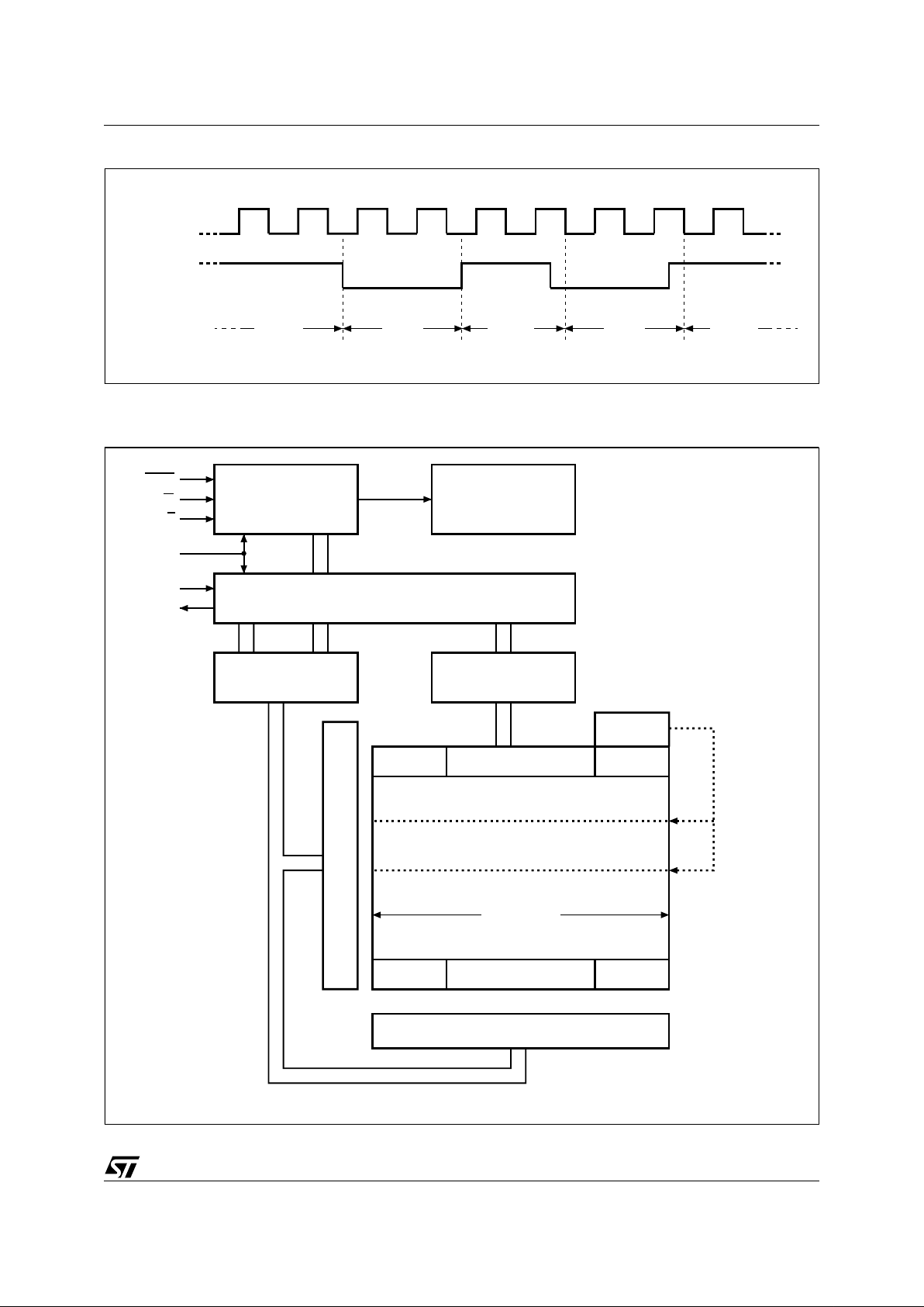
Hold (HOLD
)
The HOLD
pin is used to pause the serial
communications between the SPI memory and
controller, without losing bits that have already
been decoded in the serial sequence. For a hold
condition to occur, the memory device must
already have been selected (S
= 0). The hold
condition starts when the HOLD
pin is held low
while the clock pin (C) is also low (as shown in
Figure 5).
During the hold condition, the Q output pin i s held
in its high impedance sta te, and the level s on the
input pins (D and C) are ignored by the memory
device.
It is possible to deselect the device whe n it is still
in the hold state, thereby resetting whatever
transfer had been in progress. The memory
remains in the hold state as long as the HOLD
pin
is low. To restart communication with the device, it
is necessary both to remove the hold condition (by
takin g HO LD
high) and to select the memory (by
taking S
low).
OPERATIONS
All instructions, addresses and data are shifted
serially in and out of the chip. The most significant
bit is presented first, with the data input (D)
sampled on the first rising edge of the clock (C)
after the chip select (S
) goes low.
Every instruction starts with a single-byte code, as
summarized in Table 4. This code is entered via
the data input (D), and latched on the rising edge
of the clock input (C). To enter an instruction code,
the product must have been previously selected (S
held low). If an invalid i nstruction is sent (one not
contained in Table 4), the chip automatically
deselects itself.
Write Enable (WREN) and Write Disable (WRDI)
The write enable latch, inside the memory device,
must be set prior to each WRITE and WRSR
operation. The WREN instruction (write enable)
sets this latch, and the WRDI instruction (write
disable) resets it.
The latch becomes reset by any of the following
events:
– Power on
– WRDI instruction completion
– WRSR in s t ru ctio n completio n
– WRITE instruction completion.
Table 3. Write Protection Control on the M95256 and M95128
W
SRWD
Bit
Mode Status Register
Data Bytes
Protected Area Unprotected Area
0 or 1 0 Software
Protected
(SPM)
Writeable (if the WREN
instruction has set the
WEL bit)
Software write protected
by the BPn of the status
register
Writeable (if the WREN
instruction has set the
WEL bit)
11
01
Hardware
Protected
(HPM)
Hardware write protected
Hardware write protected
by the BPn bits of the
status register
Writeable (if the WREN
instruction has set the
WEL bit)
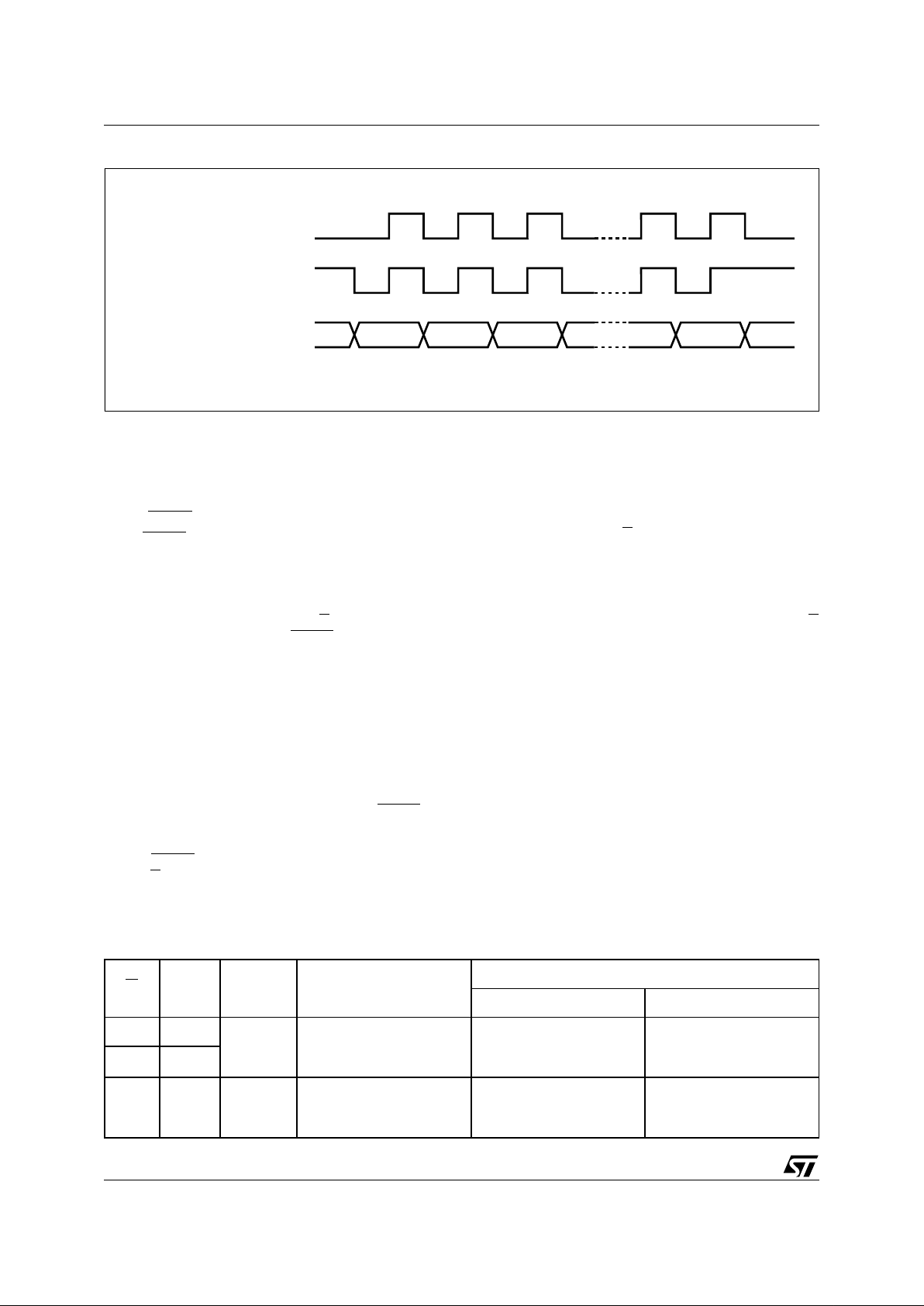
Figure 4. Dat a and Clock Timi ng
AI01438
C
C
MSB LSB
CPHA
D or Q
0
1
CPOL
0
1
5/21
M95256, M95128
Figure 5. Hold Condition Activation
Figure 6. Block Diagram
Note: 1. The cell
An
represents the byte at the highest address in the memory
AI02029B
HOLD PIN
CLOCK
ACTIVE
MEMORY
STATUS
HOLD ACTIVE HOLD ACTIVE
AI02030B
HOLD
S
W
Control Logic
High Voltage
Generator
I/O Shift Register
Address Register
and Counter
Data
Register
64 Bytes
X Decoder
Y Decoder
Size of the
Read only
area of the
EEPROM
C
D
Q
Status
Register
AnAn - 63
003Fh0000h
M95256, M95128
6/21
As soon as the WREN or WRDI instruction is
received, the memory device first executes the
instruction, then enters a wait mode until the
device is deselected.
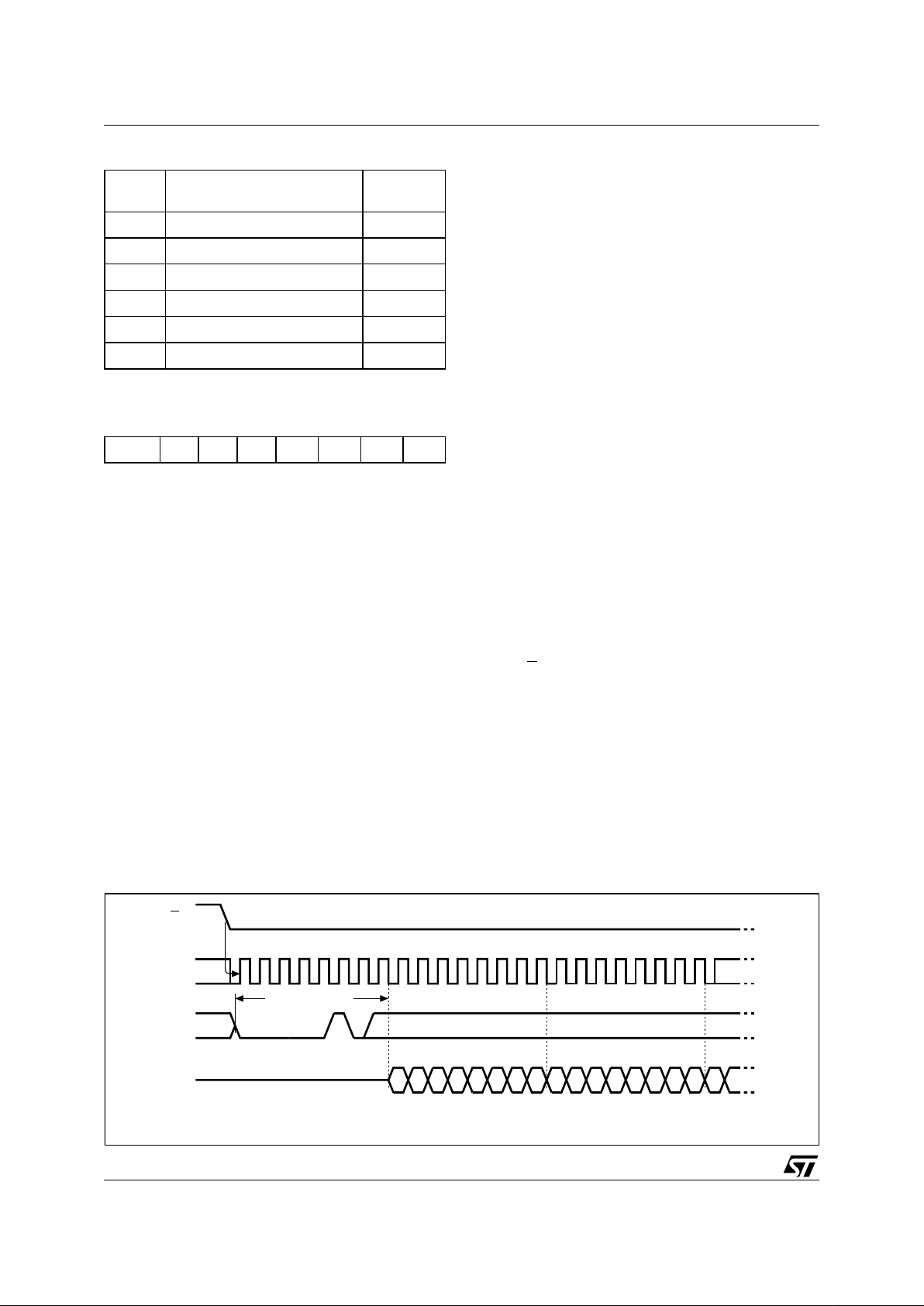
Read Status Register (RDSR)
The RDSR instruction allows the status register to
be read, and can be sent at any time, even during
a Write operation. Indeed, when a Write is in
progress, it is recommended th at the value of t he
Write-In-Progress (WIP) bit be checked. The value
in the WIP bit (whose position in the status register
is shown in Table 5) can be continuously p olled,
before sending a new WRITE instruction, using
the timing shown in Figure 7. The Write-InProcess (WIP) bit is read-only, and indicates
whether the memory is busy with a Write
operation. A ’1’ indicates that a write is in progress,
and a ’0’ that no write is in progress.
The Write Enable Latch (WEL) bit indicates the
status of the write enable latch. It, too, is read-only.
Its value can only be changed by one of the events
listed in the previous paragraph, or as a result of
executing WREN or WRDI instruction. It cannot be
changed using a WRSR instruction. A ’1’ indicates
that the latch is set (the forthcoming Write
instruction will be executed), and a ’0’ that it is
reset (and any forthcoming Write instructions will
be ignored).
The Block Protect (BP0 and BP1) bits indicate the
amount of the memory that is to be writeprotected. These two bits are non-volatile. They
are set using a WRSR instruction.
During a Write operation (whether it be to the
memory area or to the status register), all bits of
the status register remain valid, and can be read
using the RDSR instruction. However, during a
Write operation, the values of the no n-vo latile bits
(SRWD, BP0, BP1) be come frozen at a constant
value. The updated value of these bi ts becomes
available when a new RDSR instruction is
executed, after completio n of the write cycle. On
the other hand, the two read-only bits (WEL, WIP)
are dynamically updated during internal write
cycles. U sing t his fac ility, it is possib le to p oll the
WIP bit to detect the end of the internal write cycle.
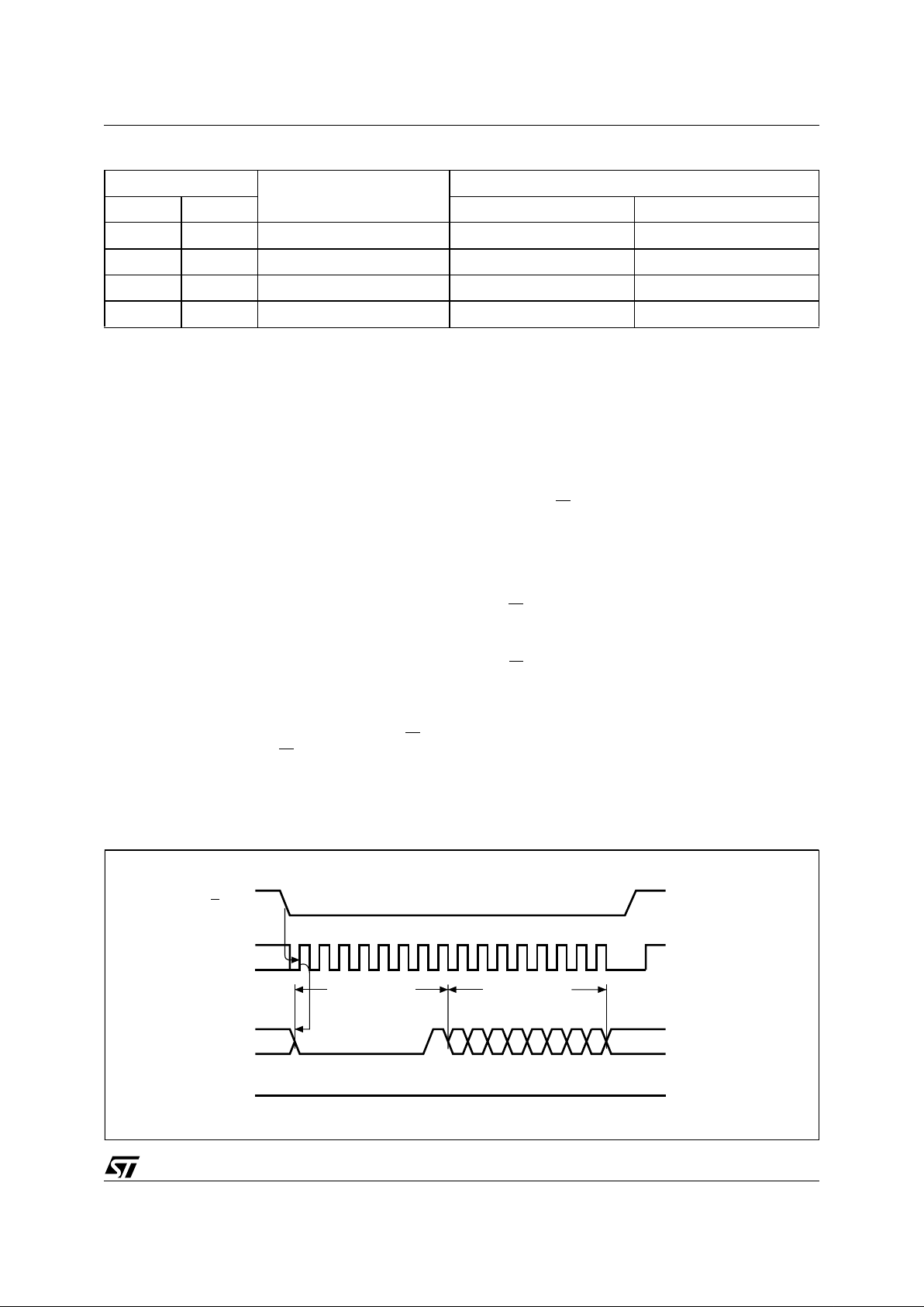
Write Status Register (WRSR)
The format of the WRSR instruction is shown in
Figure 8. After the instruction and the eigh t bits of
the status register have been latched-in, the
internal Write cycle is triggered by the rising edge
of the S
line. This must occur before the rising
edge of the 17
th
clock pulse (as indicated in Figure
14), otherwise the internal write sequence is not
performed.
The WRSR instruction is used for the following:
■ to select the size of memory area that is to be
write-protected
■ to select between SPM (Software Protected
Mode) and HPM (Hardware Protected Mode).
Figure 7. RDSR: Read Status Register Sequence
C
D
S
21 3456789101112131415
INSTRUCTION
0
AI02031
Q
7 6543210
STATUS REG. OUT
HIGH IMPEDANCE
MSB
7 6543210
STATUS REG. OUT
MSB MSB
7
Table 4. Instruction Set
Table 5. Status Register Format
Note: 1. SRWD, BP0 and BP1 are Read and wri te bits.
2. WEL and WIP are Read only bits.
Instruc
tion
Description
Instruction
Format
WREN Set Write Enable Latch 0000 0110
WRDI Reset Write Enable Latch 0000 0100
RDSR Read Status Register 0000 0101
WRSR Write Status Register 0000 0001
READ Read Data from Memory Array 0000 0011
WRITE Write Data to Memory Array 0000 0010
b7 b0
SRWD X X X BP1 BP0 WEL WIP
7/21
M95256, M95128
The size of the write-protection area applies
equally in SPM and HPM. The BP1 and BP0 bits
of the status register have the appropriate value
(see Table 6) written into them after the contents
of the protected area of the EEPROM have been
written.
The initial delivery state of the BP1 and BP0 bits is
00, indicating a write-protection size of 0.
Software Protected Mode (SPM)
The act of writing a non-zero value to the BP1 and
BP0 bits causes the Software Protected Mode
(SPM) to be started. All attempts to write a byte or
page in the protected area are ignored, even if the
Write Enable Latch is set. However, writing is still
allowed in the unprotected area of the memory
array and to the SRWD, BP 1 and BP 0 bits of the
status register, provided that the WEL bit is first
set.
Hardware Prot ected Mode (H P M)
The Hardware Protected Mode (HPM) offers a
higher level of protection, and can be selected by
setting the SRWD bit after pulling down the W
pin
or by pulling down the W
pin after setting the
SRWD bit. The SRWD is set by the WSR
instruction, provided that the WEL bit is first set.
The setting of the SRWD bit can be made
independently of, or at the same time as, writing a
new value to the BP1 and BP0 bits.
Once the device is in the Hardware Protected
Mode, the data bytes in the protected area of the
memory array,
and
the content of the status
register, are write-protected. The only way to reenable writing new v alue s t o t he s tatus register is
to pull the W
pin high. This cause the device to
leave the Hardware Protected Mode, and to revert
to being in the Software Protected Mode. (The
value in the BP1 and BP0 bits will not have been
changed).
Further details of the operation of the Write Protect
pin (W
) is given earlier, on page 3.
Typical Use of HPM and SPM
The W
pin can be dynamically driven by an output
port of a microcontroller. It is also possible,
though, to connect it permanently to V
SS
(by a
solder connection, or through a pull-down
resistor). The manufacturer of such a printed
circuit board can take the memory device, still in its
initial delivery state, and can solder it directly on to
the board. After power on, the microcontroller can
be instructed to write the protected data into the
Table 6. Write Protected Block Size
Status Register Bits
Protected Block
Array Addresses Protected
BP1 BP0 M95256 M95128
0 0 none none none
0 1 Upper quarter 6000h - 7FFFh 3000h - 3FFFh
1 0 Upper half 4000h - 7FFFh 2000h - 3FFFh
1 1 Whole memory 0000h - 7FFFh 0000h - 3FFFh
Figure 8. WRSR: Write Status Register Sequence
C
D
AI02282
S
Q
21 3456789101112131415
HIGH IMPEDANCE
INSTRUCTION STATUS REG.
0
765432 0
1
MSB
 Loading...